
Heat Dissipation Challenges and Solutions in PCB Circuit Board Design
Circuit boards are more than just that green board in a phone
Recently, while researching the development trends of communication equipment, I discovered an interesting phenomenon—those seemingly insignificant printed circuit boards are actually quietly changing our lifestyles. I remember last year when I disassembled an old router and saw the densely packed circuit boards inside, I suddenly realized that this small board carries the entire digital world.
Now, many people, when discussing 5G or future 6G technologies, always focus on chip performance but ignore the bridges connecting these chips. In fact, as IoT devices become increasingly prevalent, every smart device around us needs a reliable Communication PCB as its support. My neighbor installed a smart home system that uses over twenty sensors, each requiring a meticulously designed PCB board.
A visit to an electronics manufacturing plant gave me a completely new understanding of PCBs. Workers on the assembly line were inspecting a batch of circuit boards for base station equipment. The supervisor told me that modern high-frequency PCBs must withstand extreme environmental conditions, especially in outdoor base station applications, enduring high temperatures and humidity. This made me think about how countless rigorously tested PCBs work silently behind the stable mobile phone signals hidden in the corners of the city.
Regarding the future market, I noticed an interesting prediction: the global PCB market size may reach a considerable figure by 2030. However, I’m more concerned about how this growth will affect technological innovation. After all, when an industry expands to a certain size, it often leads to more specialized divisions of labor; for example, special boards optimized for communication equipment will become increasingly common.
I tried a communication device using new materials. Its PCB design was noticeably thinner and lighter than traditional products, yet its heat dissipation was much better. This progress demonstrates the real speed of technological iteration. Although consumers usually can’t see these internal structures, they do play a crucial role in improving the user experience.
Sometimes I wonder if we focus too much on the flashy appearance of terminal devices and neglect the evolution of their internal fundamental components. After all, even the most powerful processor needs a high-quality PCB to integrate its functions, especially in scenarios requiring high-speed data transmission, where the PCB design quality directly determines the upper limit of device performance.
From personal experience, when choosing communication equipment, besides brand and specifications, it’s worth paying more attention to the quality of the internal structure, because what truly affects the long-term user experience are often these unseen details.
I remember when I first encountered communication PCBs, I was tinkering with those rudimentary circuit boards in a university lab. Back then, I always thought signal transmission was just a simple matter of connecting wires—until I witnessed firsthand an eight-layer board whose signal oscillation waveform during high-frequency testing, caused by impedance mismatch, jumped around like an electrocardiogram. This waveform distortion not only leads to data packet loss but can also cause system clock malfunctions, especially in multi-channel parallel transmission scenarios, where even a tiny impedance deviation can completely destroy signal integrity. For example, in SerDes interface design, the length matching of differential pairs needs to be accurate to the micrometer level; any asymmetry will cause common-mode noise.
Many people think that PCB design is just a basic process of printing circuits on a board. However, the situation is entirely different when dealing with millimeter-wave communication requirements. I’ve seen a team use ordinary FR4 material for 5G base station antenna boards to save costs, resulting in a surge in bit error rate for the entire batch of equipment under high-temperature conditions. The problem was solved by switching to specialized high-frequency boards, but the rework losses far exceeded the material price difference. The key to high-frequency boards, such as Rogers’ RO4000 series, lies in their stable dielectric constant and low loss tangent, ensuring signal phase consistency in the 28GHz band. Furthermore, the surface roughness of the copper foil also affects conductor loss under the skin effect; these details are often overlooked in low-frequency designs.
Now, more and more manufacturers are focusing on green production processes—this is not just about passing environmental inspections. Last year, I visited a factory using water-soluble flux. By modifying their cleaning process, they not only avoided chemical waste discharge but also found that the product soldering pass rate increased by three percentage points. Sometimes, environmental protection and innovation can indeed form a virtuous cycle. This factory also introduced a closed-loop water recycling system, treating the cleaning water with ion exchange resin for reuse, saving nearly a thousand tons of industrial water annually. More importantly, the promotion of halogen-free substrates not only reduces dioxin emissions, but their thermal stability also lowers the risk of board warping during welding.
Recently, while evaluating the IoT device design scheme for a friend’s company, I discovered they were still using wiring methods from ten years ago. Many EDA software programs can now simulate electromagnetic interference to proactively avoid potential problems, but many engineers still prefer the old approach of prototyping first and then modifying. This trial-and-error cost is becoming increasingly unbearable in high-speed communication scenarios. For example, ANSYS HFSS’s 3D full-wave simulation can accurately predict crosstalk between adjacent signal lines and even simulate resonance caused by residual through-holes. Modern design processes require SI/PI analysis to be performed at the schematic stage, such as through IBIS models for termination optimization, avoiding expensive later laminate modifications.
Smart manufacturing has indeed changed many traditional production processes, but I think the most crucial factor is the shift in human mindset. Last month, I saw a young engineer use machine learning algorithms to optimize wiring schemes, compressing a design cycle that originally required three weeks to four days. This kind of innovation is the real driving force of the industry, not something that can be achieved simply by purchasing a few automated machines. This algorithm, trained through reinforcement learning, can automatically avoid sensitive areas such as around crystal oscillators while simultaneously meeting impedance control and heat dissipation requirements. This iterative approach based on historical design data even uncovers optimization opportunities easily overlooked by human engineers, such as changing the turning angles of serpentine traces to rounded corners to reduce reflections.
Ultimately, technological iteration in the communications field never stops. As practitioners, we need to maintain our curiosity about new materials and processes; after all, no one knows where the next breakthrough will appear in some seemingly insignificant detail. Current advancements in glass substrate technology are breaking through the frequency limits of traditional organic materials, while integrated device technology embedding passive components may redefine circuit board architecture. Even seemingly ordinary surface treatment processes, such as the choice between electroless nickel-palladium-gold and immersion silver, directly affect the surface propagation characteristics of millimeter-wave signals.
When designing communication PCBs, many people fall into the trap of focusing excessively on single parameters while neglecting overall synergy. Take copper foil, for example. I’ve seen many engineers spend their entire budget on high-end materials in pursuit of the lowest possible surface roughness, only to find that the system performance improvement is not significant. The key is understanding the balance point in different application scenarios. For instance, standard electrolytic copper foil is perfectly sufficient for ordinary consumer electronics, while high-end base station equipment requires considering the special advantages of inverted copper foil.
What truly affects signal quality are often the easily overlooked fundamental design elements, such as the rationality of the layer stack-up. Once, our team took on a project where the client complained of poor signal integrity. After inspection, we found that they had arbitrarily placed high-speed signal layers next to power layers, causing chaotic return paths. Simply adjusting the layer stack-up order solved 70-80% of the problem. This made me realize that many complex problems stem from a lack of understanding of fundamental principles.
Regarding routing, I strongly disagree with dogmatic rulebooks. Real-world PCB layouts often face various space constraints. Instead of rigidly adhering to a 45-degree angle, it’s better to focus on maintaining impedance continuity. There’s an interesting example… I once successfully solved the reflection problem in the millimeter-wave band using curved traces. Everyone thought it was risky at the time, but actual testing showed that the curved traces provided a smoother transition than the standard angle. Of course, this requires precise simulation support.
I think many people overcomplicate impedance matching. Essentially, it’s a matter of energy transfer efficiency. I often use the analogy of a highway: no matter how well-built the road is, if the entrances and exits are poorly designed, there will still be traffic jams. In a recent 5G module project, a sudden impedance change in a connector caused a performance drop across the entire board. Sometimes, the most inconspicuous interface is the bottleneck.
Regarding material selection, thickness is more important than type. Thin copper foil is good for fine lines but has poor power handling capacity. I generally advise clients to first clarify the operating environment of the equipment. For example, for industrial equipment, the durability of thick copper foil should be prioritized rather than blindly pursuing high-frequency parameters. After all, reliability is the lifeline of a product.
These experiences have made me increasingly feel that communication PCB design is more like an art, requiring finding that delicate balance between rigorous engineering specifications and actual needs.
I’ve always felt that many people have a misunderstanding of modern communication technology. Everyone focuses on the visible terminal devices, but ignores the true skeleton supporting the entire system—the printed circuit boards hidden inside the devices. Especially with the widespread adoption of 5G networks, what we need is no longer just phones that can access the internet, but an upgrade of the entire communication infrastructure.
I remember visiting a telecommunications equipment manufacturer’s lab once, and it was then that I truly realized the importance of a high-quality PCB. An engineer pointed to the seemingly ordinary green boards on the test bench and told me that these were the key factors determining signal quality. In high-frequency environments, ordinary circuit boards are like a bumpy country road, while circuit boards specifically designed for communication are like a meticulously paved highway.
Many manufacturers now emphasize that their products support 5G, but few tell consumers that without a specially designed Communication PCB, the so-called 5G experience might be worse than 4G. I’ve seen too many cases where, despite using the latest chip solutions, poor circuit board design led to severe signal attenuation.
The telecommunications industry today is not primarily about breakthroughs in a single technology, but about the ability to coordinate the entire system. Like building a bridge, high-quality steel alone isn’t enough; a proper structural design is also necessary. Similarly, in communication equipment, chips are like the steel, and the PCB is the structural framework that supports all components.
A recent interesting phenomenon is that many consumers are starting to pay attention to mobile phone heat dissipation performance, which reflects a growing emphasis on hardware quality. After all, under high loads, the stability and heat dissipation capacity of the circuit board directly affect the lifespan of the device. I think this is a good sign, indicating that people are beginning to look beyond the surface and delve into the essence.
Speaking of future trends, I believe the communications industry is undergoing a quiet revolution. Previously, we pursued faster network speeds; now, we focus more on connection stability and low latency. This shift places entirely new demands on PCBs—they must not only withstand high-frequency signals but also maintain stable performance in various complex environments.
Some engineer friends I know often say that designing a qualified communication circuit board is like performing micro-sculpture. The width and spacing of each trace must be precisely calculated, the dielectric constant of the materials must be repeatedly tested, and even the soldering process affects the final result. This reminds me of an old saying in the construction industry…
Sometimes I think we should explain these technical details to the public in a more accessible way. After all, most people don’t need to be experts, but they should at least know what kind of products are truly reliable. Just like checking the foundation when buying a house, we should pay close attention to the sturdiness of the “skeleton” when choosing communication equipment.
The speed of technological development is indeed astonishing, but the faster it develops, the more we should value the quality of basic hardware. After all, even the most advanced algorithms and protocols ultimately rely on physical hardware for implementation. Next time you marvel at faster internet speeds, think about the circuit boards that work silently—they are the true unsung heroes of this interconnected era.
Every time I see articles discussing high-frequency circuit boards, it reminds me of the pitfalls I’ve encountered. Many people immediately get bogged down in technical details like material selection and specifications, but what truly affects communication quality is the most fundamental layout strategy.
When I first started designing high-frequency PCBs, I was also misled by special materials. Later, I discovered that ordinary FR4 boards, if handled properly, can still achieve good results. The key is to plan the signal path clearly, especially for differential pairs requiring long-distance transmission. Once, to save space, I made a large detour for the clock line, resulting in a sharp increase in the bit error rate—a lesson I still remember.
Nowadays, when designing communication boards, people spend half a day figuring out the routing topology, preferring to use more vias to ensure the path of critical signals is simple. A recent wireless module I worked on is a case in point. Although I used the most basic substrate, by keeping the antenna feed line to its shortest possible distance, the measured VSWR was actually better than some solutions using expensive materials.
When it comes to shielding, many people’s first reaction is to add a shielding cover, but grounding is the real essence. I’ve seen too many cases where messy grounding caused the entire board to exceed EMC standards, while those simple boards with a solid ground plane passed inspection on the first try. Once, when I modified a router board, I changed the originally fancy partitioned grounding to a simple large-area copper pour, and the radiation immediately decreased by 6 dB.
The worst thing for high-frequency circuits is making assumptions. I was helping a friend debug an RF power amplifier, and we couldn’t find the source of interference. We finally discovered that the ground pin of the power supply filter capacitor was half a millimeter too long. This kind of detail is nothing in low-frequency circuits, but at the GHz band, it can cause the entire system to crash.
I think the most important thing in designing communication boards is to maintain flexible thinking. When I was working on a microwave sensor, I tried changing the traditional stripline to a coplanar waveguide structure. This not only saved on the cost of two layers of board but also improved performance stability. Sometimes, thinking outside the box can lead to better solutions.
The real test of skill is finding a balance between cost and performance. I’ve seen too many projects blindly pile on high-end materials, resulting in doubled costs with minimal returns. Now, when clients request communication boards, I always clarify the application scenario first. The needs of outdoor base stations and indoor terminals are completely different.
Recently, I’ve increasingly felt that software tools are merely aids; the true core competitiveness lies in understanding the principles of electromagnetic fields. Once, when using a field solver for simulation, I found the results differed greatly from actual measurements. Later, I realized the dielectric parameters were set incorrectly. Tools can never replace human judgment.
Ultimately, high-frequency PCB design is a process of continuous trial and error. Behind every successful case lies a pile of burnt-out boards. The important thing is to maintain curiosity and not be limited by the rigid rules in textbooks.
Having worked on communication boards for a long time, I’ve come to understand one thing: signal quality often doesn’t depend on how advanced the chip is, but rather on whether the PCB can keep up. I’ve seen too many designs that are meticulous in material selection and layout, yet neglect the most basic characteristic impedance matching of transmission lines, resulting in reflections and ringing when high-frequency signals are transmitted.
This kind of problem is particularly noticeable during lab debugging—a quick scan of the S-parameter curve with a network analyzer reveals obvious fluctuations.
Communication equipment demands increasingly higher PCB layer counts; now, even a basic base station board requires at least 12 layers. Multilayer boards offer not only easier routing but, more importantly, the ability to construct complete ground and power planes, crucial for high-speed digital circuits and RF modules. I recall once debugging a millimeter-wave band array antenna feed network where an improperly divided ground plane between the middle two layers resulted in a nearly ten-degree phase inconsistency. The problem was only resolved by redesigning the stack-up structure and encasing the RF section separately in a grounded copper layer.
Thermal design is often underestimated by novice engineers, but in 5G equipment, it can be the most critical element. I once handled an outdoor macro base station power amplifier board prototype where solder joints consistently cracked during high-temperature aging tests. It was later discovered that the FR4 substrate had too low thermal conductivity, causing heat to accumulate beneath the power amplifier transistors. Replacing it with a metal substrate and adding a thermal via array resulted in a junction temperature drop of over twenty degrees Celsius—a change that allowed the product to pass the operator’s stringent durability tests.
Regarding material selection, the industry is currently fiercely competitive, with some blindly pursuing high-frequency boards while neglecting cost control. In fact, in many scenarios, modified FR4 combined with appropriate compensation design can fully meet the needs of the sub-6GHz band. The key is to thoroughly understand the dielectric constant versus frequency curve and consider phase distortion during the simulation stage. Last year, we had a microwave backhaul equipment project where we used this method to reduce board costs by 30%, and the performance indicators were more stable than designs using high-end materials.
Recently, I’ve been working on PCB design for satellite communication terminals. These devices need to handle L-band RF and high-speed baseband signals simultaneously, and also need to consider thermal expansion in a vacuum environment. Traditional through-hole structures experienced copper plating fracture during temperature cycling tests; we later switched to copper-filled blind via technology, which passed verification. Such details might not be noticeable in ordinary ground equipment, but they become a matter of life and death in the space environment.
Sometimes, I feel that PCB design in the communications field is like walking a tightrope, needing to ensure signal transmission purity while controlling the balance between cost and reliability. Seeing my designed boards running stably in the field for years gives me a greater sense of accomplishment than simply pursuing technical parameters; after all, true engineering value is always reflected in practical applications. I’ve always found designing communication boards quite interesting. Many people jump right in to talk about material parameters and simulations, but I think the first step is to understand what kind of signal you’re transmitting.
For example, with high-frequency signals, it’s not that higher frequencies are inherently more difficult; rather, you need to understand what the signal needs to function on the board.
I’ve seen too many people immediately get bogged down in details like copper foil selection and dielectric stability. Sometimes, the problem lies in the most fundamental aspects. Take a project we worked on before, for instance. We chose materials touted as low-loss, but the signal quality was still poor. We later discovered that the PCB manufacturer was too careless in processing the copper foil surface, resulting in an actual roughness far exceeding the design value.
Everyone understands that high-frequency signals are particularly sensitive to copper foil surfaces, but this detail is often overlooked in practice. You might think that choosing good materials solves everything, but the variables in the manufacturing process are often far greater.
When it comes to designing communication PCBs, I think the most important thing is understanding the environment the signal needs.
It’s not simply about connecting wires to transmit data. You need to consider what the signal will encounter along its entire path.
Sometimes, even a slight impedance mismatch can cause reflections that completely distort a perfectly good waveform. I prefer to build a few small prototypes to test before doing the formal design.
No matter how impressive the parameters provided by simulation software are, nothing beats actual testing.
Especially with many new materials nowadays, the datasheets may describe them in glowing terms, but their actual performance can be completely different.
Another important point is not to blindly trust so-called standard values. Whether it’s 50 ohms or 100 ohms, the key is that it suits your specific application scenario.
Sometimes, in pursuit of perfect impedance matching, making the board overly complex can actually increase the risk of other problems.
After working in this industry for a while, you’ll find that the best design is often the simplest and most straightforward.
Building a solid foundation is far more practical than chasing all sorts of high-end technical specifications. After all, no matter how good the materials or how accurate the simulations, ultimately it all comes down to working on a real board.
I’ve always felt that many people have a very limited understanding of communication PCBs. They’re always fixated on technical parameters—a few points difference in dielectric constant, a few percent impedance fluctuation—but they overlook the most fundamental thing: this is essentially an art of engineering compromise.
I remember once doing on-site debugging at a base station. It was a hot summer afternoon. The customer complained that the signal quality of a certain frequency band fluctuated at specific times. We checked all the standard parameters but couldn’t find the problem. Later, an experienced engineer came over with a thermal imager and looked at the board, finally discovering the issue—a seemingly ordinary power management chip was overheating abnormally under high load, causing localized material expansion, altering the capacitance characteristics, and affecting RF performance.
This experience taught me a lesson: even the most perfect simulation model can’t withstand the complexity of the real environment.
Now, many manufacturers are desperately piling on components and using all sorts of special materials to pursue so-called high-frequency performance, driving up costs exorbitantly. But in real-world applications, you’ll find that what truly affects communication quality is often not how advanced the materials themselves are, but whether the heat dissipation structure was considered during the design phase, or even the torque of a screw can affect the grounding effect.
I’ve seen far too many cases where the entire budget was spent on high-end materials, only to have the whole board rendered unusable due to poor layout.
When it comes to base station applications, many people immediately think of high-end concepts like 5G and millimeter wave. However, in routine maintenance, what’s more common is ensuring that ordinary FR4 materials operate stably in specific scenarios. For example, how to use proper layering design to make ordinary materials meet the needs of mid-to-low frequency bands. This is far more practical than blindly pursuing high-end materials.
Recently, we were working on a rural base station upgrade project. The local power supply was unstable, and the temperature difference was significant. If we had followed the conventional design approach, the cost of the materials alone would have exceeded the budget. Later, we adjusted our approach, using localized optimization design in critical RF areas and standard solutions in other areas. This controlled costs while ensuring core performance—this is truly valuable engineering practice.
Ultimately, communication PCB design isn’t like solving a math problem; there’s no standard answer. Each project is a process of finding the optimal solution under specific constraints. In this process, theoretical knowledge and field experience are equally important and indispensable. Designers who only look at datasheets will never understand how a truly usable board is created. It requires an intuition for electromagnetic fields, a feel for material properties, and even the ability to anticipate the installation environment. These are things simulation software can’t teach you. Only by personally debugging enough boards and encountering enough pitfalls can you gradually cultivate this engineering intuition—this is the most valuable part of this industry.
I’ve always found communication PCB design particularly interesting; it’s not just about drawing a few lines. Many people might think that simply connecting the lines is enough, right? Actually, no, especially in high-speed signal transmission, where even a small detail can affect overall performance.
Take drilling, for example. Many people might not pay much attention to this step, thinking it’s just drilling a hole. But I’ve seen too many cases where improper hole wall treatment caused signal problems. Especially for vias that need to carry high-frequency signals—if the hole wall isn’t smooth enough, or the plating is uneven, signal reflection will be very obvious, and in severe cases, it can even lead to data errors.
I remember once debugging a communication board. Even though the circuit design met specifications, there were still signal integrity issues. It turned out that a problem occurred during the electroplating of a via in a critical location, resulting in uneven copper layer thickness on the via walls. The problem was solved after optimizing the electroplating parameters. This made me realize that seemingly simple process steps can have a significant impact on the final performance.
Now, when making communication PCBs, I pay special attention to quality control in the electroplating process. After all, it relates to the reliability of the entire signal path. Sometimes, to ensure the quality of the via walls, I even require suppliers to provide detailed electroplating process records. Although this increases costs and time, it’s well worth the investment compared to discovering signal problems during later debugging and having to rework.
I think the most interesting aspect of making communication PCBs is that it requires comprehensive consideration of the entire design and manufacturing process. Even the best design is useless if the manufacturing process is inadequate. Especially as communication speeds increase, the requirements for PCBs become increasingly stringent. Sometimes, a seemingly insignificant detail, such as the roughness of the via walls or the uniformity of the electroplating layer, can become a key factor affecting overall performance.
Having worked in this industry for a while, you’ll find that truly excellent communication PCBs often strike the optimal balance between design and manufacturing.
Recently, while researching the internal structure of communication equipment, I discovered an interesting phenomenon—those seemingly insignificant circuit boards are actually undergoing a quiet revolution. Especially when you disassemble the latest foldable phones or 5G base station equipment, you’ll find that traditional rigid circuit boards are becoming increasingly rare, replaced by flexible circuits of various shapes.
I remember being genuinely surprised when I first saw a bendable circuit board. The fact that such foldable circuitry could stably transmit high-frequency signals was unimaginable in the past. Now, more and more devices are adopting this design, not only because it saves space, but more importantly, because it brings entirely new possibilities to product design.
The communication industry has particularly stringent requirements for PCBs, needing to ensure stable signal transmission while adapting to increasingly compact internal device spaces. This has spurred the demand for high-density interconnect technologies; the current circuit density is almost like urban planning in a microscopic world.
I’ve noticed a trend where the boundaries between rigid and flexible boards are becoming blurred. In many devices, you’ll see them naturally combined, each performing its specific function. This hybrid design retains the structural strength of traditional PCBs while leveraging the advantages of flexible circuit layout.
Speaking of material advancements, the recent emergence of nanocomposite materials is truly impressive. They not only solve the problem of high-frequency signal transmission loss but also significantly improve circuit durability. This advantage is particularly evident in devices requiring frequent bending.
Future communication devices may rely more heavily on such flexible interconnect solutions. Imagine future wearable devices fitting like a second skin, and supporting these innovations are these seemingly simple yet intricate circuit designs.
I think the most exciting aspect is the liberation these technological advancements bring to product design. Designers will no longer be bound by rigid circuit layouts and can unleash their creativity more freely—perhaps this is the greatest value brought by technological evolution.
I always feel that making communication PCBs is a bit like making lasagna—you have to stack layers one by one while ensuring that each layer doesn’t mix. Engineers who spend all their time staring at parameter tables might disagree with this analogy, but they certainly complicate simple things.
I remember being quite surprised when I first saw the etched PCB; those hair-thin lines could actually transmit data. However, I later realized that what was truly interesting wasn’t the lines themselves, but how the current flowed along those copper lines. Some people worry that a difference of a few tenths of a millimeter in line width will affect the signal, but I think it’s better to focus on how to make the current flow more smoothly.
Speaking of lamination, many people think that high temperature and high pressure can solve the problem. Once, during a factory visit, I saw workers feeding boards with over ten layers into the press like they were creating art. The key isn’t the pressure used, but whether each layer of material can truly fuse together. I’ve seen too many boards ruined because of tiny air bubbles during lamination.
Now, many people pursue thinner communication PCBs, but I think thickness isn’t the key. Just like building a house, a stable foundation is far more important than the height of the floors. Sometimes adding two layers can actually solve signal interference problems, which is much more practical than simply making it thinner.
What I find most incomprehensible is that some people place too much emphasis on surface treatment. While plating can protect the circuitry, signal transmission mainly relies on the internal structure. I’ve seen people spend a fortune on gold plating, only to find their designs flawed and it’s all for nothing. It’s like trying to fit an airplane tire onto a bicycle—the direction is wrong.
Ultimately, PCB manufacturing requires a bit of feel; instrument readings alone aren’t enough. Experienced craftsmen can tell if the bonding is proper by touch—this experience is more reliable than any parameter list.
I can’t help but laugh every time I see articles discussing material selection for communication PCBs. They always list the parameters of various materials meticulously, as if they could make a good board just by reading the manual.
A project I handled almost got ruined by this kind of thinking. The client insisted on high-end materials, wanting to use the best PTFE for high-frequency boards above 10G. The first batch of samples was completely ruined during processing; the factory’s equipment simply couldn’t handle that soft material. Later, we switched to modified polyphenylene ether series. Although the parameters didn’t look as impressive on the list, the actual insertion loss in testing was better than expected, and crucially, our production line could handle it.
Many people blindly trust the dielectric constant in datasheets, forgetting that circuit boards are produced on the production line. No matter how perfect the loss angle measured in the lab is, it’s all for naught if delamination occurs during lamination or edge chipping occurs during drilling. I once visited a small factory where they used the most common epoxy resin for base station antenna matching circuits, and it was more stable than some expensive solutions from large manufacturers. Why? Because their experienced workers achieved extreme impedance control precision, even down to the micrometer level for copper plating thickness.
Currently, there’s a strange phenomenon in the industry: many communication devices operate below 3GHz, yet people insist on chasing after three decimal places for the dielectric constant. Once, while disassembling a router from a certain brand, I discovered they even used a modified FR4 material in the RF area. Through optimized wiring and grounding design, they still managed to maintain excellent signal integrity.
The real test of skill lies in maximizing the performance of existing materials, rather than simply piling on materials. Last year, when we were developing automotive radar modules, we tried using low-cost epoxy resin mixed with fillers. In high and low temperature cycling tests, we found its stability surpassed some imported materials touted as high-frequency-specific. The key is understanding the impact of temperature changes on dielectric properties, not simply looking at parameters at room temperature.
Sometimes I feel that selecting ingredients is like cooking. It’s not about throwing all the expensive ingredients into the pot to make a delicacy. You need to understand the heat of your own stove, the chef’s feel, and the diners’ real needs. After all, the final judgment standard is the performance of the equipment in a real environment, not the ideal data in the laboratory.
Circuit boards are more than just that green board in a phone
As an electronics enthusiast, I’ve come to understand firsthand the impact of
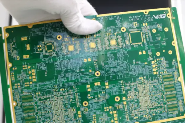
Why is green the universal choice for circuit boards? Behind this seemingly
- Expert en production de petites et moyennes séries
- Fabrication de circuits imprimés de haute précision et assemblage automatisé
- Partenaire fiable pour les projets électroniques OEM/ODM
Heures d'ouverture : (Lun-Sam) De 9:00 à 18:30