

What Documents Are Required for PCB Production: A Field Guide From Real Industrial Weighing Controller PCB Projects
Many engineers focus too much on technical parameters early on and overlook
Hardware Is Where Security Actually Lives
I have always felt that many people’s understanding of network security has drifted off course. They love discussing flashy firewall software or complex encryption algorithm scripts, yet rarely notice the physical foundation that carries all the heavy lifting — that circuit board supporting the entire system. Without a well-designed and reliably manufactured PCB as its backbone, even the most powerful software code is nothing more than a string of characters that cannot run. This is like building a house: having beautiful blueprints does no good — you must first lay a solid foundation.
I have seen many projects compromise on component selection in the early stages to save a little cost, only to encounter endless problems later. Especially when handling massive network traffic, ordinary single-layer or double-layer boards simply cannot hold up under pressure and immediately collapse due to signal interference or thermal management problems. That is when you realize why critical network nodes such as gateway devices must adopt more complex design approaches.
The role of multilayer PCB here is absolutely not simply adding a few more routing layers. It is more like a precision three-dimensional traffic network — rationally separating different functional modules such as the data processing unit, encryption engine, and various interface controllers in three-dimensional space, while ensuring they can work cooperatively at extremely high speeds. This structural advantage simply cannot be replicated by traditional low-layer-count boards. It effectively reduces crosstalk between signals and improves the overall stability of operation.
For example, through dedicated power and ground layers, a clean voltage reference can be provided for sensitive high-speed digital circuits, preventing bit errors caused by power supply noise. Controlled-impedance routing techniques such as microstrip or stripline ensure that high-frequency signals maintain integrity during transmission, reducing reflections and attenuation. Additionally, multilayer boards allow denser component placement and shorter interconnects — critical for encryption operations that demand low-latency processing.
When Eight Layers Was Not Enough: A Real-World Case
We had a project that needed to handle real-time encryption and decryption traffic. The initial design used an eight-layer board, but actual testing found that when concurrent connections suddenly surged, latency became very unstable. We later switched to a specially optimized twelve-layer design. Not only did this resolve the latency problem — overall power consumption also dropped by approximately fifteen percent.
This change appeared to increase upfront manufacturing cost, but considering the stability and maintenance cost over the device’s entire lifecycle, it was actually the more cost-effective choice.
Specifically, the additional layers allowed us to design lower-impedance paths for the power distribution network, reducing voltage fluctuations at chip power supply pins and thereby improving processor stability under full load while reducing energy losses. At the same time, the extra routing layers allowed high-speed signal lines to be sufficiently isolated from noise sources, significantly improving signal quality.
High-Speed Differential Signals: Why They Are So Demanding
The gateway’s core task is to quickly and reliably transfer data packets between network interfaces. This sounds simple, right? But in practice, when you integrate gigabit or even 10-gigabit network ports into the board, you quickly discover how sensitive those high-speed differential signals are.
They place extremely high demands on the integrity of the reference ground plane — any discontinuity causes signal reflections. Trace length even slightly too long or too short affects timing. Too many vias destroy impedance. Even the roughness of copper foil produces losses at high frequencies. When signal rates reach 10 Gbps, the skin effect concentrates current primarily on the conductor surface, and rougher surfaces significantly increase path length and resistance.
A friend’s company learned this the hard way. To save money, they used an ordinary four-layer board for their test prototype. All specifications looked normal. But during mass production, they discovered that high temperature environments frequently caused packet loss. After two months of troubleshooting, the problem was traced to the board material’s dielectric constant changing too much with temperature. At high temperatures, signal propagation speed changed, destroying the strict timing window.
This is why I now place particular emphasis on PCB material selection. For high-frequency applications, low-loss materials like Rogers, while more expensive, provide significantly more stable electrical performance.
Do not assume that materials labeled “industrial-grade” are automatically suitable for your application scenario. Some materials may perform acceptably at room temperature, but their insulation properties or mechanical strength can drop substantially under low-temperature or high-humidity conditions.
Multilayer PCB: What Each Layer Actually Does
Security gateways typically need to operate 24×7 in diverse environments — from constant-temperature, controlled-humidity data center rooms to high-temperature, vibration-prone factory floors. In vibration environments, poor soldering or connector contacts can fail due to fatigue.
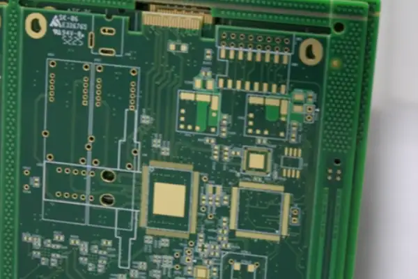
This is where multilayer PCBs show their advantages: you can dedicate middle layers as complete ground planes to shield interference; you can partition the power layer into different zones to provide independent power supply to each module; and you can bury sensitive signal lines in inner layers away from external influence. Routing clock signals on inner layers, for example, effectively reduces outward radiated electromagnetic interference.
But multilayer boards are not a universal solution. More layers means more complex processing, lower yield rates, and naturally higher costs. Even tiny misalignment during lamination can cause uncontrolled impedance.
My general recommendation: first think clearly about what level of protection is actually needed. If it is for home or small office environments, a six-layer board with appropriate layout is often sufficient. For enterprise-grade applications or industrial scenarios, an eight-layer or even ten-layer board is the prudent choice — providing more complete isolation and shielding for critical signals and power supply.
Thermal Design: The Silent Cause of Gradual Failure
Another area many people easily overlook: thermal design on the PCB. Failures caused by poor thermal design tend to be gradual and hard to detect.
Today’s processors consume substantial power — especially those security chips with integrated encryption engines — and the heat generated during operation must be dissipated promptly. Sustained encryption and decryption operations continuously push chip core temperatures upward.
I have seen many designs with all chips packed densely together, resulting in temperatures in the center area running ten-plus degrees higher than the edges. Over extended operation, component aging rates are completely different, and system stability is inevitably affected. Electrolytic capacitors have lifespans that decrease exponentially at high temperatures.
Good practice is to consider thermal paths from the layout stage: high-power chips should be positioned close to board edges or heat dissipation holes; sufficient space should be left between heat-generating devices; when necessary, copper blocks embedded in the PCB can assist heat conduction. Designing thermal via arrays under chip bodies to conduct heat to large copper areas or heatsinks on the reverse side is a common and effective technique.
Power Distribution Network: The System’s Vascular Network
For complex multilayer PCB designs, the power distribution network is like the vascular system of the entire system — it must simultaneously satisfy the differentiated needs of different parts while maintaining overall cleanliness and stability.
Processor cores require low-voltage, high-current power supply. This demands sufficiently low impedance in the supply path — otherwise significant voltage fluctuations occur under large dynamic current changes, directly affecting chip stability. This typically means wider traces, more vias, and a decoupling network composed of capacitors of multiple values placed near power pins to handle current demands from low to high frequencies.
Analog circuits or RF sections are extremely sensitive to noise on the power supply. Even very small ripple may be amplified and affect the performance of the entire circuit. For example, on the supply line of a high-precision ADC or RF transceiver, microvolt-level noise can introduce unacceptable signal distortion or phase noise.
This requires that independent supply channels be planned for these different voltage domains from the design outset, with effective isolation implemented in the physical layout. This isolation is not only electrical — it includes physical spatial separation, such as using splits in the ground layer or isolation zones in the power layer to prevent noise coupling through shared impedance.
Encryption Module Routing: Where Physical Layout Meets Security
Many designs simply place the encryption chip next to the processor and consider the job done. This is not wrong. But what I believe matters more is the quality of the “road” between them — not just how short it is, but whether the surrounding environment is noisy. Is there a high-frequency switching power supply buzzing nearby? Is there a high-speed bus running beneath?
These details are what truly determine whether your key transmission will encounter problems.
In practice, encryption data lines should be routed in dedicated microstrip or stripline channels fully enclosed by ground planes, with strictly controlled impedance. Embedded capacitance technology can even be considered, embedding discrete capacitors between power-ground plane layers directly beneath the routing to provide the shortest possible discharge path for high-frequency noise — ensuring waveform integrity during transmission and avoiding encryption errors caused by signal distortion.
Management Interfaces: The Side Doors Most Easily Overlooked
Everyone focuses on high-speed signals — DDR routing, differential pair matching — and these certainly matter. But an area easily overlooked is those seemingly “low-speed” management interfaces: a debug serial port or a management Ethernet port.
Think about it: if these areas lack proper isolation protection and someone injects a high-voltage pulse from the outside, the entire system could potentially be paralyzed.
So now in my designs, even next to the simplest RS232 interface, I always add TVS devices and isolation components. For management Ethernet ports, I also use PHY chips with isolation transformers and add common-mode chokes in front of the transformer to resist common-mode surges from lightning induction or electrostatic discharge. These interfaces are often the “side doors” most easily accessible to attackers. Their protection level must equal or exceed that of core business interfaces.
Finding the Right Manufacturing Partner
True reliability cannot be guaranteed by a certification certificate. I have seen many manufacturers with comprehensive certifications whose actual production processes had no effective traceability. When a quality issue appeared, there was no way to trace which process step had failed.
I am far more willing to visit a factory, observe the operations on the production line, and look at how workers handle defective products. Once when evaluating a potential PCB supplier, their workshop had a whiteboard that recorded in detail the problems that had occurred in production over the past week, the corresponding corrective measures, and specifically which machine and which operator was involved. That kind of transparency and attitude toward problems gave me more confidence than any certificate.
I remember when we were working on an intelligent gateway project last year. We approached a large factory that claimed to have supplied Huawei. Their CPK data was impeccably beautiful and they had certificates covering every table. But the first batch of boards came back with problems — impedance deviations or layer misalignment. We later found out their engineers had not carefully reviewed our lamination design and had simply followed a standard template.
The company that actually helped us solve the problem was a much smaller one. The owner personally brought their engineers and met with us three times, going through our multilayer PCB design from beginning to end, raising several suggestions we had not thought of — such as adjusting the ground plane layout on two of the layers to reduce crosstalk. They did not have impressive credentials, but their obsessive attention to detail gave us real confidence.
This “obsessive attention to detail” often shows up in easily overlooked areas. For instance, a supplier with real experience will proactively suggest using back-drilling to optimize via stub effects for high-speed applications. Or they may recommend specific low-loss dielectric materials like Panasonic’s MEGTRON series based on your signal rates and thermal dissipation requirements, rather than defaulting to FR-4. These recommendations grounded in real engineering experience often determine final product performance and reliability more than following standard processes.
The Balance: Complexity, Reliability, and Cost
I recently explored what happens when complex AI inference modules are integrated directly into existing gateway architectures. The idea was to make edge devices smarter — capable of judging threats themselves.
The result: to power and cool that high-performance SoC, the multilayer PCB layer count was pushed to eighteen or more. Routing satisfied signal integrity requirements. But the board became thick and rigid, more prone to problems in industrial environments with vibration or large temperature variations. Solder joint fatigue, subtle inner-layer delamination — these issues all emerged.
So I now lean toward a different approach: rather than squeezing everything onto one board and causing “bloat,” consider a more flexible modular design. The core switching and routing functions can be implemented on a relatively stable, proven multilayer PCB platform — perhaps ten to fourteen layers. The AI processing unit that needs rapid iteration and updates can be made into a separate, pluggable daughter card. That way the main board’s complexity is controlled, and the intelligent analysis card can quickly adopt newer versions as algorithms evolve.
For most practical enterprise-level gateway scenarios, data flows are not running at maximum speed continuously. They are more often in a “burst” state. Mixed material structures can be considered — using high-performance materials only beneath the most sensitive high-speed differential pairs for signal quality, while the majority of the board uses more cost-effective FR4 with better processability. After optimization, not only does cost come down — yield rate and reliability are also more readily guaranteed.
Security that is truly hardware-based should not be an isolated “module” soldered onto the board and considered complete. Real physical tamper protection should be a design philosophy running through the entire system — for example, a carefully designed routing layout can form an invisible detection grid where any attempt to probe or intrude will change the electrical characteristics of that region, allowing the system to detect it. This protection mechanism deeply integrated into the multilayer PCB’s interior is more hidden and harder to bypass than adding a standalone encryption chip.
Ultimately, the core competitiveness of security gateways may not lie entirely in how “high-tech” the board itself is — but in how clever system architecture design allows all components including the multilayer PCB to work together: maintaining sufficient performance and forward-looking capability while ensuring long-term robustness in actual deployment environments. After all, for the gatekeeper, standing firm matters more than jumping high.
Many engineers focus too much on technical parameters early on and overlook
As someone who has worked in PCB outsourcing for years, I’ve found
Cramming a camera, amplifier, dual-mic array, and Wi-Fi radio into a palm-sized
- Expert en production de petites et moyennes séries
- Fabrication de circuits imprimés de haute précision et assemblage automatisé
- Partenaire fiable pour les projets électroniques OEM/ODM
Heures d'ouverture : (Lun-Sam) De 9:00 à 18:30
Get quote, solution or any question, Andre always here to help