
Why does your Motor Drive PCB always “retire” early?
The motor drive circuit board in industrial equipment failed after long-term operation,
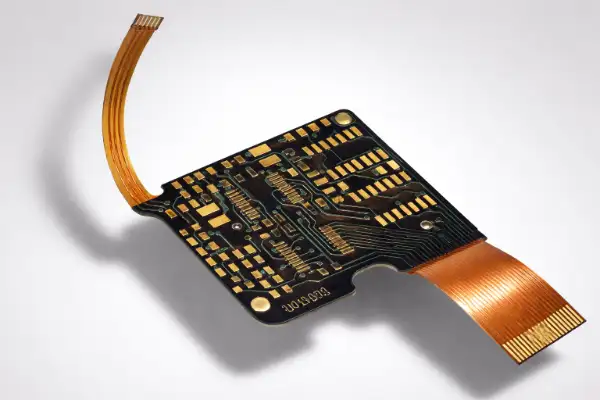
I recently conducted research into a specialized type of circuit board design, only to discover that many people’s understanding of it remains superficial. This approach—which integrates both rigid and flexible components—effectively resolves many of the pain points associated with traditional circuit boards.
I recall seeing the internal design of a smartwatch that utilized this rigid-flex solution. Initially, I assumed the purpose was simply to make the device thinner and lighter; however, I later realized that its bending performance was the true critical factor. Since a watch is worn on the wrist, it is constantly in motion; a standard circuit board would easily fracture under such repeated bending stress. This specialized design, however, allows the circuit board to remain flexible in areas where bending is required, while maintaining rigid support in other sections.
The testing phase often serves as the ultimate litmus test for the quality of a design. I have witnessed products undergoing rigorous bending tests in laboratory settings, where every single flex cycle must be verified to ensure that electrical connections remain completely unaffected.
These tests are not merely performed a few times for the sake of formality; rather, they are designed to simulate usage scenarios spanning several years—or even longer—to ensure long-term reliability.
Today, many electronic products strive for thinner and lighter designs—a trend that presents new challenges for circuit boards. A singular focus on miniaturization can often come at the expense of reliability; the rigid-flex design, however, strikes a perfect balance between these two competing demands. For instance, in wearable devices—which require both wearer comfort and the stable operation of internal components—this type of circuit board excels at satisfying these seemingly contradictory requirements.
In fact, this design philosophy is quite common in our everyday lives. Consider our own fingers: they possess hard bones to provide structural support, yet feature flexible joints that enable fluid, agile movement. Effective engineering design often follows this principle: rather than blindly pursuing a single extreme, it seeks to identify the optimal balance point.
I have noticed that some manufacturers, in their quest for ultimate thinness and lightness, inadvertently overlook issues regarding reliability in real-world usage. This reminds me of some early foldable smartphones, where flaws in the hinge-area circuit design led to screen malfunctions. However, with the adoption of a sensible “rigid-flex” hybrid design, such issues have been significantly mitigated.
Ultimately, any technology must serve practical needs. We should not adopt new technologies merely for the sake of using them; rather, we must clearly discern exactly what problems they are capable of solving. The reason this particular type of circuit board design is gaining such widespread popularity is precisely because it genuinely offers superior solutions across a multitude of scenarios.
I have always felt that the most fascinating aspect of the electronics industry lies in how seemingly contradictory design concepts can be seamlessly integrated. Take, for instance, the ubiquitous circuit board: traditional rigid boards are too inflexible, while purely flexible boards lack structural support. It wasn’t until I encountered the rigid-flex printed circuit board that I truly understood what it meant to strike the perfect balance.
I recall a project last year involving a wearable device for a client; we decided to place the sensor modules within the rigid sections while utilizing a flexible design for the connecting segments. This hybrid approach—combining rigid and flexible elements—allowed the product to maintain structural stability while simultaneously delivering a comfortable wearing experience. What astonished me most was the device’s exceptional reliability during rigorous bending tests—a performance that completely revolutionized my understanding of circuit board durability.
The challenges encountered during the manufacturing process are, in reality, far more numerous than one might imagine. On one occasion, a prototype sample exhibited delamination issues; we later discovered that the transition zone between the rigid and flexible sections had not been treated with sufficient precision. Such minute details often determine the ultimate success or failure of a product, necessitating that manufacturers possess a profound understanding of material properties. I have encountered far too many teams that focus exclusively on circuit design while neglecting the critical aspect of physical structural compatibility.
Today, one can observe traces of this design philosophy in a great many innovative products. Consider, for instance, the recently popularized foldable devices, whose internal interconnections ingeniously leverage rigid-flex technology. This reminds me that the evolution of electronic products mirrors biological evolution—it is a perpetual quest for the optimal structural solution.
In practice, when selecting this type of circuit board material, one cannot rely solely on technical specifications. My customary approach is to first gain a thorough understanding of the product’s actual usage scenarios: Will it be subjected to frequent bending, or will it maintain a fixed form? Will the operating environment involve temperature fluctuations or mechanical vibrations? These factors all play a critical role in determining the optimal ratio and configuration of the rigid and flexible zones.
Sometimes, true innovation lies precisely within these points of convergence. When we cease to view a printed circuit board merely as a two-dimensional plane and instead perceive it as an integral part of a three-dimensional structure, our design philosophy undergoes a complete transformation. This, perhaps, is the most captivating aspect of electrical engineering—the constant quest to discover a point of equilibrium amidst seemingly contradictory characteristics.
I have encountered numerous engineers who adopt an overly conservative approach to the design of rigid-flex PCBs. They often harbor the misconception that the flexible sections must be completely encased or concealed to ensure safety—a belief that is, in fact, a fallacy.
I recall a medical device project from last year that left a lasting impression on me: the client insisted on densely populating the bend zones of the rigid-flex PCB with vias to enhance structural stability. The result? Every single unit in the initial batch of prototypes failed during durability testing due to breakage.
The root of the problem lay precisely in a misunderstanding of the very concept of “flexibility”—true durability stems from a rational distribution of mechanical stress, not from excessive reinforcement.
Drilling processes, for instance, serve as a critical litmus test for one’s design philosophy. Some designers prefer to arrange vias in a uniform pattern along the interface between the rigid and flexible sections; counterintuitively, this creates mechanical weak points.
A far more rational approach involves positioning vias at least 3 millimeters away from the bend line and arranging them in a staggered pattern—effectively outfitting the circuit board with a suit of elastic armor.
Another easily overlooked detail concerns the dynamic adjustment of drilling parameters for rigid-flex boards. As the drill bit penetrates the rigid layer and enters the flexible layer, the spindle speed must be reduced by approximately 20% to ensure the integrity of the hole walls—a process that demands an almost intuitive understanding of material properties from the machine operator.
I strongly advise newcomers to pay close attention to the inherent properties of their board materials. Certain substrates marketed as “highly flexible” may, in reality, withstand fewer bend cycles than standard polyimide materials. It is akin to buying running shoes: one cannot simply judge their quality by the thickness of the sole; one must actually try them on and take a few steps.
I recently tested a fascinating design concept utilizing a three-layer asymmetric structure. By positioning the thickest rigid layer on the outer side of the bend radius, we were able to boost the board’s fatigue life by a remarkable 30%. Such counter-intuitive approaches often pave the way for groundbreaking innovations.
The true measure of engineering mastery lies in those invisible details—such as using a UV laser to etch microscopic grooves into the flexible sections to precisely guide the flow of mechanical stress. This technique proves far more effective than simply increasing the overall thickness of the board material. Sometimes, the simplest solutions prove to be the most effective. In one particular drone project, for instance, simply replacing sharp right-angle bends with smooth, curved transitions allowed the prototype to pass 20,000 dynamic stress tests with flying colors. Truly good design should flow naturally around obstacles, much like water.
If you are currently working on this type of design, I suggest giving this method a try: start by 3D printing a full-scale (1:1) model and repeatedly bending it by hand. The tactile feedback you get from a physical object will often reveal potential issues much sooner than any computer simulation ever could.
I’ve recently been researching the design of various electronic devices and have observed a rather interesting phenomenon. Many engineers, when designing products, face a classic dilemma: how to ensure circuit stability while simultaneously maintaining the device’s overall flexibility.
I recall once disassembling a fitness tracker; the design of its internal circuit board left a lasting impression on me. It utilized a “rigid-flex” printed circuit board structure—a hybrid approach that provided the necessary structural rigidity for support while allowing for natural, fluid bending in the specific areas where flexibility was required. This design philosophy reminded me that, in engineering, the best solutions are rarely a matter of choosing one extreme over the other.
The use of polyimide material represents a truly pivotal breakthrough in this regard. Its inherent flexibility allows circuit boards to be folded and unfolded—much like turning the pages of a book—without compromising their electrical conductivity. I have personally seen test samples that remained fully functional and intact even after enduring tens of thousands of bending cycles.
However, in practical applications, I’ve discovered that blindly pursuing maximum flexibility isn’t always the optimal strategy. In fact, designs that place excessive emphasis on flexibility can sometimes inadvertently create a new set of problems.
For instance, in devices that require frequent disassembly and reassembly, an overuse of flexible connections can lead to premature wear and tear at the connection points.
The design philosophy I personally subscribe to is one that seeks a harmonious balance between rigidity and flexibility. It mirrors the relationship between bones and joints in the human body: providing sufficient structural support while simultaneously ensuring the freedom and flexibility of movement.
Some of the smartwatches I’ve seen recently exemplify this principle beautifully. They incorporate flexible circuitry at the watchband junctions—the areas requiring movement—while maintaining a rigid structural framework for the main body of the device.
This design philosophy, in fact, has the potential to be applied across a much broader spectrum of fields.
I believe the future trajectory of electronic device development lies in seamlessly integrating technology into our daily lives in the most natural way possible. And it is precisely this blend of rigid and flexible circuit design that makes such integration a tangible reality.
I’ve always found the process of selecting a supplier for rigid-flex PCBs to be quite an intriguing experience. Many people jump straight to asking about pricing or obsessing over how impressive the numbers look on a technical data sheet. Yet, in reality, those metrics are merely scratching the surface. The key factors that truly determine whether a circuit board will perform satisfactorily and endure over time often lie hidden in the details.
A project I worked on last year serves as a particularly illustrative example. At the time, we required a rigid-flex printed circuit board capable of undergoing repeated bending within a confined space. After engaging with several suppliers, we observed an interesting phenomenon: some manufacturers focused entirely on showcasing the sheer volume of imported equipment they possessed, whereas a slightly smaller supplier devoted a significant amount of time to discussing—with us—the product’s bending frequency and the range of environmental temperature fluctuations it would encounter during actual use.
This disparity directly impacted the subsequent collaborative experience. The supplier willing to delve deeply into understanding our specific application scenario eventually became our long-term partner. Their engineers even proactively alerted us to potential stress concentration issues at certain connection points—which might have exceeded our initial expectations—and recommended incorporating reinforcement patches into the rigid sections of the design.
In my view, an excellent supplier should function as an attentive partner rather than merely a fabrication facility. They must grasp that the junction between rigid and flexible sections constitutes not merely a physical connection, but a functional complementarity. Occasionally, I deliberately pose seemingly simple questions—such as, “Why was this specific thickness selected for the material in this transition zone?”—primarily to discern whether the supplier is simply reciting standard protocols or can articulate the actual engineering trade-offs and considerations involved.
Currently, there is an unfortunate trend within the industry where manufacturers place excessive emphasis on pushing technical parameters to their absolute limits, while simultaneously neglecting a product’s capacity to adapt to real-world operating environments. I have witnessed far too many instances where the over-optimization of a single metric resulted in a decline in overall reliability—a classic case of putting the cart before the horse.
Truly valuable collaboration should be a reciprocal process in which both parties draw insights from their respective experiences, fostering mutual growth.
While recently researching circuit board design, I stumbled upon a rather intriguing observation. Many people assume that circuit boards intended for medical devices should be as rigid and robust as possible; in reality, the exact opposite is often true. Devices designed for implantation within the human body frequently require greater flexibility and adaptability—much in the same way a vascular stent must gently expand and contract in rhythm with the patient’s pulse.
I recall a conversation with an engineer specializing in cardiac pacemakers; he mentioned that their primary design challenge was not ensuring the circuit board’s structural strength, but rather finding ways to render it more pliable without compromising its functional integrity. This brought to mind the flexible plastic rulers I used to play with as a child—only now, that same underlying principle is being applied within a far more sophisticated and critical technological domain.
Indeed, an increasing number of medical devices today are incorporating materials that possess this dual capability: maintaining a specific structural form while simultaneously allowing for appropriate degrees of flexibility. Imagine if an implanted medical device were completely rigid; every time a muscle contracted, it would generate friction—a burden that, over the long term, would prove detrimental to the patient.
I once encountered a particularly intriguing design that ingeniously combined rigid and flexible components—much like the foldable smartphones we use in our daily lives. The rigid sections served to house the primary chips, while the flexible sections acted as bridges, connecting the various modules. This design philosophy broke free from the traditional dilemma of circuit boards, which typically forced a binary choice between being either entirely rigid or entirely flexible.
A friend of mine, who works on fitness tracking wristbands, told me that their team had tested nearly 50 different material combinations. They ultimately discovered that—contrary to intuition—softer isn’t always better. The key lies in finding that delicate balance: the device must be flexible enough to withstand the bending and flexing associated with daily activities, yet rigid enough to ensure the stability of its electrical connections.
In fact, this line of reasoning applies to other fields as well. Wearable technology, for instance, requires a careful balance between comfort and durability; if a device is too rigid, it becomes uncomfortable to wear, but if it is too flexible, it becomes prone to damage. This reminds me of the principles of seismic design in architecture: a structure must possess sufficient rigidity to withstand the forces of an earthquake, yet retain enough flexibility to absorb and dissipate that energy.
I believe that, in the future, this design philosophy—which harmonizes rigidity with flexibility—will become increasingly prevalent. After all, our lives are inherently a blend of the rigid and the flexible; why shouldn’t the tools we use reflect that very nature?
I have long felt that when discussing rigid-flex circuit boards, people often get bogged down in comparing technical specifications while overlooking the underlying design logic behind the choice of materials. I once observed an engineer in a laboratory repeatedly bending two different samples: the substrate of the “adhesive-free” structure curled naturally, much like the page of a book, whereas the substrate containing adhesive consistently developed fine creases at the exact same points. That visual contrast gave me a sudden, profound insight into the fundamental differences between the materials themselves.
Traditional substrates that rely on adhesives are akin to forcibly gluing together materials with disparate properties; in high-temperature environments, the increased molecular activity within the adhesive layer can compromise the stability of the dielectric medium. I have seen flexible circuits—specifically those utilizing adhesive-free solutions in medical devices—retain their original form even after enduring hundreds of high-temperature steam sterilization cycles. In contrast, the copper foil edges of adhesive-based materials would begin to show signs of fine blistering. This disparity becomes significantly amplified within precision instrumentation; since every dielectric layer along a signal transmission path contributes to the formation of the electromagnetic field, a non-uniform medium like an adhesive acts much like pouring murky sediment into a crystal-clear stream. The superiority of rolled copper lies not merely in its physical properties. During one instance of disassembling the wiring within an industrial robotic arm’s joints, I discovered that the flexible sections utilizing rolled copper remained as smooth as new—even after enduring tens of millions of extension-retraction cycles—whereas the surfaces of sections made from electrolytic copper were already riddled with microscopic cracks. This disparity stems from the specific arrangement of the metal’s crystalline grains: the rolling process aligns the grains in an orderly fashion along the direction of tension—much like tightly woven fibers—whereas the random grain structure formed by electrolysis resembles loosely piled gravel. When a circuit board is required to undergo repetitive motion in tandem with a device’s joints, this structural advantage translates directly into an extended operational lifespan.
The true test for rigid-flex printed circuit boards lies in dynamic operating environments. Circuit boards within automotive radar systems, for instance, must simultaneously withstand the extreme thermal shock of the engine compartment and the mechanical vibrations of the vehicle chassis; with conventional substrate materials, the risk of delamination frequently manifests at the transitional interface between the rigid and flexible zones. Last year, while participating in a satellite project, I observed how space-grade rigid-flex boards—operating in a vacuum—had to contend with temperature fluctuations spanning hundreds of degrees (both positive and negative). Those components featuring a “glue-free,” monolithic structure passed the thermal cycling tests flawlessly, precisely because the coefficient of thermal expansion formed a continuous gradient extending from the polyimide substrate to the copper foil.
Fundamentally, the selection of materials constitutes a choice regarding design freedom. When I observed the sinuous, winding circuit board inside a smartwatch—effortlessly threading its way through the confined space of the watchband hinge—I became even more convinced that miniaturization is not merely a pursuit of thinner dimensions; rather, it is a process of unlocking new possibilities for product innovation.
I have encountered quite a few engineers who find the design of rigid-flex printed circuit boards to be a particular headache. They often perceive these boards as an inherent contradiction—requiring them to simultaneously ensure the structural stability of the rigid sections while accommodating the bending flexibility of the flexible sections. In reality, the key lies in understanding material properties rather than getting bogged down in rigid adherence to specific parameters.
I recall a project that required implementing a circuit-folding function within a confined space. At the time, we abandoned the traditional multilayer PCB approach in favor of a rigid-flex design. The conformity of the flexible section was truly impressive; it bent as naturally as the pages of a book without generating any stress concentrations.
The etching process plays a pivotal role here. Many assume that simply making the circuit traces thinner is sufficient; however, etching parameters must actually be adjusted based on the varying copper thickness in different regions. On one occasion, we encountered persistent trace breaks in the flexible sections; we later discovered that the etching duration had not been independently controlled to account for the material differences between the rigid and flexible zones.
The true technical challenge lies in achieving a seamless transition between the rigid and flexible sections. It is akin to tailoring a garment for a circuit board: the seams must be secure, yet they must not compromise the flexibility of the moving joints. We experimented with various prepreg flow rates before ultimately selecting a low-flow material, ensuring that during the lamination process, the resin would not bleed into unintended areas.
What left the deepest impression on me was the coverlay lamination stage. Both temperature and pressure had to be precisely regulated across different zones—much like balancing the distinct needs of both the elderly and children simultaneously. The rigid sections required sufficient pressure to ensure strong adhesion, while the flexible sections demanded a gentler touch to prevent deformation of the thin film.
Ultimately, the most fascinating aspect of these boards is their ability to transcend the planar limitations of traditional PCBs. You can roll them into a cylinder or fold them into a Z-shape, opening up entirely new possibilities for product design. On one occasion, we even engineered a circuit board into a retractable spring structure—something utterly unimaginable with standard PCBs.
Looking back now on those days spent fine-tuning parameters, the effort—though arduous—was undoubtedly worthwhile. After all, achieving that delicate balance between structural durability and operational flexibility in electronic devices is an art form that cannot be mastered overnight.
I have always found the fabrication of rigid-flex boards to be a particularly fascinating process. I recall that when I first attempted to build one, I completely overlooked the specific characteristics of the copper foil; consequently, during the testing phase, I heard the faint sound of traces snapping. It was only then that I fully grasped just how critical the proper selection of materials truly is.
Rolled copper foil is, indeed, far better suited than traditional materials for applications involving repeated bending. Its surface is exceptionally smooth—possessing a texture akin to silk—which effectively disperses stress across the material during multiple bending cycles. Through comparative testing, I discovered that under the same number of bending cycles, ordinary materials would have long since developed fine cracks, whereas rolled copper foil remains intact.
However, what many people tend to overlook is that—beyond the material itself—the approach taken during the design phase is equally critical. For instance, particular attention must be paid to the transition zones between rigid and flexible sections; I typically prefer to incorporate curved contours in these areas rather than sharp right-angle turns. On one occasion, a client requested an exceptionally thin rigid-flex printed circuit board, which subsequently led to issues at the bending points. We eventually found the optimal balance between the copper foil thickness and the bending radius.
The bending angle also requires careful consideration. Some designers, in pursuit of an ultra-compact folding profile, opt for an extremely tight bending radius; paradoxically, this often compromises the product’s service life. I have found that incorporating a moderate curvature not only enhances the product’s durability but also improves its tactile feel during actual use.
A recent smartwatch project successfully applied this philosophy. At the watchband connection points, we deliberately allocated ample space for bending; although the aesthetic might not appear quite as “extreme,” the device continued to function flawlessly even after enduring tens of thousands of bending cycles during testing. Such design trade-offs are often far more critical than the mere pursuit of extreme technical specifications.
In truth, after years of experience, one realizes that a well-designed rigid-flex PCB is akin to a dance performance—it requires a harmonious interplay between rigidity and flexibility. The true test of technical expertise lies in striking that delicate balance between ensuring circuit stability and maintaining operational flexibility.
Whenever I encounter circuit boards that have been mangled beyond recognition by repeated bending, I feel that the designers have treated these rigid-flex boards merely as standard rigid PCBs. I have witnessed countless instances where a failure to account for stress distribution resulted in broken traces, causing the product to fail within less than six months of use.
The greatest nemesis of rigid-flex PCBs is the fatigue damage induced by repetitive bending. Many designers assume that simply making the flexible section thinner is sufficient; however, the true key lies in the layout strategy of the traces. I typically route critical traces in a curved pattern as they traverse the bending zones. Straight-line routing, conversely, creates distinct points of stress concentration when subjected to repeated bending.
I recall a particularly memorable smartwatch project where the initial design placed the power lines and signal lines side-by-side along the exact same bending axis. Testing subsequently revealed that every wrist-flicking motion subjected the copper foil at specific locations to excessive tensile stress.
We subsequently revised the routing paths, ensuring that the critical signal lines were routed to bypass the areas subjected to the maximum bending radius. Simultaneously, an interleaved routing strategy is employed across different layers to effectively distribute mechanical stress.
The handling of transition zones is often underestimated. Many assume that simply adding a stiffener is a cure-all solution. In reality, the root cause lies in the inherent differences in the elastic moduli of the materials themselves. I prefer to design a buffer zone situated between the rigid and flexible sections; within this region, the copper thickness should transition gradually.
A medical endoscope project I worked on recently serves as an excellent example of this approach. The device required undergoing hundreds of bending and sterilization cycles every day. To accommodate this, we implemented a specialized, wave-shaped routing pattern at the connection points.
The true test of a rigid-flex PCB designer’s expertise lies in dynamic application scenarios. Static bending applications merely require consideration of the board’s final, formed position. However, for components such as the hinges found in foldable smartphones, each rigid-flex board must withstand the rigorous challenge of tens of thousands of bending cycles.
In my experience, it is best to avoid placing vias within the bending zones whenever possible; vias essentially create a “backdoor” for stress to concentrate.
Sometimes, the simplest solutions prove to be the most effective. For instance, slightly increasing the thickness of the flexible substrate can significantly enhance its bending durability—though this may come at the cost of some flexibility.
Ultimately, designing rigid-flex PCBs is an iterative process that necessitates continuous trial and error. A practice I particularly admire involves conducting accelerated life testing during the prototyping phase. After all, even the most sophisticated computer simulations cannot replicate the tangible insights gained from actual physical bending tests.
I have always found flexible circuit boards—those that can bend and flex—to be particularly fascinating. Unlike conventional PCBs, which remain rigid and static in a fixed location, their inherent flexibility opens up a vast array of new possibilities for electronic product design.
I recall once examining the internal architecture of a fitness tracker. It utilized a PCB design capable of simultaneously maintaining a specific form factor while allowing for flexible movement. The most ingenious aspect was the routing layout connecting the display to the main board; rather than simply bunching the traces together in a straight line, the designers employed a serpentine routing pattern. This approach effectively distributed the mechanical stress across the circuit as the user moved their wrist.
The primary challenge in this type of design lies in simultaneously ensuring signal transmission stability while mitigating the cumulative wear and tear caused by repeated bending. I have encountered products where, in the pursuit of a slimmer and lighter profile, the interconnect sections were oversimplified—resulting in intermittent connection issues after only a short period of use.
In truth, the success of these flexible circuit boards hinges most critically on the harmonious interplay between material selection and manufacturing processes. The materials used in different sections of the board must integrate seamlessly to guarantee stable overall performance. Sometimes, even a minuscule difference in thickness can impact the entire product’s lifespan.
Many wearable devices today utilize this technology, yet I feel that truly well-executed implementations are few and far between. To cut costs, some manufacturers skimp on materials in critical areas, resulting in products that simply cannot withstand the rigors of daily use.
Good design, in my view, entails simplifying the structure as much as possible—while ensuring full functionality—by eliminating unnecessary layers and maximizing the utility of every single component. This is where an engineer’s true expertise is put to the test.
When designing electronic products, many people fall into a common trap when selecting rigid-flex PCBs: they assume that simply using this type of board guarantees a trouble-free outcome. In reality, different grades of rigid-flex printed circuit boards vary significantly in terms of durability. I have seen far too many instances where a product failed prematurely simply because the wrong grade of board was selected.
I recall a team developing a smartwatch that, in an initial effort to save costs, opted for a lower-grade PCB. Consequently, less than six months after the product hit the market, they were inundated with complaints regarding broken display cables. It wasn’t until they went back to redesign the product that they pinpointed the root cause: a mismatch in materials within the flex zone. Without a properly engineered transition between the flexible and rigid sections, repeated flexing causes mechanical stress to concentrate within an extremely small area.
This brings to mind the industry’s classification standards for product reliability. Class 1 PCBs are indeed inexpensive, but they may not even survive 10,000 flex cycles. In contrast, Class 3 PCBs—the grade typically used in high-end medical equipment—can achieve a flex life in the range of millions of cycles thanks to specialized processing techniques. This disparity lies not merely in the materials themselves, but more importantly, in the precision and control exercised throughout the entire manufacturing process.
During a factory tour on one occasion, an engineer showed me a fascinating comparison. They had simultaneously tested two rigid-flex PCBs that appeared identical on the surface: one produced using standard manufacturing processes, and the other utilizing a specialized copper foil treatment technique. Under identical flex-testing conditions, the standard board began to exhibit micro-cracks after approximately 30,000 cycles, whereas the optimized board remained completely intact even after completing 100,000 cycles.
The true test of a rigid-flex PCB’s performance often lies in those invisible details—such as the uniformity of the copper foil thickness in the flexible zone, the proper matching of the coverlay’s elastic modulus, and the appropriateness of the bending radius. Collectively, these factors determine whether the circuit board can withstand the mechanical stresses associated with long-term use.
Consequently, whenever I now evaluate a new rigid-flex design proposal, I place a much greater emphasis on its dynamic performance data. No matter how impressive static specifications may appear, they are never as intuitive as actual bending tests. After all, the true lifespan of an electronic product must ultimately be validated within real-world usage scenarios.
I have always felt that the most fascinating aspect of electronic product design lies in those invisible details. Take the mobile phones we use every day, for instance: many people may not realize that what truly determines a product’s longevity is often found in its most inconspicuous connection points. I recall once disassembling an old phone for repair, only to discover that the point of failure was neither the motherboard nor the screen, but rather a flexible ribbon cable that had been subjected to repeated bending. This experience sparked my interest in the field of rigid-flex printed circuit boards.
Traditional design paradigms tend to treat circuit boards and connectors as separate entities; however, in practical application, one quickly discovers that every additional interface introduces a corresponding increase in the risk of failure. I have seen far too many devices prematurely rendered obsolete due to loose connectors or severed ribbon cables. This is precisely where the value of a rigid-flex printed circuit board becomes apparent—it seamlessly integrates the rigid and flexible components into a single, unified assembly.
Interestingly, the primary technical challenge in this design approach lies not in the materials themselves, but rather in managing the mechanical stress at the junctions where different materials meet. It is akin to bonding a steel bar to a rubber band: when bent, the point of greatest stress concentration occurs precisely at that interface. During a factory tour, an engineer once showed me samples under a microscope; the specially treated transition layers appeared as exquisite and intricate as works of art.
Today, this technology is being widely adopted in various smart wearable devices. For instance, circuitry can be directly embedded within the wristbands of fitness trackers, thereby conserving space while simultaneously enhancing overall reliability. Compared to older solutions—which relied on separate ribbon cables to link the motherboard to sensors—this integrated approach represents a significant leap forward in terms of both structural integrity and durability. That said, this design methodology does impose more stringent requirements on manufacturing processes, necessitating particular attention to the bending endurance of the flexible components.
In terms of specific application scenarios, I believe the ultimate test of this technology lies in components that undergo repetitive motion. Examples include the hinge mechanisms of foldable smartphones or the internal wiring within the joints of industrial robots—applications where standard circuit boards simply cannot withstand tens of thousands of bending cycles. In such contexts, the advantages of rigid-flex technology become exceptionally pronounced: it ensures consistent electrical performance while simultaneously adapting to dynamic operational environments.
Ultimately, from the perspective of user experience, the greatest benefit conferred by this technology is that it makes devices far more robust and resilient. Whereas users previously harbored concerns that frequent opening and closing might damage their devices, products incorporating rigid-flex designs now offer a significantly greater sense of reassurance. After all, with so many fewer connectors and interconnects, the potential points of failure are naturally reduced.
However, if I had to name the application case that impressed me the most, it would have to be equipment used in certain specialized fields—for instance, medical probes designed to penetrate deep inside the human body, or inspection instruments operating in harsh environments. The circuit boards in these devices must not only guarantee precision but also withstand rigorous tests involving various forms of physical deformation. It is in such scenarios that one can truly appreciate a designer’s mastery in balancing rigidity with flexibility.
Ultimately, good engineering design should solve problems in precisely this unobtrusive manner. Users need not be aware of the specific technologies employed internally; what matters is that they can tangibly experience a product that is more reliable and easier to use. This is arguably where rigid-flex technology offers its greatest value—it ensures that complex engineering ultimately serves the purpose of delivering a simple, seamless user experience.
While recently researching electronic product design, I observed an interesting phenomenon: many engineers still view rigid-flex PCBs merely as a “premium alternative.” In reality, this perspective is far too narrow. I recall that last year, while designing a wearable device, our team initially experimented with a traditional approach combining rigid boards with flexible ribbon cables. However, during the testing phase, we discovered that those tiny connectors were particularly prone to failure; even the slightest vibration of the device would cause the signal to become intermittent.
We subsequently switched to an integrated rigid-flex printed circuit board design, which finally resolved the issue. The true brilliance of this design lies in its ability to unify the rigid and flexible sections into a single, cohesive entity. You no longer have to worry anxiously about the fragility of those external connectors. The entire circuit routing is completed internally—much like constructing a dedicated “expressway” exclusively for the electronic components. This design not only eliminates the signal loss typically associated with connectors but also significantly enhances the product’s mechanical durability. For instance, in devices like smart wristbands that undergo frequent bending, a rigid-flex PCB can withstand tens of thousands of flex cycles without any degradation in performance. Furthermore, by reducing the number of connectors and interconnects, the overall weight can be reduced by approximately 30%—a critical advantage for wearable devices where lightweight design is a primary objective.
I am particularly captivated by the design of the transitional zones where the rigid and flexible sections meet—specifically, the way they feature a gradual, seamless transition. This design approach preserves the structural stability of the rigid regions while simultaneously allowing the flexible sections to bend freely. This design philosophy offers us a profound insight: why must we always confine ourselves to an “either/or” mindset? After all, much like in life itself, many things require the wisdom of balancing both rigidity and flexibility. In terms of manufacturing processes, this transitional zone typically employs a layered stack of specialized dielectric materials. By precisely controlling the thickness and elastic modulus of each individual layer, a smooth transition in mechanical properties is achieved. Engineers blend materials in varying proportions—much like mixing a cocktail—to allow the rigid section to gradually “soften” into the flexible section.
Looking back now at designs that still rely on traditional connector solutions, it feels as though they are merely using glue to paste two separate worlds together. Although they appear to be joined, a fundamental disconnect—a barrier—persists between them. True rigid-flex integration, however, achieves a genuine fusion at the very material level; the difference is akin to that between a forced, cobbled-together collaboration and a truly cohesive, high-synergy team. Take mobile phone camera modules as an example: traditional designs require multiple connectors to link the sensor, lens, and mainboard, whereas a rigid-flex PCB allows the camera module and mainboard to be fabricated as a single, unified entity. This not only conserves precious internal space but also eliminates signal integrity issues often caused by connector oxidation.
Sometimes I reflect on how the evolutionary trajectory of electronic products mirrors our own approach to problem-solving. Initially, we tend to break down complex systems into multiple simpler components, subsequently using various means to connect them. Yet, the weakest links often emerge precisely at these connection points. We eventually come to realize that the truly elegant solution lies in allowing these disparate parts to merge naturally into a unified whole. This design philosophy is particularly evident in the aerospace sector. Electronic systems aboard satellites must withstand extreme temperature fluctuations and intense vibrations; by eliminating connection points, rigid-flex PCBs significantly enhance system reliability. Every connector represents a potential point of failure; an integrated design, conversely, is akin to transforming a scattered group of soldiers into a tightly coordinated special operations squad.
Of course, rigid-flex boards are not a universal panacea; they demand a more refined design approach and sophisticated manufacturing processes. However, this integrated mindset truly opens up new possibilities for us—particularly in the realm of modern electronic devices, where the pursuit of miniaturization, slim profiles, and high reliability is paramount. You will find that this design philosophy is being adopted with increasing frequency. For instance, in medical implantable devices, rigid-flex boards can conform perfectly to the contours of the human body while simultaneously ensuring the stable operation of electronic components. Designers must act much like tailors, custom-fitting the ratio of rigid to flexible sections and the bending radius for each specific application—a task that necessitates the integration of knowledge across multiple disciplines.
Ultimately, good design is not defined by the quantity of high-end components utilized, but rather by how effectively its various parts work in concert to function as a cohesive, organic whole. Perhaps this is where the true allure of rigid-flex design truly lies.
The motor drive circuit board in industrial equipment failed after long-term operation,
Many 5G antenna PCB designs rely too much on simulation, but ignore
While collaborating with a smart wearables team to select a semiconductor flex
- Expert en production de petites et moyennes séries
- Fabrication de circuits imprimés de haute précision et assemblage automatisé
- Partenaire fiable pour les projets électroniques OEM/ODM
Heures d'ouverture : (Lun-Sam) De 9:00 à 18:30