
Industrial Automation PCB Reliability: How to Achieve 10+ Years of Stable Operation
In the field of industrial automation, people often pay attention to AI
Recently, I was chatting with a friend who works in the hardware industry, and I realized that many people still understand Fabrication de circuits imprimés as simply “drawing circuit diagrams and etching copper foil.” In fact, modern PCB production is vastly different from this traditional perception. Taking substrate materials as an example, last year our lab started experimenting with metal substrates for heat dissipation, and we found that the thermal conductivity of circuit boards of the same size could be increased by more than three times. This made me realize that material selection is a critical factor in determining PCB performance.
On one occasion, I visited a specialized factory, and their inkjet printing technology completely revolutionized my understanding. Traditional processes require mold making and plate making, but now, you can simply import the design drawings into the equipment, and get the finished product in just a few hours. This flexibility is particularly suitable for the needs of our research projects, as we often need to modify design plans; traditional manufacturing methods simply cannot meet this demand.
I also remember the first time I designed a high-frequency circuit, stubbornly using ordinary FR-4 material, resulting in very serious signal attenuation. Later, after switching to professional low-loss board materials, I understood that different application scenarios require vastly different substrate requirements. Now, I no longer simply adopt off-the-shelf solutions, but derive material parameters based on circuit characteristics.
The development of flexible circuits is also very interesting. At a recent exhibition, I saw circuit boards that could be printed directly on curved surfaces using inkjet technology. This made me realize that many design challenges for wearable devices can be easily solved. Traditional rigid PCBs do have limitations in these application scenarios.
I’ve found that excellent PCB manufacturers are transforming, providing complete solutions. They are no longer simply providing manufacturing services.
I’ve always felt that many people overcomplicate PCB manufacturing. In fact, from design to finished product, the most critical aspects are often overlooked—the choice of materials is more important to the lifespan of the circuit board than the process itself.
I remember a client coming to me last year complaining about their surprisingly low yield rate. Upon inspection, we found that to save costs, they had chosen the cheapest substrate, resulting in a complete mismatch of thermal expansion coefficients, causing delamination in the multilayer boards at high temperatures. These kinds of problems cannot be solved through subsequent processing.
Regarding pad treatment, I prefer the tin plating process. Although some people worry about whisker growth, actual tests show that as long as the plating thickness and storage environment are properly controlled, tin plating is more stable than silver plating, and the cost is only one-third of nickel-gold immersion plating.
In terms of curing processes, many factories now pursue rapid prototyping but neglect the characteristics of the materials themselves. For example, high-frequency circuit boards require staged temperature increases to ensure uniform curing of the dielectric layer; otherwise, signal loss will double.
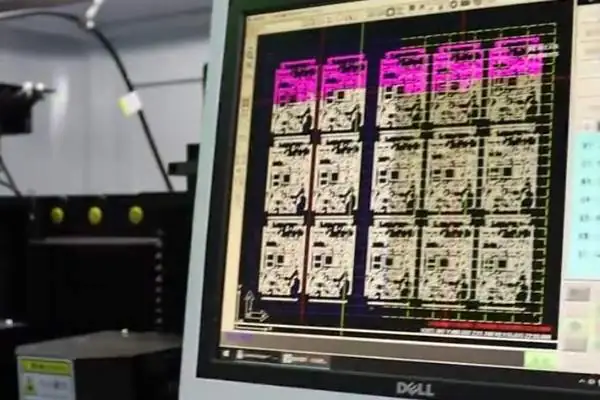
I once visited an automated workshop and saw them using infrared monitoring to adjust the baking temperature in real time. This is true intelligent manufacturing—not just stacking robots, but making the data flow.
Ultimately, a suitable production plan is not simply a matter of applying standard processes. The product’s application scenario must be considered. Industrial control boards and consumer electronics have vastly different reliability requirements. Blindly pursuing high-end processes will only increase unnecessary costs.
Recently, I helped a medical device company revamp their production line. They had previously copied the immersion gold process from the telecommunications industry, but it was not suitable for medical circulatory systems.
In practical applications, the differences are often negligible, as reliability and cost control are the eternal themes of manufacturing.
I’ve seen many people focus on sophisticated design software when discussing PCB manufacturing. However, the key factors determining whether a board works often lie in the most inconspicuous details – for example, the seemingly simple drilling process.
Many people think drilling is just making a hole. But consider what happens if the hole walls aren’t properly treated? I once encountered a prototype board with a perfect design that consistently had unstable signals. Later, we discovered that burrs left after drilling were causing unreliable connections. This made me realize that the most easily overlooked details in Production de circuits imprimés are often the most critical.
Let’s talk about electroplating. Some manufacturers simplify the process to save costs, resulting in uneven copper plating thickness inside the holes. You might think a few micrometers don’t matter, but high-frequency signals are particularly sensitive to impedance matching; variations in thickness affect performance. I’ve seen extreme cases where voids appeared in the hole walls, directly leading to the entire batch of boards being scrapped.
Regarding circuit fabrication, everyone now strives for smaller line widths and spacing, but don’t forget that the connection between the traces and the holes is the real test. Once, a high-speed board we made tested perfectly in the lab, but during mass production, we frequently encountered open circuits. We later discovered that the dry film at the edge of the holes wasn’t properly adhered during pattern transfer, allowing the plating solution to seep in and corrode the copper that should have been preserved.
The solder mask, although seemingly just a layer of green paint, has a thickness and adhesion that affect soldering yield. I handled a batch of boards where the solder mask was too thick, causing the actual ball spacing during BGA soldering to decrease, resulting in bridging problems.
These experiences have made me realize that making PCBs is like woodworking; anyone can do the surface work, but the true skill lies in the treatment of the joints. Now, whenever I see advertisements emphasizing only the number of layers and high density, I want to remind them to first master the basic processes, because even the most complex designs ultimately rely on these fundamental manufacturing steps to achieve their value.
In the field of industrial automation, people often pay attention to AI
Ever wonder how your phone maintains a stable signal? It relies on
When selecting components for a security monitoring system, most attention goes to
- Expert en production de petites et moyennes séries
- Fabrication de circuits imprimés de haute précision et assemblage automatisé
- Partenaire fiable pour les projets électroniques OEM/ODM
Heures d'ouverture : (Lun-Sam) De 9:00 à 18:30