
Industrial Automation PCB Reliability: How to Achieve 10+ Years of Stable Operation
In the field of industrial automation, people often pay attention to AI
I’ve always found those circuit boards that can be bent and folded particularly interesting. They aren’t as rigid as traditional boards. I remember once disassembling an old flip phone to study the ribbon cables inside and wondering how it could be so durable. Later, I gradually understood that this is the charm of flexible circuits. These flexible circuits typically use polyimide or polyester film as the substrate, with a thickness as thin as 0.1 mm. Combined with highly ductile electrolytic copper foil conductors, they can achieve a dynamic bending life of over 10,000 cycles. In terms of manufacturing, precision circuits are etched onto the flexible substrate using photolithography, and then a protective layer is applied to form a three-layer sandwich structure. This design ensures both conductivity and insulation safety.
Many electronic products today strive for thinness and miniaturization, making internal space extremely precious. Traditional rigid circuit boards become cumbersome. Take, for example, the camera module in a mobile phone. Connecting such a small lens and high-definition sensor to the motherboard using ordinary wiring is simply impossible. Flexible PCBs, however, can easily weave through narrow gaps like ribbons, solving wiring problems and allowing for more flexible designs. For instance, the periscope telephoto lens commonly found in full-screen phones uses multi-layered flexible circuits to achieve signal transmission between the optical components and the motherboard. Its Z-shaped folding design is only 1.5 mm at its thinnest point, a structure completely impossible for rigid circuits. In the wearable device field, smartwatches extensively utilize curved, flexible circuitry within their curved crowns, allowing electronic components to perfectly conform to the curves of the human wrist.
The automotive industry’s demand for this technology is also evident. Modern cars are filled with various sensors and displays, their wiring resembling a spider web. Ordinary wiring harnesses are thick, stiff, cumbersome to install, and prone to failure. However, flexible connection solutions simplify everything, allowing wiring to follow the contours of the car body, saving space and improving reliability. For example, in the adjustment system of car power seats, using flexible circuitry instead of traditional wiring harnesses reduces weight by approximately 40% and allows for synchronized movement with the seat tracks without wear. In smart cockpit scenarios, curved displays spanning the center console rely on transparent flexible circuitry to achieve seamless display. This circuitry is made using indium tin oxide conductive material on a PET substrate, maintaining both light transmittance and conductivity.
Some flexible PCB manufacturers I’ve spoken with have mentioned that their products are no longer just simple connectors; some even integrate basic components directly onto flexible substrates to form a complete functional system. This integrated approach is truly impressive. For example, recently developed flexible sensing systems embed pressure sensors, temperature detection units, and Bluetooth communication modules onto a single elastic substrate, allowing them to be directly attached to sportswear to monitor athletes’ physiological data. Further cutting-edge research is exploring printing micro fuel cells on flexible substrates, generating electricity from lactic acid molecules in sweat to power wearable devices.
The reliance on this technology in the medical device field is self-evident. Portable monitoring devices and imaging units in endoscopes require extremely flexible and reliable circuitry. After all, these devices either come into direct contact with the human body or operate within narrow cavities; any stiffness could affect their effectiveness. Currently, the most advanced electronic skin patches can achieve ultra-thin circuits with a thickness of only 50 micrometers, with an elastic modulus similar to human dermal tissue, and do not cause skin allergies even after 72 hours of wear. In neurosurgery, flexible electrode arrays can be wrapped around the surface of the cerebral cortex to precisely monitor neuronal activity, with a bending radius of less than 0.5 millimeters, making them far more adaptable to the irregular curvature of biological tissues than traditional electrodes.
While flexible technology sounds sophisticated, practical applications still face various challenges, such as durability after repeated bending and stability in high-temperature and high-humidity environments. These require continuous improvement in materials and processes. However, judging from the current development momentum, the potential of this technology is far from being fully explored, and many more unexpected applications are sure to emerge in the future. Research institutions are developing self-healing elastic conductors; when microcracks appear in the circuit, embedded microcapsules release conductive polymers to repair them. In extreme environment applications, polytetrafluoroethylene (PTFE) flexible circuits can withstand temperatures of 200°C and 95% humidity, providing new solutions for the aerospace field.
Sometimes, looking at these freely bendable circuit boards in my hands, I can’t help but marvel at the incredible advancements in technology. Decades ago, who could have imagined that rigid circuits could become as soft as fabric? Now, laboratories have developed washable textile circuits, weaving silver nanowires into cotton fibers. The resulting smart clothing retains its functionality even after 50 machine washes. Even more astonishing is the progress in bionics. Scientists have designed a flexible mesh circuit that mimics the vascular structure of insect wings, capable of completely recovering its original shape after being stretched and deformed by 300%. This smart material represents a revolutionary breakthrough for soft robotics.
Recently, while researching the internal structure of electronic devices, I discovered an interesting phenomenon—the seemingly insignificant connections often determine the lifespan of the entire product. For example, the repeatedly folded parts of a phone or the wiring in a smartwatch strap use special circuit boards that can bend easily.
Traditional rigid circuit boards are like a thin biscuit, easily broken with slight force. Good flexible circuits, on the other hand, should be like a yoga instructor’s wrist, able to rotate 360 degrees while maintaining stable current conduction.
I remember disassembling an old flip phone; the gold wires at the flip opening remained intact after tens of thousands of bends. This durability depends not only on the material itself but also on the ingenuity of the connection design.
Many manufacturers now like to boast about the number of layers in their composite structures, but my experience tells me that sometimes a simple, single-layer design is more reliable.
During a factory visit, I noticed a detail: when handling the transition between rigid and flexible parts, workers meticulously wrapped the edges of different materials, much like making sushi rolls.
The craftsmanship of this transition area directly impacts the equipment’s impact resistance.
Speaking of heat dissipation, I discovered that some high-end devices embed micro-metal sheets in flexible areas, allowing for rapid heat conduction without hindering bending.
This design approach is ingenious—it’s not simply about piling up materials, but about allowing each material to leverage its strengths. It’s like mixing different yarns when knitting a sweater, maintaining elasticity while enhancing warmth.
When choosing suppliers, I value their sample test reports. Some manufacturers provide resistance change curves after 100,000 bends; this data is more convincing than exaggerated advertising.
Many smart wearable devices now weave circuitry directly into the fabric, an innovation reminiscent of ancient armor-making techniques—weaving metal wires into the fabric for protection.
Modern technology sometimes needs to learn from traditional craftsmanship.
Truly excellent flexible circuit design should resemble the ligaments of human joints, possessing both sufficient range of motion and maintaining connection strength.
Next time you see a foldable device, consider that behind those smooth opening and closing movements lies a precise art of collaboration within millimeter-level space.
I’ve always felt that many people’s understanding of flexible circuit boards remains superficial. Those winding lines are certainly cool! But what truly fascinates me is the near-perfect balance behind these paper-thin devices.
I remember once visiting a flexible PCB manufacturer’s lab and being particularly impressed by their testing—a thin film covered in circuitry was folded thousands of times and still functioned normally! I thought to myself, this thing is much stronger than our mobile phone screens.
In fact, the choice of material combination depends entirely on the desired effect. For example, the thickness of the copper foil is crucial; too thin and it’s prone to breakage, too thick and it affects flexibility. Finding the right balance requires repeated adjustments.
I’ve seen some engineers pursue ultimate flexibility while neglecting practical application scenarios, which is a misconception. Flexible circuit boards (PCBs) aren’t necessarily better the softer they are; the key is to match the final product’s usage requirements.
Some manufacturers are now promoting adhesive-free PCBs, which do perform better in high-temperature resistance, but the cost has also increased significantly. Whether or not to spend this extra money depends on the specific project budget and performance requirements; it’s not a one-size-fits-all answer.
There’s a detail many people might overlook—those seemingly simple adhesives are actually quite complex. Different adhesive formulations have significant differences in aging resistance; choosing the wrong one can lead to delamination issues within a few years.
Recently, while designing a wearable device for a friend, I discovered an interesting phenomenon: the performance of flexible printed circuit boards of the same specifications varied much more significantly under different temperature and humidity environments than expected. This reminds us that we must consider the usage environment when planning products.
Frankly, many emerging fields are bringing new challenges to flexible circuits. For example, foldable screen phones need to withstand hundreds of thousands of bends, which places higher demands on material durability. Traditional approaches may need to be re-examined.
Sometimes I feel like working in this industry is like playing a balancing act, finding the perfect equilibrium between flexibility and reliability—a process that’s both grueling and incredibly rewarding.
Have you noticed that the failure rate of flexible electronic products has actually decreased significantly in recent years compared to earlier years? This is largely due to overall advancements in materials science and technology, especially the upgrades in copper foil processing technology.
What I admire most are the flexible PCB manufacturers who pay attention to detail. They don’t cut corners to reduce costs; for example, they maintain high standards even in unseen areas like the uniformity of adhesive coating.
Ultimately, a good flexible circuit design should be like a tailor-made garment for an electronic product—not too tight to restrict movement, and not too loose to compromise protection. Finding this perfect balance requires years of experience.
Seeing more and more products using flexible circuits makes me wonder: are flexible solutions suitable for all situations? Sometimes, traditional rigid boards might be a more economical and practical choice.
Recently, I experimented with combining substrates of different thicknesses and unexpectedly discovered that certain combinations can simultaneously improve flexibility and mechanical strength. This made me realize once again that materials science is always full of surprises.
In which field do you think the biggest breakthrough in flexible circuits will occur in the next decade? I guess it might be in biomedicine, since the human body’s requirements for device comfort are far more stringent than in any other scenario.
I’ve always found circuits that can bend and flex incredibly interesting. We used to think electronic devices should be square boards crammed into boxes, until the advent of flexible PCBs shattered this stereotype. These flexible circuits have brought completely different possibilities to product design.
I remember seeing a fitness tracker once that used flexible circuit board technology; the entire device could naturally conform to the curve of the wrist. This made me realize that when circuits are no longer limited by rigidity, electronic products can better adapt to the shape of the human body. Traditional rigid boards always feel cold and inflexible, while flexible design makes technological products more approachable.
Many electronic products are now pursuing thinner and lighter forms, which is inseparable from the contributions of flexible circuits. A project I recently worked on used a rigid-flex design approach, retaining the stability of traditional PCBs while incorporating the flexibility of flexible connections. This design allows for better utilization of the product’s internal space.
Choosing a reliable flexible PCB manufacturer is indeed crucial. I’ve seen cases where manufacturers’ insufficient understanding of material properties led to product problems in actual use. Flexible circuits place higher demands on materials and processes than traditional circuits.
In fact, the significance of flexible technology goes far beyond simply making devices thinner and lighter. It allows electronic products to better integrate into our daily lives. For example, wearable devices need to bend with human movement, and medical devices need to adapt to the human body’s contours; both require flexible circuitry.
In the future, we will see even more innovative applications. Imagine electronic devices that can be folded at will or sensors that can be used like stickers—all of these rely on flexible circuit technology.
I think the most important thing is to understand that the essence of flexibility is not about showing off technology but about solving problems. When designers truly start from the user’s needs, flexible circuits can realize their greatest value.
I recently talked to a friend who works in wearable devices about a problem they encountered—the circuit boards that bend and fold always fail in critical areas. He mentioned that a flexible PCB manufacturer supplied them with components that experienced circuit breakage during folding tests.
This reminds me of a scene I witnessed at a factory I visited before—workers were using laser equipment to precisely process the cover layer.
What many people easily overlook is that the real challenge of flexible circuit boards often lies not in the materials themselves, but in the precision required for the fit between the various components.
Take opening windows in the cover layer, for example. Traditional stamping methods are indeed efficient, but they fall short when faced with complex designs.
I once saw technicians repeatedly adjusting alignment parameters while debugging equipment, just for a few micrometers of error. They told me that sometimes a batch of defective products is due to a deviation in this step.
Many manufacturers are now using ultraviolet laser cutting to handle these delicate tasks, which does achieve more precise control, but it also places higher demands on the operators’ skills.
The most precise flexible circuit boards I’ve seen have linewidths as thin as a human hair, but products with this level of precision require extreme care during assembly; even the slightest misalignment can lead to functional failure.
I remember a medical device company whose products underwent tens of thousands of bending tests, only to discover that the root cause of the problem was uneven adhesion between the cover layer and the substrate.
Speaking of this, I feel that many manufacturers are currently focusing too much on breakthroughs in individual processes while neglecting the importance of overall coordination. It’s like a jigsaw puzzle; every piece must fit perfectly to ensure the final result.
Once, I saw engineers spend two whole days debugging new equipment, optimizing the collaboration between the laser cutting and alignment systems. They said this directly affects the yield rate.
From the user’s perspective, we are more concerned with whether these precision manufacturing processes ultimately deliver a reliable user experience. After all, nobody wants their smartwatch to develop display problems after only six months.
Recently, I heard that some manufacturers are starting to try new lamination technologies, which supposedly offer better control over the alignment accuracy between the cover layer and the circuitry. This is a direction worth paying attention to.
Ultimately, manufacturing flexible circuit boards is like dancing in a microscopic world; every movement must be precise to produce a perfect performance.
I’ve seen too many people make the same mistake when designing flexible circuits—treating flexible PCBs as mere substitutes for ordinary circuit boards. The most fascinating aspect of this technology is precisely its bendable nature.
I remember once helping a friend revise a design for a smart bracelet. They initially laid out the flexible circuit board like ordinary circuitry, completely ignoring the stress distribution during wrist movement. As a result, the sample broke after less than a thousand bends.
Truly excellent flexible PCB manufacturers understand one thing: these paper-thin lines are alive. They need to breathe and move.
Have you ever seen a leaf fall? It doesn’t fall straight down but swirls and drifts with the airflow. Flexible printed circuit board design should also have this sense of fluidity.
I particularly enjoy observing the parts of electronic products that bend repeatedly, such as the hinge of a flip phone or the hinge area of a foldable screen. You’ll find that experienced engineers always make special adjustments in these areas—widening the conductors into a teardrop shape or using symmetrical structures to balance stress.
Once, while disassembling a brand of true wireless earbuds, I discovered a clever wavy trace on their flexible circuit board where the charging contacts were located. This prevented the slight pressure from the earbuds being directly transmitted to the solder joints when placed in the charging case.
Many people think that choosing flexible materials solves everything, but understanding the actual movement trajectory of the product during use is even more important.
I often tell my team that when designing flexible circuits, they should imagine themselves as that copper foil conductor. Where would you feel the most discomfort when bent? Which corners would accumulate pressure? This kind of empathy often reveals problems that are not visible on the schematics.
Many smart wearable devices now weave circuitry directly into the fabric, presenting new challenges for flexible PCBs. Traditional straight traces are more prone to problems here, requiring adjustments to the trace routing based on the fabric’s stretching and contraction characteristics.
Sometimes the simplest solutions are the most effective, such as reducing copper density in frequently bent areas or providing sufficient buffer curvature for the conductors. These seemingly insignificant details can double the product’s lifespan.
Ultimately, the essence of flexible circuit design lies not in pursuing the ultimate bending radius, but in finding the optimal balance between mechanics and electricity. This requires designers to understand both material properties and practical application scenarios.
Next time you face a circuit board that needs to be bent, try holding it and folding it several times to feel the material’s toughness and limits. This is more intuitive than any simulation software.
I’ve always felt that many people have a misunderstanding of flexible circuit boards. Those paper-thin boards are truly tested not by the material’s flexibility, but by its durability. I remember a project last year that used a product from a flexible PCB manufacturer, and it broke during testing. Later, we discovered the problem was with the copper foil treatment—ordinary electrolytic copper foil simply cannot withstand repeated bending.
Currently, PI (polyimide) is indeed a good choice among common flexible substrates on the market. Its heat resistance is excellent, but the price is indeed hesitant. Sometimes I wonder if all applications need to use such high-specification materials? For example, for products that only require a simple bend once, ordinary polyester materials might be more economical.
I’ve seen many engineers blindly pursue thickness parameters, insisting on specifying a certain mil value for the material, resulting in doubled costs. In fact, many consumer electronics applications don’t require such precise specifications.
The liquid crystal polymer material I recently encountered has really impressed me. This new material exhibits superior stability under varying humidity levels compared to traditional PI, making it particularly suitable for environments with large temperature differences.
When choosing flexible circuit boards (FPCBs), the simplest aspect is often overlooked – the bending radius design. Some engineers, in pursuit of thinness, design the bending radius too small, which can cause problems even with the best materials. It’s like folding a piece of paper too many times – it will always leave creases.
In fact, choosing materials for FPCBs is like choosing shoes; a good fit is more important than aesthetics. There’s no need to prioritize specifications at the expense of practical application scenarios – that’s the most practical consideration.
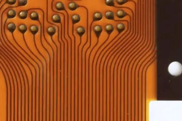
I recently disassembled an old phone to examine its internal structure. The most captivating thing when I opened the back cover wasn’t the motherboard chip, but rather the easily bendable connecting wires resembling black tape. These are what people commonly call FPC circuitry. They flexibly connect components like the screen and camera. A close examination of the cross-sections of these FPCs reveals a multi-layered structure, with the thinnest part only 0.1 millimeters thick. The middle layer is copper foil circuitry, wrapped in an outer polyimide film. This material maintains its flexibility in extreme temperature environments ranging from -40°C to 125°C, which is the key to its ability to replace traditional wiring harnesses.
I used to think that circuit boards should be rigid, green boards. It wasn’t until I got involved in wearable device design that I realized rigid PCBs can be a burden in many situations. I remember once working on a smart bracelet project. The engineers insisted on using traditional circuit boards. The resulting product was always uncomfortable on the wrist. Later, we switched to a flexible circuit design. The whole experience was completely different. The new design uses a wavy wiring layout, allowing the circuitry to expand and contract like an accordion bellows when the wristband bends, effectively distributing stress. We also added reinforcing ribs at key points to prevent copper foil breakage caused by repeated bending.
Choosing a reliable supplier is indeed a technical skill. We once collaborated with a factory that claimed to be able to do special bending designs. The samples looked good. However, during mass production, the circuits broke. Later, we realized that the substrate they used didn’t meet fatigue resistance standards. Reputable manufacturers use rolled copper instead of electrolytic copper as the conductive layer. The former has a more uniform grain structure and has been tested to withstand over 100,000 dynamic bends. Inferior materials often show impedance changes after only 5,000 tests.
Many innovative products now utilize this characteristic. For example, the snake-like structure of an endoscope camera conceals a spirally arranged flexible PCB. This ensures signal transmission while allowing 360-degree rotation. This design uses biomimicry principles, mimicking the movement of the human spine, with each PCB segment bridged by elastic connectors, ensuring signal integrity while enabling multi-degree-of-freedom movement.
However, it’s important to note that this design is not a panacea. For areas requiring frequent bending, the bending radius must be controlled. For static installations, using ordinary FR4 board is more economical and reliable. For example, for fixed-installation components like appliance control panels, using rigid PCBs may cost only one-third of a flexible solution and is easier to automate soldering production.
I was particularly inspired during a visit to an automotive electronics exhibition. I saw a rigid-flex PCB with a three-dimensional structure replacing more than twenty wire harnesses in a car door module. This three-dimensional wiring approach completely changed my understanding. They integrated the wiring connecting the window regulators and door lock sensors into a tree-like structure. The rigid board carries the power devices, while the flexible board extends to the actuators like nerve endings, reducing the module weight by 40%.
Ultimately, technology is just a tool. What’s truly important is understanding the dynamic characteristics the product needs. Take smart insoles as an example: we tested three wiring schemes: straight lines tend to cause stress concentration at the arch, grid lines affect the insole’s elasticity, and finally, radial wiring perfectly matched the foot’s movement trajectory.
I recently gained a deep understanding of this while helping a friend upgrade their drone’s image transmission system. Originally, a ribbon cable was used to connect the flight controller and camera. Signal interference always occurred during periods of high vibration. Later, we switched to a twisted-pair flexible circuit and added silicone cushioning pads at the connectors, improving the signal-to-noise ratio by 15dB under high-frequency vibration. This seemingly small improvement resulted in a qualitative leap in the stability of aerial footage.
In fact, the applications of this type of material are more widespread than imagined. In the medical field, the shell of a swallowable capsule endoscope contains a spiral FPC (Flexible Printed Circuit). This FPC must deform with intestinal peristalsis while ensuring a stable power supply to the miniature camera. Designers even considered the corrosiveness of digestive tract fluids, adding a medical-grade polyurethane coating to the protective layer.
Last month, while repairing an old film camera, a similar elastic contact plate was discovered in the shutter curtain. These designs from the 1970s already showcased the rudiments of flexible electronics. The steel plate completes the circuit switching with each shutter click, requiring a lifespan of over 100,000 cycles. This demonstrates that excellent mechanical design and material processing are always complementary.
Ultimately, good design should make the technology imperceptible. Like the multi-layered FPC in the hinge of a foldable screen, you’ll only marvel at the smooth opening and closing of the screen, but you won’t imagine that it hides seventeen layers of precision circuitry capable of withstanding 200,000 bends. These circuits use a staggered, stacked design, with each layer’s bending axis precisely calculated, like dressing electronic components in ballet shoes, allowing technology to perform an elegant dance within a small space.
This is perhaps the highest realm of engineering art—transforming the most complex technology into the most natural experience. When users can enjoy the pleasure of seamless folding without understanding the millimeter-precision hinge structure, and when patients can obtain accurate diagnoses without knowing the nanoscale coating technology, this seamless integration of technologies is the true meaning of innovative breakthrough.
In the field of industrial automation, people often pay attention to AI
Ever wonder how your phone maintains a stable signal? It relies on
When selecting components for a security monitoring system, most attention goes to
- Expert en production de petites et moyennes séries
- Fabrication de circuits imprimés de haute précision et assemblage automatisé
- Partenaire fiable pour les projets électroniques OEM/ODM
Heures d'ouverture : (Lun-Sam) De 9:00 à 18:30