
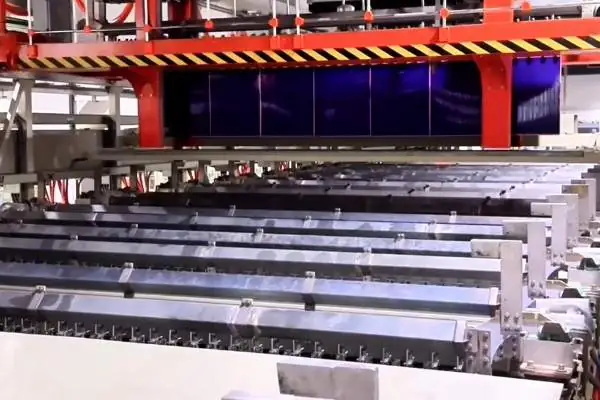
Heat Dissipation Challenges and Solutions in PCB Circuit Board Design
Circuit boards are more than just that green board in a phone
I’ve recently been thinking about something – why have Teflon PCBs become almost irreplaceable in certain specific fields? This stuff is really quite interesting.
What you might not know is that Teflon is actually a general term for a large family of materials, and PTFE is just one of its most famous members. A common characteristic of this series of materials is that they naturally don’t like to interact with other substances; their surface energy is incredibly low, and almost nothing sticks to them. This characteristic makes them particularly popular in high-frequency circuits because signal loss can be minimized.
I remember once helping a friend debug a millimeter-wave radar module that used a ceramic-filled Teflon board. My most immediate impression was that this material was indeed much more difficult to process than ordinary FR4, but the performance stability was on a completely different level. Especially in scenarios with drastic temperature changes, ordinary boards are prone to deformation, leading to impedance drift, while the Teflon series has excellent control over its thermal expansion coefficient.
However, this material isn’t a magic bullet. Its mechanical strength is relatively weak; using pure PTFE for rigid circuit boards can even cause problems with drilling. Therefore, the commonly available Teflon PCBs on the market are basically composite forms – either mixed with glass fiber cloth to enhance hardness or mixed with ceramic powder to adjust the dielectric constant.
The most ingenious application I’ve seen is in satellite communication equipment, where different Teflon materials with varying dielectric constants are used to create a multilayer structure, ensuring both signal integrity and miniaturization. This approach requires designers to have a particularly deep understanding of material properties, as the processing techniques for PTFE series materials are completely different from traditional epoxy resins.
Now, some manufacturers are starting to introduce modified Teflon materials that retain the low-loss advantages while improving drilling performance and bonding strength. This is a good direction, because even the best electrical characteristics are useless if the material can’t be made into a product.
Ultimately, choosing whether or not to use Teflon PCBs is like choosing running shoes – it depends on the specific application. If you’re running a marathon, you’d choose lightweight shoes with good rebound; if you’re hiking, you’d choose shoes that are non-slip and wear-resistant. High-frequency circuit design is the same; the key is to clearly understand what problem you’re trying to solve.
When I was working with high-frequency circuit boards, I noticed a rather interesting phenomenon – many people think of Teflon PCBs as a panacea. In reality, material properties are just the foundation; what truly determines performance are those seemingly insignificant design details.
I remember once debugging a millimeter-wave module; even though we were using a top-of-the-line Teflon substrate, the signal quality just wasn’t good enough. Later, we discovered the problem was in the via design. To save space, the vias were placed very close together, resulting in much more severe impedance discontinuities than expected. This discontinuity might not be noticeable at low frequencies, but it becomes a fatal flaw at high frequencies.
Speaking of impedance control, I actually think microstrip line structures aren’t as mysterious as some people make them out to be. Some people get too caught up in the calculation formulas, but in reality, on-site adjustments rely more on experience. For example, although the Dk value of the board material is nominally stable, there will be slight variations after processing. In this case, stubbornly sticking to theoretical values is less effective than leaving some room for adjustment. I once solved a standing wave ratio problem in an antenna feed line by fine-tuning the line width, which was much more effective than simply changing the material.
Ground-plane coplanar waveguides are actually underestimated. Their advantage isn’t in their theoretical perfection, but in their higher tolerance for manufacturing errors. Especially when the board thickness is slightly uneven, traditional microstrip lines can experience impedance variations of more than 10%, while coplanar structures can maintain relative stability.
What surprised me most was how many people mishandled right-angle corners on Teflon boards. Many simply copied the FR4 approach and suffered significant consequences. Because of the unique dielectric properties of Teflon, the phase distortion caused by right angles is more pronounced than with ordinary board materials. We only completely solved the problem by using rounded corners. These details are impossible to discover just by looking at the datasheet.
Now, when I see those advertisements that hype up Teflon PCBs, I feel they’re a bit one-sided. Even the best materials need to be combined with a reasonable design. Sometimes, a different approach is more useful than simply using more expensive materials, don’t you think?
Every time I see someone discussing high-frequency circuit boards, I’m reminded of my first experience with Teflon PCBs. Back then, the senior technician in the lab handed me a board and mysteriously said, “This stuff is very precious.” I was puzzled at the time; it was just a green circuit board.
Later, I understood the special characteristics of Teflon PCBs: their stability. Ordinary FR materials are prone to deformation with temperature changes, just like a plastic ruler bends when heated. But the ceramic filler added to the Teflon substrate makes it exceptionally stable, which is especially noticeable in environments with large temperature fluctuations. I remember once doing outdoor equipment testing, and the circuit parameters of ordinary boards fluctuated significantly.
Speaking of PTFE materials, what surprised me most was its dielectric properties. In a comparative experiment, I found that the signal loss of Teflon boards at the same frequency was significantly lower than that of conventional materials. This reminded me of how I used to have to add various compensation circuits when using ordinary boards.
Many people think that Teflon PCBs are difficult to process, but the technology has improved a lot now. However, the issue of thermal expansion coefficient does need attention.
I’ve seen people blindly using Teflon boards in pursuit of low loss.
I recently encountered this situation while helping a friend modify a drone video transmission project.
Actually, material selection is like choosing shoes.
Some manufacturers are now packaging hydrocarbon materials as high-end alternatives.
Ultimately, the key to using Teflon PCBs effectively lies in understanding their characteristics.
I remember once during debugging a millimeter-wave module, I discovered an interesting phenomenon: the performance of the same design on different board materials varied much more than expected.
This experience made me realize how interesting hardware design is – the choice of materials can often lead to unexpected results.
However, the price of Teflon PCBs has indeed come down now, unlike ten years ago when they were prohibitively expensive. This is good news for those of us who love tinkering; we can experiment with various design ideas more freely.
I’ve always felt that Teflon PCBs have been overly glorified. Yes, their high-frequency performance is excellent, but what truly determines the success or failure of a project are the most fundamental aspects. I remember when we first started working with this type of material, everyone on the team was fixated on parameters like the dielectric constant. As a result, the first batch of boards was completely scrapped due to material compatibility issues.
The feel of Teflon material is completely different from ordinary FR4; you can feel its unique flexibility just by holding it. However, this material has incredibly demanding processing requirements. Once, we discovered that seemingly perfect boards developed microcracks during vibration testing. We later realized this was due to the difference in thermal expansion coefficients between the substrate and the copper foil—a problem that wouldn’t be detected in conventional testing.
Now, when validating Teflon PCBs, we pay special attention to three dimensions: high-frequency performance is just the entry point; more importantly are long-term environmental adaptability and mechanical stability. The boards we made for a space project underwent three months of alternating humid and dry heat testing—cyclic shock from -60 degrees Celsius to +150 degrees Celsius. This extreme validation is necessary to expose the material’s true weaknesses.
Interestingly, the advantages of Teflon material can sometimes be a double-edged sword. Its low-loss characteristics do ensure signal integrity, but it also means zero tolerance for surface contamination. Once, a customer complained about abnormal signal attenuation, and after a long investigation, we found that someone in the assembly workshop had been wearing gloves containing silicone oil. This kind of detail wouldn’t cause any problems with ordinary PCBs, but it became a fatal issue with Teflon.
I now tend to view Teflon PCBs as precision instruments rather than ordinary circuit boards. They require a high degree of coordination across design, manufacturing, and testing. For example, when performing impedance testing, the impact of probe pressure on the soft substrate must be considered; these subtle operational differences can lead to completely different measurement results.
What truly changed my perspective was the millimeter-wave radar project we worked on last year. We initially thought that using good materials would guarantee performance, but we found that phase consistency completely depended on the uniformity of the board material. Sampling and testing the same batch of Teflon substrate at different locations showed dielectric constant variations as large as 0.02. This lesson taught me that even the best materials require scientific validation methods.
Now, when I see people designing based solely on parameter tables, I can’t help but want to remind them: the true value of Teflon PCBs lies not in how impressive their theoretical performance is, but in how well you can leverage their stability. This is like a racing car engine; peak horsepower is just a number on paper, but the key is whether it can consistently deliver that power on the track.
When I first started working with high-frequency circuits, I also made some mistakes. I always thought that ordinary PCB boards would be sufficient for all designs. It wasn’t until a project experienced significant signal attenuation that I realized the problem. Later, when I encountered Teflon PCBs, I understood what it means to use the right tool for the job. The most special thing about this material is its exceptionally stable dielectric properties. Signals running on it experience almost no energy loss. This difference is particularly noticeable when working with microwave circuits. Ordinary board materials suffer significant signal attenuation in high-frequency environments, while Teflon PCBs maintain the signal very well. It’s like the difference between driving on a muddy dirt road and a paved highway – both are roads, but the experience is completely different.
I remember once debugging a millimeter-wave module. I couldn’t get it to work with ordinary board material. Switching to a Teflon substrate solved the problem immediately. This experience was very intuitive. Now, when doing high-frequency designs, I always prioritize Teflon material. Specifically, when operating in the 24GHz and above frequency range, the dielectric constant of ordinary FR-4 board material fluctuates dramatically with frequency, leading to phase distortion and impedance mismatch. However, the dielectric constant of Teflon material remains almost constant at around 2.1 in the 1MHz to 40GHz range. This stability is crucial for maintaining the signal waveform.
However, this material also has its drawbacks. The processing difficulty is significantly greater than that of ordinary PCBs. The lamination process, in particular, requires very high precision. Even a slight lapse in temperature control can cause problems. Because Teflon has a melting point of approximately 327℃, but a large coefficient of thermal expansion, warping can easily occur during drilling and copper plating. Furthermore, its low surface energy requires special plasma treatment to ensure the adhesion of the copper foil. These processing challenges make the manufacturing cost 30-50% higher than that of ordinary board materials.
But having said that, these troubles are worth it. After all, the performance speaks for itself.
I now habitually use Teflon PCBs for critical signal paths. For other parts, I still use conventional materials to control costs. For example, in RF front-end design, only the antenna feed line and filter sections use Teflon substrates, while the power management and digital control circuits still use the lower-cost FR-4 material. This hybrid design ensures core RF performance while keeping overall costs within a reasonable range.
Choosing materials is like choosing tools. More expensive isn’t always better; the material needs to be suitable for the specific application. For low-frequency digital circuits, there’s no need to use Teflon.
However, when it comes to high-frequency analog signals or RF circuits, the advantages of this material become apparent. For example, in automotive radar modules, a Teflon substrate can keep the insertion loss of a 77GHz signal below 0.3dB/cm, while ordinary materials might reach over 1.2dB/cm. This difference directly determines the detection range and resolution.
Recently, while working on 5G-related projects, I’ve noticed that more and more designs are adopting Teflon substrates. This indicates that the industry’s requirements for signal integrity are becoming increasingly stringent. Previously, using ordinary board materials might have been acceptable, but that’s no longer the case. Especially in base station antenna array designs, which need to handle multiple 28GHz/39GHz frequency band signals simultaneously, demanding stringent requirements for the dielectric loss and temperature stability of the board material.
This change is quite interesting. It reflects the overall industry’s increased demand for performance.
Sometimes I think that material selection reflects an engineer’s design philosophy: whether to be satisfied with basic functionality or to pursue ultimate performance. For example, in satellite communication equipment, even a 20% increase in cost, the 0.5dB noise figure improvement brought about by using a Teflon substrate can mean a significant improvement in the reliability of the communication link.
Of course, this doesn’t mean that all projects should use the best materials. The right choice should be made based on actual needs. For example, consumer Bluetooth headphones, due to their low operating frequency and cost sensitivity, can use ordinary high-frequency board materials; blindly using Teflon would only lead to wasted resources.
After all, a good design finds the optimal balance between performance and cost.
While tinkering with high-frequency circuits in the lab recently, I noticed an interesting phenomenon—those who tout high-performance RF designs often overly rely on material parameter tables. Take Teflon PCBs, for example; many people’s eyes light up when they see the low loss coefficient, as if using this substrate automatically unlocks millimeter-wave performance.
Last week, I encountered this situation while helping a junior colleague debug his automotive radar module. He insisted on using an imported Teflon substrate, but during soldering, the mismatch in thermal expansion coefficients caused the microstrip lines to lift. In fact, at the 77GHz frequency band, ordinary FR4 performs quite well after precise impedance compensation. The key is to make trade-offs based on the actual application scenario – after all, what’s most needed in a vehicle environment is vibration resistance, not the ultimate dielectric constant.
Some manufacturers are misleadingly marketing Teflon PCBs as a universal solution. I remember visiting a communication base station factory once, and an engineer pointed to the composite dielectric board in the AAU unit and told me that they controlled the loss of ordinary materials to within 0.002 through structural innovation, while the cost was only one-sixth of that of Teflon. This pragmatic approach is much smarter than blindly using expensive materials.
The real test of skill is maintaining stable performance at a specific frequency. The most ingenious design I’ve seen was in a Ku-band satellite receiver, where a three-layer lamination technique was used to apply Teflon only to the critical resonant areas, controlling overall cost while ensuring phase consistency. This precise approach is far more skillful than using high-end materials throughout.
With the development of terahertz technology, simply pursuing low-loss materials may lead to a dead end. Last year at an industry exhibition, I saw an interesting solution: through electromagnetic field reconstruction technology, ordinary fiberglass boards performed better than some special substrates at 140GHz. This reminds us to consider – when the wavelength is shortened to the micron level, perhaps surface treatment processes are more important than the substrate itself.
Ultimately, choosing PCB materials is like choosing clothes; there is no single best option. The important thing is to understand what your circuit truly needs, rather than being led astray by marketing jargon. The next time you design a high-frequency board, you might want to calibrate your oscilloscope first, after all, actual measurement data is always more convincing than parameter tables.
I’ve always felt that Teflon PCBs are overrated in RF design. Many people immediately turn to Teflon when discussing high-frequency applications, as if using it automatically elevates performance to a higher level. While Teflon materials do have their advantages, such as low loss characteristics which are highly valued in antenna design, this doesn’t mean it’s a universal solution. I’ve seen many designs where, in pursuit of theoretically perfect specifications, designers insisted on using Teflon substrates, doubling the project cost, only to find that a standard FR4 board with some optimization could have met the requirements.
I remember once debugging a millimeter-wave antenna array, where the team insisted on using a Teflon PCB for the feed network. However, during repeated impedance matching adjustments in the lab, they found that the overly stable dielectric constant became a problem, as tiny deformations in the surrounding structural components amplified phase deviations. Later, switching to a composite dielectric board made it easier to flatten the phase response. This made me realize that material selection shouldn’t just be based on datasheets but should consider the actual application scenario.
Teflon surface treatment is indeed a headache, but now plasma activation technology is much more reliable than traditional chemical treatment, at least avoiding blistering of the copper foil after lamination. But honestly, these process difficulties deter many small manufacturers, leading to processing times of four weeks or more for Teflon PCBs. This time cost is simply not friendly for prototype designs that require rapid iteration.
I prefer to view Teflon PCBs as specialized tools rather than standard options. For example, in scenarios like satellite communication terminals, where loss is extremely critical, its value truly shines. However, 5G antennas in ordinary consumer electronics can now be handled with modified epoxy resins or even liquid crystal polymers. After all, engineering design is essentially about finding a balance under various constraints, not pursuing the optimization of a single indicator.
Recently, I helped a friend modify a drone image transmission module. The original design used a Teflon microstrip antenna, but later we found that switching to a ceramic-filled PTFE composite material resulted in greater stability in vibrating environments. This reminded me of an interesting phenomenon: many people are fixated on the purist approach to Teflon, neglecting the fact that many improved high-frequency materials are equally effective, some even exhibiting superior temperature stability.
Ultimately, choosing a PCB material is like choosing a camera lens – there’s no such thing as the best, only the most suitable. I’ve seen too many cases where blindly pursuing high-end materials complicates simple problems. What’s truly important is understanding the behavior of electromagnetic waves in the dielectric medium, not being misled by material marketing. After all, even the best Teflon PCB can’t save a poorly designed feed network. While recently studying high-frequency circuit design, I discovered an interesting phenomenon – many people only think of traditional materials when discussing high-performance PCBs. However, there’s an often-underestimated option in high-frequency applications: Teflon PCBs.
I remember last year, while helping a friend debug a millimeter-wave radar module, we encountered a signal attenuation problem. We tried various conventional solutions without success, but eventually solved the problem by switching to a Teflon substrate. Specifically, at the 77GHz frequency band, the insertion loss of traditional FR-4 material was as high as 3.2 dB/inch, while the Teflon substrate was only 0.5 dB/inch. This difference directly determined the radar’s detection range and accuracy. Through comparative testing with a vector network analyzer, we found that the phase consistency of Teflon boards was also improved by about 40% compared to ordinary materials, which is crucial for phased array systems.
The advantage of this material lies in its exceptional suitability for high-frequency signals. Ordinary PCBs experience a sharp increase in loss as the frequency increases, while Teflon maintains stable performance. This is because Teflon’s dielectric constant (Dk) remains stable at around 2.1 with minimal variation across frequencies, and its loss tangent (Df) is as low as 0.0009. This means that electromagnetic waves propagating through the material experience almost no molecular polarization heat loss, making it particularly suitable for high-speed digital circuits and microwave circuits that require precise phase control. For example, on a 28GHz 5G base station antenna board, a Teflon substrate can keep signal delay fluctuations within 0.1 ps/inch.
Many engineers currently misunderstand Teflon PCBs, believing them to be expensive and difficult to process. While early processing challenges were significant, domestic suppliers’ technology has matured considerably. For example, Shennan Circuits’ developed modified polytetrafluoroethylene composite material has achieved drilling accuracy of ±25μm and lamination tolerance control within ±3%. Processing costs have also decreased from 2.8 yuan per square centimeter five years ago to 0.9 yuan today, making its application in consumer-grade products such as automotive radar possible.
The most ingenious application I’ve seen is in satellite communication equipment, where designers have created a three-dimensional stack of Teflon circuits and semiconductor devices, controlling costs while ensuring performance. The specific implementation method involves laser etching microstrip lines onto a Teflon flexible substrate, then flip-chip bonding the GaAs chip onto the impedance matching circuit using conductive adhesive, and finally achieving three-dimensional integration using low-temperature co-fired ceramic (LTCC) technology. This hybrid integration architecture reduces the device volume by 60% while maintaining a voltage standing wave ratio (VSWR) of less than 1.2 in the Ku-band.
Interestingly, this material also offers possibilities for innovative designs. For example, some teams are beginning to experiment with using additive manufacturing techniques to directly fabricate specially shaped circuits on Teflon substrates, which is particularly useful in antenna design. For instance, a team at a Chinese electronics research institute used aerosol jet printing technology to directly draw a gradient slot antenna on a curved Teflon substrate, achieving broadband performance with VSWR < 1.5 in the 12-18 GHz frequency band. This non-planar circuit structure is impossible to achieve with traditional etching processes.
Of course, material selection requires balancing practical needs; not all high-frequency projects require Teflon, but for applications with extremely high signal integrity requirements, it can provide a significant improvement. For example, when a project involves QAM modulation orders higher than 1024, or symbol rates exceeding 10 Gbaud, Teflon substrates can reduce the bit error rate by one to two orders of magnitude. However, for low-frequency IoT devices, composite substrates like RO4350B might be a more economical choice.
With the development of 5G millimeter-wave and future communication technologies, I believe that these high-performance PCBs will transform from luxury items into necessities. The key is to find the right technological path for your project. Currently, the industry is exploring the integration of nano-ceramic-filled Teflon composite materials with silicon photonics chips, a technology that may solve the interconnection bottleneck in future terahertz communication. It’s also important to consider hybrid lamination techniques combining Teflon substrates with traditional materials, which can further optimize the cost structure while maintaining performance.
I recently talked to an engineer working on an RF project, and he mentioned that after using Teflon PCBs, they found delamination in several places. This is actually quite common—Teflon material itself is very stable and difficult to bond, and many people think that simply surface treatment is sufficient.
I remember last year we tried a batch of PTFE boards for experimental circuits, and we encountered problems during the etching process. At the time, we thought using standard parameters would be sufficient, but the edges of the lines turned out rough and jagged. Later, we discovered that this material is particularly sensitive to the temperature of the etching solution; a difference of just two or three degrees completely changes the result. Sometimes you think the problem is with the drilling, but the root cause lies in the material properties.
Nowadays, many people think of using Teflon PCBs when it comes to high-frequency circuits, but they often overlook the details of the manufacturing process. For example, if the drilling speed is incorrect, PTFE can easily string, resulting in rough hole walls. I once visited a factory and saw them using specially customized drill bits combined with vacuum suction to solve this problem.
Another time, something even more bizarre happened. The boards delivered by the supplier looked fine, but during testing, we found that the impedance was unstable. Upon disassembly, we discovered that the uneven flow of PTFE during inner layer lamination caused variations in dielectric thickness. This kind of problem really requires understanding the material properties, not simply blaming the manufacturing process.
In fact, the most troublesome aspect of making these boards is the coordination between different stages. For example, after surface activation, the board must immediately proceed to the next process; if left for too long, it needs to be re-processed. We learned this the hard way; a two-hour delay during lunchtime resulted in a significant drop in the adhesion of the electroless copper plating.
I think working with high-frequency boards is like conducting experiments; every time you change materials, you have to re-explore the parameters. Relying solely on standard procedures will inevitably lead to problems.
Circuit boards are more than just that green board in a phone
From disassembling old routers to visiting electronics manufacturing plants, I gradually realized
As an electronics enthusiast, I’ve come to understand firsthand the impact of
- Pienten ja keskisuurten erien tuotannon asiantuntija
- Korkean tarkkuuden piirilevyjen valmistus ja automatisoitu kokoonpano
- Luotettava kumppani OEM/ODM elektroniikkaprojekteihin
Aukioloajat: (ma-la) klo 9:00-18:30.