

SD-WAN Appliance PCB Design: Heat, Encryption Load and Signal Integrity in Fanless Edge Boxes
An SD-WAN hardware project showed how complex these boards really are: in
A PCIe Switch PCB combines dense BGA breakout, 85 ohm differential channels at 32GT/s and above, and heavy copper power and thermal planes. Few multilayer PCB manufacturers can control impedance to plus or minus 5%, handle low-loss laminates, drill backdrilled vias consistently and also process 3oz to 6oz inner copper. Success depends on separating high-speed layers from heavy copper layers in the stackup, specifying copper foil roughness and peel strength, verifying stub length and impedance with real data, and treating power integrity and thermal design as part of signal integrity.
Not long ago I took on a PCIe Switch PCB job. The board carried a 48-lane PCIe switch, mixed 4.0 and 5.0 rates on the upstream and downstream sides, and also required several stacked NVMe backplanes. The customer did not say it explicitly, but I knew the board would ultimately run at 32GT/s and might even have to push, with gritted teeth, into the tail end of 6.0 someday. The schematic was not hard; all the trouble was piled onto the PCB. After finishing the drawing, the week or more I spent looking for a factory smashed my understanding of the domestic multilayer board supply chain into pieces on the ground.
Many people think making a 20-layer board is routine now, but once copper thickness is pulled above 3oz and the stackup must be locked to high-speed material, many so-called multilayer PCB manufacturers begin to hem and haw. I asked them one by one. Some said directly that they could not control this stackup and suggested splitting the board; some did accept the order, but when I opened their engineering capability table, differential impedance could only be guaranteed to plus or minus 10%, which could not support the narrow window of 85 ohm plus or minus 5% for PCIe 5.0. In the end I gritted my teeth and found an old factory carrying the name of a high speed PCB manufacturer, and after talking I learned that in their multilayer board production line the work was actually mixed, and the lines with equipment dedicated to high-speed line cards were only a few, with scheduling so backed up it was desperate.
What could not be avoided was that HDI and thick copper fight each other. The switch board had both a large 0.5mm pitch BGA and several 60A power traces feeding GPU daughter cards, so heavy copper was necessary in the inner layers. At first I naively thought: use a 2+N+2 HDI stack, and laser drill straight down to a large copper area; is that not routine? As a result, the technician at an HDI PCB manufacturer pushed back directly: laser drilling on heavy copper layers burns unevenly, and the via wall copper thickness cannot be guaranteed. If I really wanted it, change to any-layer interconnect, at triple the price or more. Later I changed to an ordinary through-hole board, but then feared the via stub would be too long and the signal eye would close at any moment. During that time I almost harassed every HDI PCB supplier I knew, and in the end, gritting my teeth, I made the power layers separately with thick copper cores, pressed the signal layers on both sides, and locally cut away the back, stacking the whole board up to 22 layers. Cost flew to the sky, but at least the heavyweight contradiction was split apart.
Speaking of thick copper, many times heat is the craftiest enemy. A PCIe switch at full load runs around 25W, and hot air simply cannot blow through those several groups of 12V heavy copper planes inside the board. Flipping through the recommended stackups of heavy copper PCB suppliers, all of them are industrial control and automotive designs, and their heat conduction paths have never been optimized along with the signal return. Later, through a friend who makes thick copper PCBs, I found a small-scale heavy copper PCB manufacturer willing to help me insert two pieces of 6oz thick copper into the stackup as inner heat dissipation islands, and also thicken the copper in the area on the back where thermal pads are attached to 4oz, which barely brought the switching noise within specification. But then the problem came: such a thick copper PCB manufacturer usually does not touch high-speed materials, and has no experience laminating M6 or lower-loss boards, so board warpage and uneven dielectric thickness from the pressing had to be covered by myself. In the end I issued a very fussy stackup control sheet to the manufacturer, measured DK/DF on a test coupon after each lamination, and basically used their process line as a laboratory, to scrape together prototypes good enough to run.
What lies behind this actually exposes a rather awkward fact: in China, finding a multilayer PCB supplier that can handle both signals and power on a PCIe switch PCB is more tiring than sifting sand. Big factories do not want to take small and troublesome orders, and small factories often lack one leg between high speed and heavy copper. It forces hardware people like us to become half board-factory engineers, who must not only calculate insertion loss but also understand how the brown oxide chemistry affects copper foil roughness. In future, as rates rush further toward 64GT/s PAM4 with the whole link budget cut to a dozen or so dB, I truly do not know how long the existing supply chain can hold out. Perhaps within two more generations, traditional FR-4 base material and copper foil will have to yield on a large scale, and by then I fear not many HDI PCB manufacturers willing to fiddle with you will be left.
The most headache-inducing thing about designing a switch board that can run PCIe 6.0 steadily is not the rate doubling itself but that PAM4 modulation squeezes the tolerance space of the whole channel especially flat. You can hardly muddle through by reserving margin, and any inconspicuous via stub or reference plane gap that in the NRZ era might merely close the eye a tiny bit can, under PAM4, directly make link training fail. We first used an ordinary FR-4 multilayer board for the experiment, with trace length of only four or five inches, and insertion loss at the 32GHz point already soared to an unwatchable level, the eye smeared into a patch, with no hope of downstream receiving.
The problem is that many multilayer PCB suppliers on the market are used to patting their chests with their past PCIe 4.0 or even 5.0 experience, believing that piling up a few more layers and narrowing line width a bit will handle it. But at the level of 6.0, the extra attenuation brought by ordinary glass cloth and conventional copper foil roughness makes that pitiful budget evaporate instantly. Later we could only go back to find a truly high-speed-savvy high speed PCB manufacturer and iterate material selection and stackup from scratch. We finally chose a low-loss resin with ultra-smooth copper foil, and deliberately slimmed the copper thickness of the routing layers a bit, which brought channel loss within a range that could match the chip’s equalization capability. Do not underestimate the difference in copper foil roughness; at 32GHz, its swallowing of signal amplitude is far more exaggerated than many people imagine.
Switch power consumption is also an unavoidable hurdle. A PCIe Switch PCB carries over a hundred densely arranged differential pairs, and with the core chip running full 160 lanes, the heat accumulated beneath the back pad is considerable. A simple thermal via array is simply not enough; the heat forms a large gradient in the normal direction of the PCB, and local temperature rise in turn makes the dielectric Dk value drift, so the signal eye shakes with temperature. At this time, suggestions from a heavy copper PCB manufacturer become very practical: they can make four to six ounces of thick copper on outer layers and key power layers, letting the plane layers themselves become an efficient heat spreader, far more effective than attaching a heat sink externally. Of course thick copper layers and high-speed routing layers cannot be mixed casually; you must plan the large-current power layers, heat-dissipating copper and high-density signal layers in completely separate layers, otherwise skin effect and rough copper surface will give back the channel loss you worked so hard to save.
On high-density routing and interlayer transitions, the role of an HDI PCB supplier at this stage is bigger than imagined. The PCIe 6.0 channel is very sensitive to via stubs, especially when the backdrill depth is slightly off, where the remaining stub can create an obvious notch at the 30-plus GHz point. Ordinary multilayer boards going to laser holes costs too much, and the accuracy of mechanical buried and blind vias is hard to keep consistent. We found an experienced HDI PCB manufacturer who used a stacked microvia structure to compress the stub at signal layer changes to a nearly negligible level, and made the return-ground via arrangement around the differential pair on layer changes extremely symmetric. Even though manufacturing cost rose a little, it is far better than reworking after a channel failure.
In real engineering, heavy copper PCB suppliers and high speed PCB manufacturers are often two different groups: the former are good at thick copper and thermal management, and the latter have deeper understanding of low-loss materials and the impedance consistency of multilayer stacks. If you only want to save trouble and throw all requirements onto one multilayer PCB manufacturer, you will probably compromise on some subdivided performance. Our current thinking is to push the heat dissipation structure and high-speed signal routing through two stages with suppliers: the thick copper board carries current and heat dissipation, while a high-speed daughter card or core signal layers are optimized separately with low-loss board material, and finally joined through low-profile connectors or direct stacked interconnect. It looks troublesome, but in fact it breaks up the channel risk, so each segment can be verified separately for eye and bit error rate.
At the end of the day, the requirement of the PCIe 6.0 PAM4 channel on the PCB is no longer a question of whether it can be routed through; every 0.1dB of loss, every via structure and every section of copper surface roughness will leave a trace in the final system. When you discuss heat dissipation with a thick copper PCB manufacturer, you must also think about how the dielectric loss tangent changes at high temperature; when you settle the microvia structure with an HDI PCB supplier, you must also calculate whether the impedance return loss at the layer change point will eat the last few millivolts of margin of your eye diagram.
When I built switch boards in the past, for a period I was especially obsessed with controlling trace impedance to two decimal places, always thinking that as long as the simulated waveform was pretty, the board would be fine once it came back. Later, after being silenced by thermal teams in two consecutive projects, I slowly came to my senses: what really keeps one up at night on a PCIe Switch PCB is not those few pairs of differential lines but how to move away the dozens or even hundred-plus watts of power consumption from the board.
Many multilayer PCB suppliers on the market will tell you how stable their material DK is and how smooth their copper foil is, but when you ask about thick copper process and thermal channel design, you often get only the sentence we handle it with a conventional stackup. But for something like a PCIe Switch, at Gen5 and above, one chip’s power often runs seventy or eighty watts, and relying on through holes and thermal pads to conduct it is like scooping a flood with a small spoon. Later I changed to a manufacturer making heavy copper PCB and directly used 4 ounce copper on the power layers while keeping signal layers at 2 ounces, and doubled the density of the thermal via array under the chip. The measured junction temperature fell by 14 degrees, and the eye was actually more open than the prototype that used ultra-low-loss material before. This made me realize that high-speed signal integrity is very often held hostage by power integrity and thermal stability.
Another interesting thing. Many people, when looking for HDI PCB suppliers, stare at via diameter and line width and spacing. That is not wrong in itself, but do not narrow high density to fine lines. On a 16-layer PCIe Switch board I made, what I agonized over most was actually how the two thick copper power islands on the top and bottom layers would work with the microvias. Conventional HDI processes like symmetric stacked vias, but on a heavy copper layer, once a large-current path bends, the DC voltage drop eats directly into your noise margin. Later we ground it out with the factory and changed two of the cores to an embedded copper block process. Cost indeed went up, but power ripple dropped from 48mV to 22mV, and the bit error rate of the link retimer improved markedly.
Now, when choosing a multilayer board manufacturer or a high-speed PCB manufacturer, I first look at whether they have truly done co-design with high-power chips, not merely recite loss parameter tables. Chasing only low-loss material while forgetting the power delivery network and thermal path is torture during debugging. The higher PCIe runs, the less the shortcomings of power and heat can be hidden, and this is truer than any simulation curve.
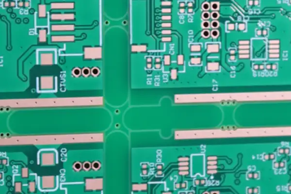
Not long ago I wrestled with a PCIe Switch PCB, and just finding a suitable board factory took nearly two months. Many people think making multilayer boards now is just finding a multilayer PCB supplier and sending a Gerber, but if you have really run 16GT/s and above, you know the loss hurdle cannot be fudged. At first, to save trouble, my board used a conventional high speed PCB manufacturer, who claimed to be able to control impedance, but the prototypes came back with the eye directly closed. Chasing it to the end, the problem was not in the stackup design at all; it was the copper foil.
Copper foil is a thing which, though all called copper, at a 32GHz rate, the roughness of the skin almost decides how far a signal can travel. Later I sliced a board for a cross-section, and the conventional electrodeposited copper foil was as rough as sandpaper, with skin effect squeezing all the high-frequency current onto the pitted surface, so the actual path was longer by no small amount. Although that factory also claimed to make thick copper boards and could supply heavy copper PCB suppliers, the high-speed area should not use their standard copper foil at all. After that, whenever I put out a PCIe board, I must ask clearly about the Rz value of HVLP copper foil; below 3 microns we can talk, and ideally below 2 microns. In fact many multilayer PCB manufacturers themselves may not understand this; when you speak with their CAM engineers, they only repeatedly emphasize line width and spacing and do not mention the conductor loss part at all.
Things went much more smoothly after I switched to those HDI PCB suppliers that specialize in chewing on high-loss materials. Because they routinely make laser blind vias and any-order interconnect boards, they are more sensitive to dielectric loss itself. What impressed me most was an HDI PCB manufacturer for high-speed backplanes who replaced all the core signal layers with low-Dk base material, and cut loss almost in half. Although the price doubled, for traces longer than 5 inches, not using ultra-low-loss material is a dead end, with no room for compromise at all. The PHY inside a PCIe Switch chip is strong, but once board-level routing grows long, the channel budget is eaten entirely by copper foil and dielectric, leaving almost no margin for jitter and crosstalk.
Looking back now, the most to be feared in making this kind of board is going to a thick copper PCB manufacturer that only makes power boards to discuss high-speed area requirements. Their strength is stacking copper thickness, dealing with hundreds of amps of current, but you simply cannot use that thick copper on high-speed signal layers; once the surface copper thickness goes up, the etch factor gets worse, line width control becomes poor, and loss deteriorates sharply. My habit now is to let a heavy copper PCB manufacturer play to its strength in the power area, pulling copper thickness to 6oz or even 10oz without problem, while concentrating all high-speed differential pairs on a separate inner layer with ultra-thin cores and HVLP copper foil, and then handing the whole stack to a multilayer PCB supplier who can master both ends. There are not many such factories, but once you find one, your PCIe link debugging is basically half successful. That kind of pain of high speed and thick copper being incompatible is in fact only because you have not found a board factory able to handle both types of process.
Loss, put plainly, is an account between materials: if you save money on copper foil, instruments, time and revision costs all come back to be paid. Now when my boards go out, I really dare not save money on high-speed lines; I stack on all the good material I can, because once on a cabinet, if the eye will not open it is just junk, and nobody listens to your explanation that the board factory’s process was not good enough.
Recently, on a PCIe Switch PCB project, I was nearly driven to doubt life by the matter of copper foil. The client insisted at first on a copper foil said to have extremely low roughness, with a beautiful parameter sheet; simulation showed it could save a few tenths of a dB of insertion loss, and it felt like a long trace would just fit the edge of the link budget and it had to be this foil. But when I truly handed the board to a high-speed PCB manufacturer who advertised high-frequency experience for prototyping, the problem arrived.
That high speed PCB manufacturer reported that this copper foil had been pre-treated too restrainedly, and local blistering appeared in their thermal stress test after lamination. At first I thought their process capability could not keep up, so I asked another larger multilayer PCB supplier, and the engineer in turn asked me: have you considered peel strength data? At that moment I realized that roughness is not something to reduce blindly; it is bound to reliability. The bond between copper foil and prepreg depends on that micron-level physical anchoring. Once ground too smooth, subsequent thermal cycling, reflow, and even the mechanical stress produced by long-term operation of the board installed in a chassis may quietly crack the layers apart. This kind of failure does not appear immediately, but it is more deadly than insertion loss exceeding the limit, because even basic connectivity is gone, so what is the point of talking signal integrity.
Later we backed off the copper foil scheme by one step and selected a copper foil with a special passivation treatment on the surface, with noticeably better roughness than the common RTF on the market but not of the extreme ultra-low-profile type. When building the board, we specifically had the multilayer board manufacturer provide measured surface roughness values for every batch, and also spot-checked peel strength. Many HDI PCB manufacturers can in fact do this, depending only on whether you raise the requirement. If you do not discuss it, they default to the most conventional copper foil in their library, and it is even possible that the foil used by the same multilayer board manufacturer this time differs from next time, as long as it meets the minimum IPC standard. But high-speed links really cannot be played like this; nobody can bear drift in batch consistency.
That was not all. Another board involved large current and needed thick copper, so we had to look for a supplier capable of thick copper boards at the same time. This time we were forced to face another contradiction: the roughness of heavy copper PCB is naturally high, and the thicker the electroplated copper, the more obvious the surface profile, and the harder it is to ignore its influence on high-speed signals. We asked several heavy copper PCB manufacturers, and basically as soon as you said you wanted 6oz copper and also wanted roughness control, the other party began to stammer. Later we found a factory that made thick copper PCBs and also had high-frequency experience. It relied on a selective plating process, thickening copper only in the power area while the logic area kept standard thickness copper foil, which barely achieved a balance. This kind of cooperation requires you to plan the areas from the layout stage and physically separate power networks and high-frequency signals, otherwise even the board factory cannot make it.
The whole process taught me one thing: when choosing an HDI PCB supplier or multilayer board supplier, never look only at whether their website has high speed and low loss on their lips. You must go and see their copper foil pretreatment line, and ask clearly what surface treatment lowers roughness without damaging adhesion. Some factories use chemical roughening and some use micro-etching plus passivation, and the difference in process routes directly decides the reliability performance of the final copper foil. Also, do not fantasize that one kind of copper foil can be used for every design; for a mixed-signal board like a PCIe Switch, you may well have to negotiate with the board factory on the same board for a hybrid copper foil scheme, using different foils on different layers. The engineering communication cost added in the middle is far greater than choosing a so-called top-grade copper foil material, and it is often the real watershed that decides whether a project can land.
Over the years of dealing with PCIe Switch boards, I have had a love-hate relationship with stubs. Many people think that as long as you find a reliable multilayer PCB supplier and throw the parameters over, everything is done, but differential signals above 32Gbps simply do not give way to sentiment. Last year I fell on a PCIe 5.0 switch board where, of 8 lanes, two eyes would not open no matter what. After a long investigation, it turned out to be the stub left in the via that was not backdrilled clean, which created a resonance near 22GHz and dropped differential insertion loss by almost 8 dB. Later we reflected on the pain and worked with the HDI PCB manufacturer we cooperated with to regrind the process, compressing backdrill accuracy from plus or minus 6 mil to plus or minus 3 mil, and kept the stubs of all high-speed differential pairs on the board within 5 mil before the signal could be pulled back.
I tell this not to say that stubs are so deadly, but because I found that many people underestimate the perturbation of physical structure on signal modes. Once an inner-layer differential pair is asymmetric, or the reference plane suddenly lacks a piece when the via changes layers, common-mode components appear at once. Last year I tested a power-carrying board made as a Thick Copper PCB that routed a group of PCIe 4.0 differential lines at 3oz copper thickness. The etch sidewall angle made the impedance of the two lines differ by nearly 3 ohms, and as a result the link repeatedly downshifted to 8GT/s during the training phase. I went back and forth with that heavy copper PCB manufacturer, who felt that a difference this small did not matter, but when we scanned S-parameters with a VNA, mode conversion Scd21 clearly turned up above 16GHz, and how could the receiving end not suffer.
Now, for any multichannel PCIe switch board, I look at only two things when selecting a multilayer board supplier: first, whether they dare to put out the measured data of residual stub length after backdrilling; second, whether they have cross-section analysis capability for differential pair impedance control. Some HDI PCB suppliers advertise any-layer interconnect and stacked microvias, but when asked about inner-layer copper thickness uniformity and dielectric thickness tolerance of the differential pairs, they start to play dumb. The high-speed PCB manufacturer we mainly cooperate with now attaches a TDR test report and cross-section photos of backdrilled holes to every batch, and the distribution of stub lengths is clear at a glance. In this day and age, I dare not put a 32Gbps differential line on a board from a factory that lacks transparent process data.
There was also a rather counterintuitive feeling: thick copper and high speed are not irreconcilable. Earlier I made a board for an industrial switch with a current requirement up to 40A, and we had to use 2oz thick copper. That heavy copper PCB supplier initially gave a differential pair model that did not consider the insertion loss increment from copper foil surface roughness at all, and the measured result was nearly 2dB worse than simulation. Later we changed to a multilayer board manufacturer willing to do electron microscope analysis of roughness and swapped the copper foil type from reverse-treated to low-profile copper, and the loss immediately dropped, with almost no more abnormal resonance below 20GHz. So when a board reaches this rate, if any one of stubs, copper teeth, dielectric and alignment accuracy slacks off, it will be deadly. As long as the factory is reliable, we designers save a big chunk of worry; otherwise we are flipping between eye diagrams and S-parameters every day, and I do not want to live that kind of life again.
I have handled several PCIe Switch PCBs, and honestly the biggest headache at the start was not trace length matching but finding a reliable manufacturer to land the board. The density of high-speed signals and the BGA area is such that conventional multilayer PCB manufacturers dare not guarantee anything, especially when you need backdrilling or resin plugging; many multilayer PCB suppliers shake their heads and say yield cannot be achieved the moment they see the drawing. Later I learned my lesson and communicated with an HDI PCB manufacturer at the earliest stage, because their process route is more adapted to designs with small pad sizes and perverse interlayer alignment requirements. The pit here is that some factories carry the name of a high speed PCB manufacturer but their control of differential via impedance actually remains at NRZ-era experience, and the moment PAM4 runs it is exposed immediately.
Once the layer count passes 16, signal quality is no longer the only pain point; the real stranglehold is the combination of heavy copper and thick copper. Many people only stare at routing when designing and forget that power layers need heavy copper to carry transient current. When looking for a heavy copper PCB supplier, you will find that those who can make thick copper and those who can make high speed are often two kinds of factories, and nationwide only a few can combine the process of a thick copper PCB manufacturer with high-speed lamination. Once we raised power layer copper thickness to 4 ounces, and the board warpage collapsed outright. After two rounds of rework we honestly switched to local thick copper plus inner-layer heat dissipation copper blocks, and settled it only after going back and forth with the HDI PCB supplier over parameters. So when I discuss BGA fan-out now, I casually determine the copper thickness and lamination structure of the power and ground layers in advance, otherwise there is rework everywhere afterward.
On the via matter, many people agonize over how long the backdrill stub is, but I believe what takes more experience than absolute stub length is the shape of the pad transition region. For a 0.4mm pitch BGA, if the pad is slightly larger it pulls the impedance of the adjacent differential pair off, and such a local mutation shows up in simulation as a little spike in step response, directly shrinking the eye. I personally prefer to have the multilayer PCB manufacturer remove non-functional pads directly and hollow out the reference layer under the pad slightly. The cost is one more alignment accuracy control during processing, but impedance continuity is much better. This also exposes a reality: many so-called HDI PCB suppliers do not do hollowing optimization at all; they think connecting the line through is the end of it, and any engineer who understands a bit of signal integrity will get stuck on this.
Finally, on the reference plane, I have stepped in more mines than on routing. On a 12-layer PCIe Switch PCB, vias clustered at the edge of the transceiver, the return path was cut to pieces, and link training failed intermittently. At that time, after ruling out static and power noise, I found that a thermal notch had been opened in the plane layer beneath a BGA pad, and the return current detoured a big circle. Later we changed to a multi-ground-plane stack and asked the heavy copper PCB manufacturer to extend the copper into a whole piece in that region, and the problem disappeared. Now when I make this kind of board, I would rather spend more on board material than fail to ensure the plane layers are complete enough; otherwise debugging can never find the culprit.
Not long ago I wrestled with a 96-lane PCIe Switch PCB, and only after laying out the board did I find that just making those several hundred differential pairs lie down obediently was enough to drink a pot. The switch chip pins are as dense as sesame cake, the traces are squeezed together, and they have to change layers at every turn. Layer changing itself is no capital crime, but what is deadly is that reference planes get cut to pieces, and once the return path is disordered, link training later shows its face directly. In the phase of finding a multilayer PCB supplier I suffered at first: out of greed for cheapness I chose an ordinary multilayer board factory, and as a result the coupling of ground and power planes was loose and slack, the signal eye looked like crumpled waste paper, and the whole board could only be scrapped.
Later I learned and simply went to find a factory that specializes as a high speed PCB manufacturer to re-prototype. Their control of interlayer alignment and dielectric thickness had clearly gone up a notch, and low-roughness copper foil was specially chosen, so trace loss visibly fell. But what really made me remember was not the signal layers. This switch board had to carry large current, and the core power section had to be processed with thick copper, but those generally labeled heavy copper PCB suppliers on the market often cannot balance fine routing and thick copper: either copper thickness is pulled up but line width and spacing cannot be made fine, or the fine routing is done but the copper thickness is falsely labeled. In the end, after circling around, I found a thick copper PCB manufacturer that could truly handle thick copper without losing precision. Using the clumsy method of stepwise plating plus controlled-depth routing, they stubbornly made 70 micron copper in the power area and fine lines in the dense BGA area on the same board. Cost more than doubled, but the voltage drop and temperature rise were finally pressed down.
Many people feel that length matching for multilane switches can be done by winding serpentines, but anyone who has done it hands-on knows that is self-comfort. To keep impedance consistency on that board, I would rather have the sixteen differential pairs of an x16 port arranged with a symmetric topology in the BGA breakout area ahead of time than let any pair wander and wind out a long extra stretch. Because even with the best HDI PCB manufacturer, one more bend means a little more additional dielectric loss, and once lane-to-lane loss deviation widens, even elastic buffers cannot tolerate it, and the training phase will directly downshift. Put plainly, PCIe Switch PCB design is a constant trade with physical limits: if you want many lanes, you pay with layout density and layer count; if you want thick copper to carry current, you must hold your nose and accept the concession in line precision. Whether choosing a multilayer PCB manufacturer or an HDI PCB supplier, it is just finding out who can find in these mutually conflicting needs that balance point that does not drive you crazy.
Back when I made a PCIe Switch board, I always felt that as long as the schematic was correct and the trace length matching was calculated precisely, the rest could be thrown to the board factory. In fact it is not like that. At that time my company dealt with several multilayer PCB suppliers at the same time: some specialized in consumer thirty- or forty-layer boards, and some carried the name of a high speed PCB manufacturer but mainly made backplanes. Later I found that when the same design was handed to three factories, the differential impedance dispersion that came back differed by a large margin. Especially when your link goes to PCIe with PAM4 modulation, the sensitivity to reflection is simply not something that adjusting a few mil of routing can bring back; it is directly bitten dead by the fiber weave and resin distribution of the PCB material.
Later I made two trips to factory lines specifically and watched how they handled hybrid lamination, and I figured out why some heavy copper PCB manufacturers are very stable making power boards for others but become chaotic once switched to high-speed digital boards. The etch factor of the heavy copper layer is not on the same scale as the inner signal layer copper thickness, and after lamination, once the wetting of the glass cloth is uneven, that 2oz copper plane becomes a reflector that should not appear in a microwave anechoic chamber. If you find a thick copper PCB manufacturer who also takes heavy copper, in theory he can make power layers 6oz or even 8oz, but you need them to understand the eye margin of PAM4 at the same time, which is almost asking a man who swings a big knife to repair a watch, and many factories are not a match.
So now when you ask me to choose an HDI PCB supplier, what I care about is not how many layers they can do but whether they have done mixed-rate schemes like PCIe Switch PCB. Some HDI PCB manufacturers have good laser drilling aperture control and clean microvia stacking, but their copper filling process and glass cloth cutting method have almost no accumulated data on the effect on signals above 32Gbps NRZ. If you ask for an impedance prediction, they hand you a polarization curve drawing back and forth, and do not even mention timing skew under the glass weave window effect, which is very deadly. In a multilayer board, the requirement of the layers PCIe runs through for dielectric uniformity is honestly far more important than pure laser machining capability.
I have even encountered a case where the second batch of boards prototyped by the same multilayer PCB manufacturer changed the copper thickness of the power island from 1oz to 2oz without telling engineering, and the resonance point of the whole board shifted, and the PCIe 6.0 link BER went directly to unrecoverable. After that I insisted that for any PCIe board, especially those using thick and heavy copper, do not look only at the machining capability a supplier writes on its website; make them produce cross-section reports where signal integrity verification was actually done against your stackup, otherwise you are gambling. High-speed PCB manufacturers and heavy copper PCB manufacturers are very often just two different species, and finding repeatability in both at the same time is far harder than drawing an equal-length line in simulation software.
Speaking of PCIe switch work these days, I increasingly feel that the textbook-style power partitioning ideas are often making simple problems complicated. Especially with high-power switch chips, like Gen5 or even Gen6 parts whose power easily reaches twenty or thirty watts, if you are still agonizing over drawing a separate power copper for core voltage, SerDes voltage and I/O voltage, it is easy to tangle yourself up instead. I have seen many boards where the problem in the end was not power noise but that the ground plane was cut to pieces, the return path of high-speed signals was truncated, and the eye was flat on its belly.
So in recent years I have dealt with heavy copper PCB manufacturers a lot and become accustomed to changing course: on the premise of satisfying current carrying, use a whole large copper pour as a common carrier for multiple power supplies, then achieve isolation by placement and decoupling capacitors. It sounds a bit like a wild approach, but think about it: the power domains of the modules inside the switch chip itself already have considerable suppression ability, and excessive partitioning at board level often costs more than it gains. In particular, finding the right multilayer PCB supplier is important; some factories have a very good understanding of the thick copper process and can make 3 ounce or even thicker copper on inner layers for large-current power layers, with a heat spreading effect far better than simply cutting planes.
Power consumption is a thing where we often focus too much on the chip’s nominal TDP and ignore that the board-level thermal spreading path is the real bottleneck. Once I worked with a thick copper PCB manufacturer, and the switch chip on that PCIe switch PCB had maximum power consumption close to 22 watts. We did not use an exaggerated heat sink; instead we relied on inner-layer thick copper and a dense thermal via array to pull the heat directly from the package bottom to a large copper area on the back, together with natural convection of the system chassis, and the junction temperature was stubbornly more than six degrees lower than simulation. This reinforced an idea in me: thermal design is not about throwing the chip to a heat sink and being done; the PCB itself is the best heat sink, especially once you find a reliable high speed PCB manufacturer who knows how to find the balance between high-speed routing and thick copper, controlling impedance while spreading heat capacity.
Some will say: are you not afraid of the analog ground being disturbed by the digital ground? In fact, for switches that run above PCIe Gen4, the isolation strategy inside the chip is already fairly mature, and forcibly splitting the ground plane at board level easily creates additional common-mode noise where it crosses the split. I tend to let one complete ground plane carry all returns and then physically isolate sensitive circuits by device placement. For example, I gather the reference clock and PLL supply of the SerDes on one side of the chip, away from high-current switching supplies, instead of drawing a trench on the ground layer. Under this idea, finding the right HDI PCB supplier becomes the key, because to squeeze so many high-speed differential pairs and thick copper power layers into a limited board thickness, laser blind vias and any-layer interconnect capability decide how far you can go. If an ordinary multilayer PCB manufacturer cannot do third-order or even any-order HDI, many ideas cannot land.
At the end of the day, power management on a PCIe switch board is not an arithmetic problem; it is a game of space and path allocation. The more plane area you allocate to power, the less complete reference layers may remain for signals; the more vias you stuff under the chip, the better the heat conduction, but the more it may destroy the routing channel of differential pairs under the BGA. Working together over the past few years, the HDI PCB manufacturers who can truly handle this contradiction usually have enough stackup experience and material databases. They know which resin systems have small loss tangent changes at high temperature, and they know that a via filled with copper paste can have thermal conductivity an order of magnitude different from one filled with resin. These details are far more useful than the simple dogma do not let power cross a split.
I think in future, as chip process nodes advance and single-lane rates continue to double, the transient current pulses of switch chips will become steeper, and the ratio between peak and average power will be pulled larger. By then, sticking to the traditional multi-power-domain partitioning approach, the inductance of the power supply network may not hold. Instead of spending effort cutting planes, it is better to pull in heavy copper PCB suppliers early and study how to make the power copper thick enough and the paths short enough, or even consider embedding copper blocks inside the PCB. Some things you only figure out, the paper behind the window, by truly making a few boards of 16 layers or more, burning a few chips and paying a few rounds of tuition.
Earlier I made a switch board for a data center with two PCIe Switch chips on it, and with 48 lanes of links drawn, I knew halfway through that this time it could not be muddled through on an ordinary PCB. That board finally used 14 layers, with three cores stacked with blind and buried vias, with most signal layers using Panasonic M6, and after the whole board was prototyped and came back, my first action was not to power it up but to scan the impedance of the differential pairs with TDR first.
Many people think copying the layout guide in the chip datasheet once is the end of it, but once signals run above 16GHz and board thickness exceeds 2 millimeters, things begin to go out of control. I once sliced an unsuccessful board whose factory was a multilayer PCB manufacturer that would say anything was fine verbally, and the result was that inner-layer copper thickness tolerance drifted by nearly 15%, differential line impedance was off to 108 ohms, and link training failed outright. Later I found a multilayer PCB supplier that was not large but specialized in exactly this, whose interlayer alignment could be made plus or minus 2 mil with stable dielectric thickness batch consistency. The same stackup parameters, projected again, and the eye opened immediately. After that I formed a habit: for boards with high-speed differential signals above 8GHz, I first confirm with the PCB factory whether they have made backplanes or switch motherboards of the same level, and a sentence like high speed pcb manufacturer on their website is useless; they must produce cross-section reports of past mass production for me to see.
There is another layer of trouble in the power supply. The SerDes power rails of a PCIe Switch chip are basically around 0.8V, with transient current jumping very sharply. If only ordinary 1oz copper thickness plus a few capacitors are used to muddle through, the voltage drop in dynamic switching is big enough to cause unrecoverable link packet loss easily inside the chip. The core power of my board used local 3oz thick copper, and I directly found a heavy copper PCB manufacturer that could do the embedded copper block process: not the kind of play where only the surface layer is thickened, but where the inner power plane truly raises copper thickness to 3oz, so that internal resistance drop could be controlled below my psychological expectation. Later, in the batch stage, to reduce cost I tried a heavy copper PCB supplier whose price was thirty percent cheaper, and as a result the elongation of the inner copper foil was insufficient, and after more than two hundred thermal cycles, micro-cracks appeared at the interface between copper and resin, which forced a revision and a return to the old supplier’s thick copper process.
Routing density also pushed me toward HDI. Fan-out at 0.5mm pitch under the BGA, if done on a through-hole board, would have the inner layers gnawed ragged by antipads and all signal return paths broken. My first version used a stacked-via any-layer interconnect design, and I found an HDI PCB manufacturer specializing in high-order HDI who could stably make three layers of stacked vias without cracking, with fill dimple controlled within 15 microns, data I never obtained from other HDI PCB suppliers. Later, when peers asked me how to select HDI factories, my answer was simple: do not listen to sales tell you about equipment lists; ask directly how much sampling of filled-via cross-sections they do every month, and how often they analyze the plating bath chemistry. These details are more practical than any verbal promise.
At the end of the day, to combine high-speed signals, large current and ultra-high routing density in such a high-layer-count board, the hardest part is not design technique but finding the right factory. You draw a nice PCB with 256 differential pairs of a PCIe Switch, needing 3oz inner copper and two-order HDI, and if you split these needs and look for different suppliers to patch together, there will certainly be trouble. What I want is one factory that can string together the dielectric control capability of a high speed pcb manufacturer, the resin flow control of inner thick copper of a heavy copper pcb manufacturer, and the stacked via yield of an HDI pcb supplier. Even if the unit price of such a multilayer pcb manufacturer is a notch higher, it is far more cost-effective than repeated revisions. Chips and power can be replaced and upgraded in place, but once the foundation of the PCB is chosen wrongly, the schedule and signal quality of the entire project will be dragged to death on the board factory’s production line, and this is a pit I really do not want to step in a third time.
I have stepped in quite a few pits on PCIe Switch PCB in the past two years. The market is constantly talking about ultra-low-loss laminates and HVLP copper foil, as if stacking material would get a PAM4 32GHz channel to run through. But if you actually communicate in depth with multilayer board manufacturers a few times, you will find it is not like that.
In one case I handled, a 64-port switch, the first multilayer board supplier I found immediately recommended top-grade material, with Df pressed below 0.0019. The first version came back and the eye jittered beyond viewing. After checking around, the problem was neither in the material nor in the via stubs; the reference layers of the whole board had been cut to bits by power splits. This made me ponder again many default rules in PCIe 6.0 design. One of the big misconceptions is simplifying the high-speed link problem, as if managing insertion loss alone settles everything. PAM4 is an order of magnitude more sensitive to reflection than NRZ, and a slight oddity in impedance continuity makes EVM collapse directly. And the advice that HDI PCB supplier later gave me was that rather than repeatedly winding for equal length on the routing layer, it would be better to re-optimize the shape of the decoupling capacitor pads under the BGA to reduce impedance discontinuity points. This view is rarely mentioned in traditional signal integrity checklists.
Another common dead end is thinking a PCIe switch is no different from a graphics card or network card and copying the via design from Gen4. The Gen6 PAM4 presses tolerance to intersymbol interference to the limit, and a 20 mil stub that in NRZ could perhaps still be endured with emphasis eats half the eye height outright in PAM4. A high speed PCB manufacturer I worked with ran a comparison test and tightened backdrill accuracy from plus or minus 4 mil to plus or minus 2 mil, and the improvement in eye opening was not just that number in simulation: measurement showed a difference of 20% in margin. This is not a selling point of process capability but a hard threshold that physics cannot bypass.
Speaking of serpentine length matching, this is also a hard-hit area. To match groups, multichannel switches often wind dense serpentine lines on the board, which destroys the lane-to-lane loss consistency completely. On a 15-inch channel, winding out 2 inches of extra trace directly eats an extra 1.5dB of loss, and the eye of such a port will close visibly faster than other channels. The real solution should be to plan connector pins and BGA escape with symmetric topology in the front-end to eliminate skew, instead of patching up after fan-out on the surface layer. I have a module that was done exactly this way, without even using the any-layer interconnect of an HDI PCB manufacturer, relying only on conventional through holes plus backdrilling, and lane skew was compressed to within 3ps by topology optimization.
The coupling of heat and electricity hides the deepest here. Many people consider the job done once the heat sink is buckled on, forgetting that the temperature gradient caused by the switch chip’s 20-plus watts of power makes the Dk value of the base material drift in the horizontal direction, so the delay parameters that were originally matched are all scrambled. Later I settled on that heavy copper PCB manufacturer for the power layers, not only for current carrying but more for the heat spreading effect of the thick copper layer, which spreads out hot spots under the chip, lowers DC voltage drop and incidentally smooths the thermal gradient a lot. Many multilayer PCB manufacturers claim to be able to do this kind of thick copper board, but those that truly handle pressing voids and resin loss caused by uneven copper thickness are only a few. Choose the wrong supplier and the risk of inner-layer short circuits doubles.
Some ask why not use an all-HDI stack, with laser holes directly on the pad being so clean. My personal view is that for a large-area, high-heat-consumption board like a PCIe Switch PCB, blindly going to any-layer HDI only doubles cost with limited benefit. Unless your channel density is so high that you must use microvia breakout, an improved build-up method combined with backdrilling can hold signal quality just as well. Instead, some HDI PCB suppliers, to demonstrate technology, over-design the stackup and stack alignment deviations from multiple lamination cycles on top of an already complex channel, which is more loss than gain.
At the end of the day, running PCIe 6.0 signals is never a breakthrough at a single point in one link. It tests how finely you understand the whole physical link, from the copper thickness tolerance given by the Thick Copper PCB manufacturer, to the etch accuracy of the connector pad, all the way to the substrate vias of the chip package.
People who make high-speed boards often draw a PCIe Switch PCB as an ordinary digital board, looking only at differential impedance and length matching and calculating power as a static load and calling it done. In fact my deepest feeling over the years is that the transient behavior of the power distribution network is far more deadly than trace details, especially in scenarios involving multi-lane simultaneous training or deep ASPM switching. Once, on a 12-layer board, we laid out a 48-lane switch chip, using the stackup provided by a high speed PCB manufacturer with M6-grade material, and the routing eye looked quite pretty, but link training would randomly produce ts1 timeouts. Finally the problem was located not on the differential lines but on several inner power planes that could not keep up with load jumps within tens of microseconds; VDD sagged a notch, causing the SerDes PLL to lose lock.
After that project, whenever I make a PCIe Switch PCB, I first align the transient current swing with the people making the power solution in advance and then use that worst-case swing to constrain the DC resistance of the planes and the decoupling network. The default plane partitioning that many multilayer PCB manufacturers give is to cut wherever convenient; they do not care about the step response of tens of nanoseconds on the return path. But the eye is eaten by exactly these things, especially for low-swing PAM4 on PCIe 5.0 and 6.0, where a slight collapse in power ripple makes the bit error rate explode directly. So when I look for a multilayer PCB supplier now, I value whether they can cooperate on power integrity simulation, not only hand over a stackup impedance table.
Another often underestimated item is the contradiction between thick copper and high speed. Some boards, to carry large current, require 3oz or even 6oz thick copper on power layers, and if you casually find any heavy copper PCB supplier to make it, the high-speed differential pairs will certainly flip over. The sidewall profile and conductive modulus differences of thick copper etching degrade differential pair insertion loss and phase consistency, and above 32Gbps NRZ, the glass fiber weave of the dielectric layer also affects delay more obviously. My practice now is that if the on-board power truly needs a large cross-section, I would rather use one or two more layers of 2oz copper with controlled dielectric thickness than make a single ultra-thick copper layer. A thick copper PCB manufacturer usually understands thermal management and current carrying better but not necessarily high-speed signals, so it is unrealistic to expect them to control smooth transition from pad to line for you, and you have to write details like pad and antipad size and removal of non-functional pads into the fab notes yourself.
Speaking of pads, in fact the impedance discontinuity of PCIe connector gold fingers and AC coupling capacitor pad surfaces is the root cause of high-frequency parameter shifts in many boards. I have seen quite a few HDI PCB manufacturers claiming capability of 32G whose sample laser blind via dimples were too large, with residual stubs exceeding 8 mil, and they were scrapped on the spot. Now when I meet a high-density PCIe Switch design, I first consider whether to go with an any-layer interconnect HDI scheme, because laser drilling accuracy can help me compress the stub below 4 mil, at the cost of soaring expense. But if the process stability of the HDI PCB supplier is insufficient, yield in later volume production will be very ugly. You have to confirm whether their backdrill depth tolerance can hold plus or minus 3 mil and whether surface copper thickness uniformity after resin plugging is consistent.
I do not think routing is that mysterious: just control intra-pair skew of differential pairs honestly within 4 to 5 mil, do not be stingy in pulling differential pair spacing apart and isolating with ground vias, and the rest depends more on the material itself. For differential pair intra-pair length matching, I basically no longer force serpentine winding, because phase difference compensation produced by winding easily introduces mode conversion above 16GHz. I will fight early in layout for SerDes channels to have paths that are as straight and short as possible, and also have the multilayer PCB supplier stagger the glass fiber direction from the trace angle, which saves a lot of trouble. All in all, if on a PCIe Switch PCB you only get the differential lines through, without digging into power transients, without managing the pull of thick copper areas on high-speed signals, and without handling impedance mutations at pads, then the measured results will certainly not be what the signal integrity simulation said.
On PCIe Switch PCB work, I increasingly feel that the margin left for power consumption and power supply is more likely to roll over than signal integrity. I once had a switch board whose idle power was only three or four watts and looked warm; but once switched to full load, thirty-odd watts surged up instantly, and while ASPM low-power states bounced back and forth, the power distribution network simply could not catch its breath, and the voltage dip directly reset the link. I paid for this, and in later designs I learned: I went directly to a multilayer PCB manufacturer to make the power layers thick copper at the stackup stage, but conventional board shops generally only give 1oz, which cannot carry that kind of step current at all, so I specially switched to a heavy copper PCB manufacturer and had them use 4oz copper for two main power layers and an inner ground layer in a 12-layer board. With the ground path resistance lowered, the junction temperature was pressed down.
The high-speed part is different again. SerDes routing is easily dozens of pairs, and PAM4 is fragile to begin with; the eye was messed up by via stubs and return flow fragmentation. Later I contacted a high speed PCB manufacturer to help me squeeze all routing into inner layers close to a continuous ground plane, laying ultra-low-loss material on key layers, while low-speed and power layers were hybrid-laminated with ordinary FR-4 to save cost, though I had to simulate the impedance turn at the material boundary honestly. When the board got dense, BGA fan-out was a headache. I asked around among HDI PCB manufacturers, and most told me that laser blind vias cannot be mixed with thick copper above 4oz. Later I found an HDI PCB supplier that could take this mixed process, using a half-buried blind via structure to separate the high-density area from the thick copper power layers, so that current carrying capability was not sacrificed.
Power plane splitting tortured me even more. At first I cut the I/O power and core power into bits and pieces, thinking the isolation was good; actual measurement showed that one group of differential pairs crossed two power domains underneath, the return path ran wild, the skew between channels directly exceeded 0.6ps, and most of the eye closed. Later I readjusted with the multilayer PCB supplier, retreating the area under high-speed routing entirely to a complete ground plane and moving all power splits to the low-speed areas on the two sides of the board, and I pressed the transient margin directly according to maximum load by an extra twenty percent, while the thermal simulation also incidentally scanned the thermal gradient problem together. Looking back now, even if you invite a heavy copper PCB supplier that can do thick copper, or a thick copper PCB manufacturer capable of 6oz, however fancy the process, it is not as good as thinking through power integrity and thermal design together; otherwise changing to a more expensive board factory only plates the pit with a layer of gold.
An SD-WAN hardware project showed how complex these boards really are: in
Several fabricators turned down our 38-layer TPU PCB. Splitting it into a
How grounding, power-loss release hardware, and multilayer or HDI fabrication decide whether
- Pienten ja keskisuurten erien tuotannon asiantuntija
- Korkean tarkkuuden piirilevyjen valmistus ja automatisoitu kokoonpano
- Luotettava kumppani OEM/ODM elektroniikkaprojekteihin
Aukioloajat: (ma-la) klo 9:00-18:30.
Get quote, solution or any question, Andre always here to help