
How Do PCBs for Medical Devices Hold the “Last Line of Defense for Life”?
In the field of medical electronics, attention often focuses on complex algorithms;
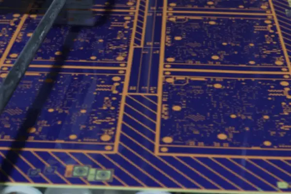
PCBs are truly fascinating components. I recall a visit to a factory in Shenzhen where I observed the entire HDI PCB manufacturing process. Workers, clad in cleanroom suits, operated machinery within the “Yellow Light Zone.” The sheer level of precision I witnessed made me realize that the simple green circuit boards I used to see when dismantling old radios as a child belonged to a completely different realm of technology. Indeed, modern high-end manufacturing demands this level of meticulous craftsmanship—precision measured in microns.
Domestic manufacturers specializing in high-speed PCBs have made particularly significant strides over the last few years. An engineer acquaintance of mine mentioned that, just a decade ago, he frequently had to spend time explaining the critical importance of impedance matching to clients. Nowadays, however, many clients are capable of articulating their specific technical requirements on their own. This shift is reflected not only in the precision of the final products but—more crucially—in the industry’s fundamentally heightened focus on technical details.
I was once deeply struck by a specific case study regarding PCB board printing. A domestic firm had been commissioned to customize a high-speed circuit board for a European client. Initially, the client approached the project with a degree of skepticism. However, once the test data came in, it revealed that the board’s signal loss was actually 0.5 dB lower than that of their German supplier. This incident reinforced my belief that the upgrading of the manufacturing sector cannot be achieved merely by chanting slogans; rather, it must be built upon the steady accumulation of concrete, technical breakthroughs.
In fact, the transition from manufacturing standard PCBs to designing high-end boards is much like practicing calligraphy. At the outset, one might assume that simply ensuring the electrical connections are established is sufficient. However, to truly excel at it, one must delve into deeper complexities—such as signal integrity and thermal management. I have observed smaller manufacturers undergoing this transition with great difficulty, as they are often compelled to completely dismantle and rebuild the established practices they had grown accustomed to.
I recently had a chat with a friend who runs a hardware startup. He mentioned that, nowadays, he actually feels more at ease sourcing complex circuit boards from domestic suppliers—and not merely because of the cost. Rather, it comes down to communication efficiency. If a requirement is sent over in the middle of the night, an engineer can respond immediately. This kind of seamless coordination is often difficult to achieve with overseas partners.
Progress in manufacturing is often reflected in these subtle details—much like the delicate control of heat when cooking. An outsider might not spot the nuances, but an expert can tell instantly whether the craftsmanship is truly up to par.
I’ve long felt that designing circuit boards is becoming increasingly akin to creating a work of art. I only truly realized this a few days ago while helping a friend revise the mainboard design for a smartwatch—I had originally assumed it would be a simple matter of tweaking the placement of a few components.
That design revision reminded me of the traditional PCB printing processes I encountered when I first entered the industry. Back then, even producing a double-sided board felt incredibly complex. Nowadays, a typical HDI PCB used in any smart device can easily feature a dozen or more layers of circuitry stacked tightly together.
I once visited a factory to observe their high-speed PCB production line, and it was a fascinating experience. I was particularly struck by the look of intense concentration on the face of a veteran technician as he inspected the circuitry through a magnifying glass. He told me that their biggest fear these days isn’t the density of the wiring, but rather misalignment issues.
In truth, I find that the most frustrating aspect of the job right now is that the design software constantly lags behind our actual practical requirements. Lines that appear perfectly crisp and clear on the digital schematics somehow end up riddled with issues once they reach the actual manufacturing stage.
I recall a project last year that required integrating an antenna directly onto the mainboard; it was an absolute nightmare. Even with the latest HDI technology at our disposal, we had to go through multiple rounds of revisions before we finally got it right.
Sometimes I find myself wondering why designing circuit boards has become such an arduous task. I eventually realized it’s because we’re constantly trying to cram too many functions into a limited amount of space—it’s like trying to squeeze an entire stereo system into a matchbox.
That said, there is still a tremendous sense of accomplishment in gazing at the intricate, densely packed circuitry inside a piece of precision equipment—especially when you realize that these hair-thin copper traces are what bring the entire device to life.
Lately, I’ve been experimenting with combining traditional manufacturing techniques with newer methodologies. The results have been quite promising—at the very least, it saves us from having to start from scratch and grope in the dark every single time.
Ultimately, I believe the most important thing in this line of work isn’t simply mastering a multitude of new technologies, but rather knowing how to apply the right solution at the right moment. After all, even the most advanced technology still requires human hands to guide and master it, doesn’t it?
Whenever someone asks me how to go about selecting a PCB manufacturer, I’m invariably reminded of all the pitfalls and mistakes I stumbled into when I was just starting out. I used to think that the newest equipment was the sole criterion for choosing a supplier, but I eventually realized that couldn’t be further from the truth.
I once encountered a supplier whose equipment list was packed with imported machinery, yet the HDI boards they produced couldn’t even maintain proper impedance matching. While their workshop did indeed house the latest LDI machines, their engineers hadn’t fully grasped the characteristics of the base materials; consequently, high-speed signals would suffer from reflection whenever they hit a corner. It is in moments like these that you realize what truly matters: whether the people operating the equipment can understand—and execute—your design intent.
Nowadays, I start by looking for evidence of long-term client relationships. For instance, if a PCB supplier for a medical device manufacturer can demonstrate a track record of consistent, high-volume deliveries spanning five years or more, that carries far more weight than any certification alone. I’ve seen small-scale suppliers—lacking prestigious certifications like AS9100 (Aerospace Quality)—who have spent seven or eight years producing high-frequency boards for drone manufacturers with defect rates lower than those of many major corporations.
The testing phase is often the easiest area for suppliers to cut corners. Some factories boast about having fully automated AOI inspection systems, but upon closer inquiry, you discover their actual sampling rate is less than 10%. A truly reliable supplier will proactively show you X-ray images of micro-via alignment data, or even use thermal imagers to demonstrate the temperature rise in high-current traces. During a recent visit, an engineer demonstrated their back-drilling process by slicing open a sample board right in front of me and using a microscope to point out the precise length of the residual stub; that kind of tangible, visual transparency inspires a level of trust that a mountain of certificates simply cannot match.
Environmental compliance has also become a key differentiator. During one factory tour, I noticed they were still using lead-based Hot Air Solder Leveling (HASL). When I mentioned that I needed boards for products destined for the EU market, the workshop manager immediately took me to see a newly installed Electroless Nickel Immersion Gold (ENIG) plating line. This kind of agile adaptability is the very core of modern manufacturing.
I’m currently working on a high-speed signal board project where the supplier suggested modifying certain traces to incorporate 45-degree angled corners, claiming it would reduce signal loss by a third. You won’t find optimization tips based on such real-world, practical experience in any standard process documentation. That is why, when selecting partners today, I place a much higher value on their ability to think beyond standard procedures and provide customized solutions.
Ultimately, finding a supplier is much like finding a doctor: a polished resume isn’t enough; what truly matters is their willingness to invest the time to analyze and address your specific, unique requirements. An exceptional PCB manufacturer should act as both a skilled artisan and a trusted consultant—someone who can look at your design schematics and suggest, “Adding a teardrop pad here would enhance reliability,” or “Routing a differential pair around that section would help mitigate power supply noise.” It is this depth of collaborative engagement that serves as the true foundation for high-quality PCB fabrication. I’ve recently noticed a rather interesting phenomenon: many engineers, when designing PCBs, seem particularly obsessed with pushing parameters to their absolute limits. For instance, if they see a board manufacturer advertising the capability to produce 2-mil trace widths, they feel compelled to design their boards to match that exact figure. I can certainly understand this mindset—after all, who wouldn’t want to make their product as refined and sophisticated as possible? However, after going through several actual prototyping cycles, I’ve realized that this pursuit often proves to be a case of diminishing returns. I recall one instance where, in an effort to reduce the spacing between components by a mere 0.1mm, our team repeatedly tweaked the routing on an HDI PCB; the result was that when the design went into mass production, the yield rate plummeted by 30%. It wasn’t until I spoke with the manufacturer later that I learned the truth: while their standard processes might boast high nominal specifications, sufficient headroom must be maintained to ensure stable yields during mass production. It’s much like driving a car—you can’t simply keep your foot on the gas pedal and run at maximum speed indefinitely, can you?
Speaking of silkscreen printing, I’ve certainly learned a lesson the hard way in that department. On one occasion, I was designing a palm-sized board that needed to accommodate dozens of components, leaving very little room for text placement. In a moment of youthful overconfidence, I decided to shrink the font height down to 0.6mm; the manufacturer subsequently reported back that the ink had bled, turning the text into an illegible blur. I’ve since learned my lesson, and now—no matter how cramped the layout might be—I insist on a minimum font height of 0.8mm. In truth, silkscreen text serves as more than just a label; it’s like fitting the circuit board with a tailored suit—it must be both clearly legible and entirely unobtrusive. For instance, I once saw a design where the silkscreen text was printed directly onto the “gold fingers” (the edge connectors)—which is essentially no different from sticking a label right onto your smartphone screen.
Regarding high-speed PCB design, I’ve come to believe that one shouldn’t get too fixated solely on technical parameters. I once worked on a batch of boards featuring RF modules where, in the initial stages, we focused so heavily on impedance matching that we completely overlooked the specific characteristics of the PCB substrate material itself. Later testing revealed severe signal attenuation, a problem that was ultimately resolved only after we switched to a different dielectric material. Sometimes, designing a circuit is much like cooking a meal: you can’t simply pile all the finest ingredients together and expect a great result; the key lies in how you combine and harmonize them. Nowadays, whenever I work on high-frequency projects, I make a point of prototyping the design using substrates of several different thicknesses for comparison—after all, even a millimeter-level difference in board thickness can have a significant impact on signal integrity.
I also had an experience visiting a PCB manufacturing facility that gave me a fresh perspective on the printing process. On the factory floor, a veteran technician pointed to the OSP (Organic Solderability Preservative) production line and explained just how delicate that transparent protective film is; even a casual touch from a human hand can leave behind latent contaminants that pose a risk later on. He mentioned that nothing gives them a bigger headache than receiving boards that arrive with fingerprints on them—what appears to be a trivial smudge can actually lead to “fisheye” defects during the subsequent soldering process. This reminds me of how, early in my career, I often overlooked cleaning protocols; nowadays, before sending out any boards for fabrication, I make a point of specifically reminding my team to wear gloves during handling.
In truth, after working in design for a while, you realize that many practical details are far more worthy of deep consideration than theoretical parameters alone. Take via processing, for instance: it seems simple enough, but deciding whether to “window” the solder mask or “plug” the via hole requires different considerations depending on the specific application scenario. I recall a project involving medical equipment where, due to a failure to properly annotate the solder mask requirements for a specific via, we nearly had to rework the entire production batch. Now, my standard practice is to circle and annotate every unique structural feature on the schematics; I would rather write a few extra notes than leave the manufacturer guessing.
Ultimately, circuit board design is an art of balance. You must simultaneously guarantee performance and account for practical manufacturing constraints; sometimes, taking a step back actually allows you to move forward more steadily. It is much like building with blocks: you don’t need to whittle every piece of wood down to its absolute thinnest—the key is to find the specific fulcrum that ensures the entire structure stands firm.
Whenever I see those densely packed traces laid out across a thin circuit board, I find it quite fascinating. Many people might simply view a PCB as nothing more than a green-coated board with a few lines running across it, but in reality, there is a tremendous amount of technical nuance involved. Take trace routing, for example: no matter how aesthetically pleasing your layout looks on screen, if the precision of the pattern transfer process isn’t handled correctly during actual manufacturing, the entire board could end up being scrapped.
I have encountered quite a few novice engineers who assume that their job is finished once they have successfully converted the schematic into a PCB layout. In reality, the true challenge lies in ensuring that these designs can be reliably and stably realized within the actual manufacturing environment. Consider High-Density Interconnect (HDI) PCBs, for instance: they feature extremely fine line widths and spacing. In such cases, standard printing processes simply aren’t precise enough to meet the requirements.
I recall working on a high-speed signal project that utilized a high-speed PCB. Our team spent a considerable amount of time wrestling with impedance matching issues. Eventually, we discovered that the problem didn’t stem from the design itself, but rather from the pattern transfer stage of the manufacturing process. Because the traces were so incredibly fine, even a slight deviation in alignment resulted in signal reflections and crosstalk. That was the moment I truly understood why certain manufacturers place such a strong emphasis on the high precision of their exposure equipment.
Nowadays, many manufacturers are actively promoting HDI PCBs, but I don’t believe that every product actually requires such high density. Sometimes, chasing after so-called “advanced processes” merely drives up costs without necessarily delivering any tangible improvements in performance. Ultimately, you must select the appropriate manufacturing process route based on the specific, practical requirements of your project. For instance, certain consumer electronics products are cost-sensitive; in such cases, a standard multilayer board combined with a sensible layout design is often sufficient to meet the requirements.
The aspect of PCB manufacturing that gives me the biggest headache is the handling of the solder mask layer. Although it appears to be just a thin film of ink, if applied unevenly or improperly cured, it can easily lead to issues during subsequent soldering. This is particularly critical for components with fine-pitch pads; if the solder mask openings are misaligned, it can easily result in solder bridging or cold joints.
Ultimately, designing a PCB isn’t the end of the story; it must be manufacturable and capable of operating reliably. From the initial design phase to final production, every single stage requires careful consideration of manufacturing feasibility.
Sometimes I find myself wondering: have we become too reliant on automated routing software? While manual routing adjustments are time-consuming, they often offer far more precise control over critical signal paths.
Of course, this is merely my personal perspective, and everyone’s experiences may differ. However, one thing remains certain: a truly excellent PCB design is invariably the result of a tight integration between design and manufacturing—not merely a unilateral, idealized layout.
I’ve long felt that many people’s understanding of PCBs is rather superficial. They tend to view a circuit board as nothing more than a stack of copper foil layers laminated together. Yet, the truly fascinating aspect lies in the invisible technological advancements—such as the design revolution ushered in by High-Density Interconnect (HDI) PCBs.
A decade ago, when designing layouts for high-speed signals, the biggest headache was the strict limitation on the number of vias. Back then, simply to route around a single BGA chip, one might have to drill seven or eight blind or buried vias. Today, however, high-density interconnect technology has drastically reduced the complexity of routing—by several orders of magnitude. In a recent project of mine, I was even able to fit a complete power management module into an area no larger than a fingernail.
Speaking of high-speed PCB design, there is a common misconception: the belief that simply increasing the layer count will solve all problems. In reality, the critical factor is how effectively one manages impedance continuity. On one occasion, in an attempt to cut costs, I tried using a six-layer board for PCIe 4.0 signal transmission; however, resonance issues were detected during the simulation phase. Ultimately, I had to revert to a ten-layer board—but by optimizing the dielectric thickness, the final board turned out to be even thinner than the eight-layer solution I had originally anticipated.
The application of printing technologies within the PCB industry is far more cutting-edge than most people imagine. During a factory tour, I once observed them using direct laser imaging equipment to fabricate traces just 36 microns wide—a level of precision equivalent to drawing an entire circuit using hair-thin lines across a standard A4 sheet of paper, with every single line edge as sharp and straight as if cut by a knife. This level of precision now approaches the manufacturing standards typically associated with semiconductor fabrication. Observing current industry trends, I increasingly feel that traditional circuit boards are evolving into mere functional substrates. Just the other day, I encountered a team that had fabricated an antenna directly onto a flexible substrate; it was about as thick as a Post-it note yet capable of enabling millimeter-wave communication. This approach to three-dimensional integration completely shatters the stereotypical notion that PCBs serve merely as platforms for mounting components.
What truly strikes me, however, is the sheer pace of technological iteration within this industry—processes considered cutting-edge just five years ago have now become standard features. Yet, amidst all this change, one constant remains: the unwavering pursuit of signal integrity. After all, no matter how flashy a design may be, it ultimately boils down to one fundamental question: can the electrical current flow cleanly and flawlessly from start to finish?
I’ve always felt that modern PCB manufacturing bears a resemblance to the art of sculpting. I recall visiting a factory last year and witnessing the production of High-Density Interconnect (HDI) boards; under a microscope, the traces—thinner than a human hair—revealed an astonishing level of precision. This kind of intricate craftsmanship reminds me of my childhood days, when I would use a carving knife to etch designs into blocks of wood.
When designing high-speed circuit boards, signal integrity issues are often the biggest headache. I remember one instance where our team spent three grueling weeks troubleshooting a high-frequency project, only to find that our simulation results consistently failed to match our actual test measurements. We eventually discovered that the issue stemmed from “lateral etching” during the chemical etching process, which had compromised the impedance matching. While such micron-scale deviations might be negligible on standard circuit boards, they can prove fatal when it comes to high-speed signal transmission.
Many manufacturers today are striving to create ever-finer circuit traces. However, I believe that an obsessive focus on minimizing line widths and spacing can sometimes lead one down a misguided path; I’ve witnessed far too many cases where yields plummeted simply because the spacing between traces was compressed too aggressively.
A recent encounter with the mSAP (modified Semi-Additive Process) technology, however, truly caught my eye. By precisely controlling the thickness of the “seed layer,” this method enables the formation of circuit traces with exceptional accuracy. It represents a far more elegant approach than traditional subtractive methods—feeling less like the broad, sweeping cuts of rough carpentry and more like the delicate, intricate work of micro-sculpting.
But truth be told, what I admire most are those engineers who understand how to strike a balance between technical precision and practical utility—those who know exactly when to adhere rigidly to established standards, and when it is appropriate to make reasonable compromises.
I once had a client in the medical equipment sector who proved to be a great source of inspiration. Their products did not demand the absolute cutting edge in process parameters; however, their requirements for stability were nothing short of exacting. This unwavering dedication to reliability, I realized, was ultimately far more valuable than the blind pursuit of technical specifications alone.
The industry is currently abuzz with talk of “intelligent manufacturing”—yet I remain convinced that even the most advanced machinery requires a skilled, knowledgeable operator to guide it—much in the same way that even the finest paintbrush requires an artist’s hand to bring it to life.
Watching the copper foil inside the etching machine as the intricate circuit patterns gradually emerge, I am always reminded of that old adage often recited by veteran craftsmen.
While chatting with a few friends in the hardware sector recently, I noticed an interesting phenomenon: when the topic of PCB prototyping comes up, most people’s first instinct is still to default to the workflow associated with traditional manufacturing processes. However, if you’ve ever taken a close look at the winding, serpentine antenna designs found inside wearable devices, you’ll quickly understand why some are now beginning to experiment with a “printing-based” approach to circuit board fabrication.
Last year, I worked on a hearing aid project where the challenge was to cram an entire system into a space no larger than a pea. We initially attempted to use HDI PCBs, but found they were still too thick; we ultimately solved the spatial constraints by switching to conductive ink, which we printed directly onto the interior surface of the device’s casing. This approach is particularly well-suited for weight-sensitive applications—such as drones or medical implant devices. That said, the performance of conductive materials remains a significant hurdle at present; for instance, the resistivity of silver ink is considerably higher than that of electrolytic copper, resulting in noticeable signal loss when transmitting high-frequency signals.
People often love to debate which is superior—traditional etching or printing processes—but that’s really akin to asking whether a hammer is “more important” than a screwdriver. The answer simply depends on the specific task at hand. For mass-produced consumer electronics, traditional processes are the obvious choice—they are mature, stable, and reliable. However, when it comes to fabricating the complex, non-standard geometries required for aerospace instrumentation, printing truly comes into its own—after all, it eliminates the need for expensive molds, potentially saving weeks of development time.
I recall visiting a lab once to observe impedance testing on high-speed PCBs. With traditional manufacturing, line-width control can be achieved with micron-level precision, whereas printed traces often exhibit slight irregularities or “burrs” along their edges. However—and this is the fascinating part—printing enables the creation of three-dimensional circuits, something that is simply impossible to achieve using traditional manufacturing methods. For instance, a design that requires an antenna to wrap three times around the perimeter of a smartphone frame can currently only be realized through printing technology.
Regarding the issue of precision, I believe many people harbor a misconception: not every circuit requires sub-millimeter-level accuracy. Take the sensor boards found in smart home devices, for example; a line width of 0.2mm is perfectly adequate. In such cases, printing actually proves to be a more cost-effective solution than etching, as it eliminates the need for expensive masking and electroplating processes. However, when dealing with the dense, intricate routing found on processor boards and motherboards, we still have to rely on traditional HDI manufacturing processes; current printing technologies simply aren’t capable of achieving that level of precision yet.
Recently, I’ve noticed some teams developing hybrid processes: they use printing to create the basic circuitry first, and then apply electroplating to reinforce critical areas. This approach offers the best of both worlds—maintaining design flexibility while guaranteeing electrical performance. It’s quite possible that in just a few years, we’ll see even more unconventional circuit designs—perhaps PCBs shaped into curved surfaces or even embedded directly into clothing fibers.
In reality, technological paths are rarely a matter of “either/or”; what matters most is understanding the specific characteristics of each method. It’s much like painting: some artists are suited to oils, while others excel at ink wash. The key lies in finding the specific “brush” that best allows you to express your creative vision.
Whenever I see complex circuit board schematics transform into tangible physical objects, I find myself wondering about the rigorous trials they must have endured behind the scenes. Just last week, a client came to me with the mainboard for his smart wearable device. It was densely packed with tiny circuit traces and connection points, and he was concerned that traditional printing methods would cause those hair-thin lines to bleed together or short-circuit.
In fact, many factories still rely on outdated methods for solder mask application—specifically, coating the board with photo-sensitive ink and then exposing it through a photographic film negative. This approach is indeed prone to issues when dealing with high-precision designs; particularly when the spacing between traces drops below 40 microns, even a slight diffusion of the ink can result in a short circuit.
I’ve found a much more reliable approach to be Direct Laser Imaging (DLI) technology. It eliminates the need for film negatives, instead using computer-controlled laser beams to directly “draw” the circuit patterns onto the photo-sensitive material coating the board. This prevents errors caused by the thermal expansion or contraction of film negatives, making it particularly well-suited for HDI board designs that require precise alignment. For instance, in the manufacturing of medical device mainboards, laser imaging can maintain positioning accuracy within 5 microns—drastically reducing the scrap rate caused by alignment deviations. Furthermore, this technology can automatically adjust the laser energy output based on local circuit density, ensuring uniform exposure across different regions of the board.
Speaking of surface finishes, many designers prefer Electroless Nickel Immersion Gold (ENIG) plating due to its excellent flatness. However, if the solder mask layer isn’t applied perfectly prior to plating—specifically, if the “window” opening for a pad is even slightly misaligned—the pad intended for soldering may end up being obscured by the green solder mask material. This inevitably leads to soldering failures later in the assembly process. This issue is particularly critical in BGA (Ball Grid Array) packaging areas; where pad diameters may be as small as 0.2 millimeters, a solder mask misalignment exceeding just 0.05 millimeters can result in open circuits (cold joints) or short circuits (bridging) during the BGA soldering process. Certain specialty solder mask colors—such as matte black or deep blue—undeniably look impressive, yet they impose stricter demands on the manufacturing process. This is because these colors require more precise energy control during exposure; otherwise, issues such as incomplete development or excessive curing can easily arise. Take matte black as an example: its pigment particles scatter ultraviolet light, necessitating an exposure duration approximately 30% longer than that required for standard green ink. However, overexposure can render the ink brittle, leading to cracking during thermal stress testing.
Legend printing is another stage that is often overlooked. Nowadays, many boards with stringent requirements have transitioned to inkjet printing. Traditional screen printing tends to produce blurred results on uneven surfaces—particularly on boards that have undergone Hot Air Solder Leveling (HASL), where the uneven topography of the tin plating results in poor legend adhesion. Inkjet technology, utilizing piezoelectric print heads, can adapt to surface height variations of up to 0.5 mm; furthermore, the UV-curable inks employed in this process can withstand more than three alcohol wipes during solvent resistance testing without fading.
I recall once seeing a high-frequency circuit board designed for automotive radar systems; the circuitry on it was so intricate that it appeared as though it had been drawn by hand. Such high-precision designs demand meticulous attention to every single stage—from the selection of the base substrate to the final surface finish—as a failure at any step can compromise signal transmission quality. For instance, a 77 GHz radar board requires an ultra-low-loss PTFE substrate, where the dielectric constant tolerance must be controlled within ±0.05; failure to do so would result in phase distortion of the millimeter-wave signals.
Customers sometimes ask why different batches of boards—despite sharing the exact same design—exhibit variations in performance. In reality, these discrepancies are often caused by minute fluctuations within the printing process—such as environmental temperature and humidity affecting ink viscosity, or slight aging of the exposure machine’s optical system. It is precisely these minute details that often determine the final yield rate. In a climate-controlled workshop, ink viscosity is maintained within a tight range of 120 ± 5 cps; additionally, the UV lamps within the exposure machines require light intensity calibration every 1,000 hours of operation, as even a 5% drop in light output can result in insufficient cross-linking of the solder mask.
Today, an increasing number of designs are pushing the boundaries of density. While this presents new challenges for manufacturing processes, it also serves as a catalyst: it is precisely these demands that drive the continuous advancement of printing technologies, ultimately enabling us to create electronic products that are both more sophisticated and more reliable. The current state-of-the-art mSAP process is capable of achieving line widths and spacing of 15 microns. This necessitates solder mask opening precision at the 8-micron level, prompting equipment manufacturers to develop Laser Direct Imaging (LDI) systems equipped with visual compensation capabilities.
During recent conversations with several friends in the PCB industry, I noticed an interesting phenomenon: many manufacturers nowadays seem to believe that LDI technology is an absolute prerequisite whenever HDI boards are involved. In reality, however, the choice of technology should depend on the specific circumstances.
I recall a particularly illustrative case from last year while I was helping a client evaluate a high-speed PCB project. Their initial design utilized a four-layer HDI structure with 3-mil line widths, and they insisted—unnecessarily—on using LDI for every layer. Consequently, their production costs doubled overnight. We subsequently revised the plan: we reverted two of the standard signal layers to the traditional film-based process while retaining LDI for the critical signal layers. The final product met all performance specifications while simultaneously reducing costs by 30%.
Some people tend to view film-based processes as obsolete; however, for the majority of consumer electronics boards, traditional exposure methods remain entirely adequate. The critical factor lies in how effectively the factory manages environmental variables—specifically temperature and humidity. I once visited a well-established factory in Shenzhen that produces mobile phone motherboards using standard film-based processes, yet they consistently maintain alignment precision within 15 microns.
There is currently a misconception within the industry that inkjet-printed solder masks are synonymous with high-end manufacturing. However, my interactions with manufacturers specializing in military-grade products reveal the opposite: they often insist on using liquid photo-imageable solder mask processes. This is because, in high-reliability applications, traditional solutions—having been validated over decades—often prove to be the more robust and dependable choice.
Ultimately, the quality of a PCB is determined not by a single technological component, but by the holistic manufacturing process. During a recent visit to production lines in Suzhou, I observed that the results produced by identical LDI equipment varied drastically between different manufacturers. One factory, for instance, upgraded its dust removal system; as a result, the yield rate for even the fine-line circuitry produced via standard film-based processes saw a 20% improvement.
Sometimes, having too many options can lead to indecision. My advice is to first clearly define the actual requirements of the board. For instance, a standard power management board and a high-speed PCB requiring impedance control are two fundamentally different entities. The former might be produced more economically using an optimized film-based process, whereas only the latter truly warrants the investment required to leverage the high-precision advantages of LDI.
I recently worked with a medical device manufacturer whose approach I found quite intriguing. They initially insisted on utilizing an end-to-end LDI workflow. However, they later discovered that by concentrating their investment on achieving precise alignment for only the critical layers—while utilizing high-quality film-based processes for the remaining layers—they actually achieved a more stable overall yield rate. This served as a valuable reminder that a strategic combination of technologies is often far more effective than relying on a single technological breakthrough in isolation. I recently chatted with a few friends in hardware design and noticed an interesting phenomenon: for many, their first instinct when it comes to PCB prototyping is still to look for overseas suppliers. In reality, however, the domestic manufacturing capabilities for high-density circuit boards have long since surpassed where they stood a decade ago.
Last year, our team undertook a high-speed signal testing project that required a 20-layer HDI board. We decided to simultaneously commission prototypes from two manufacturers—one in Germany and one in Shenzhen—and the results were surprising. The Shenzhen facility delivered four days faster, and—counterintuitively—their impedance control error was actually 0.5 ohms lower than the German sample. What astonished me most was their silkscreen printing process; they managed to eliminate even the tiny burrs on the edges of English characters more cleanly than the German sample did.
There is a specific detail that many people might overlook: the requirements for surface flatness in high-end PCB substrates today are almost obsessively strict. We once had a board where a mere two-micron discrepancy in solder mask thickness led to voids forming during BGA soldering. We subsequently switched to a manufacturer in Dongguan; using a somewhat unconventional “homegrown” method involving double-coating followed by laser correction, they actually managed to control the flatness tolerance to within ±1 micron.
In fact, domestic manufacturers tend to be more daring when it comes to applying high-speed board materials. I once observed them using standard FR4 material—rather than specialized high-frequency laminates—to manage signal loss at 10 Gbps simply by altering the surface roughness of the copper foil. While theoretically risky, actual testing showed that the performance was on par with specialized high-frequency materials—a level of flexibility rarely seen among major overseas manufacturers.
That said, I must acknowledge that when it comes to ultra-fine circuitry, Japanese manufacturers still hold the edge—for instance, in their blind and buried via filling techniques for millimeter-pitch BGAs. However, the gap is rapidly narrowing. Just last month, I visited a company in Suzhou whose semi-additive processing technology has achieved a circuit line precision of 15 microns—a feat that would have been utterly unimaginable just five years ago.
Nowadays, when selecting a supplier, I tend to prioritize the stability of their printing processes—for example, whether the solder mask consistently aligns perfectly with the pads, or if the silkscreen lettering blurs when exposed to high temperatures. These minute details often serve as a more accurate reflection of a manufacturer’s true capabilities than technical specifications alone. After all, even the most brilliant design must ultimately be realized through the tangible reality of substrate manufacturing.
I’ve always found the process of PCB manufacturing to be fascinating. I used to assume it was simply a matter of printing circuits onto a board, but I later realized it is far more complex than that—especially when dealing with modern HDI or high-speed PCBs.
I still remember my surprise when I first encountered photosensitive materials. It was remarkable to think that such a thin layer of material could ultimately dictate the entire layout and flow of an electrical circuit. The quality of the copper foil’s surface treatment, in particular, has a direct and profound impact on the final performance of the board. For instance, during the copper foil oxidation treatment stage, if surface roughness is not properly controlled, it can result in jagged edges on the subsequent circuitry, thereby compromising signal transmission quality. Furthermore, the uniformity of the chemical copper deposition process is absolutely critical to the reliability of interlayer connections in multilayer PCBs; these seemingly minor details often prove to be the decisive factors in the ultimate success or failure of the entire manufacturing process.
Many factories still rely on film-based exposure techniques, but I have always felt this method is somewhat outdated. Even slight temperature fluctuations can cause the film to warp—a particularly vexing issue when fabricating high-precision circuitry. This is especially problematic when creating fine-line circuits with line widths and spacing of less than 50 microns; under such conditions, dimensional errors caused by the film’s expansion or contraction—driven by ambient temperature and humidity—can reach up to 0.3%. For High-Density Interconnect (HDI) boards, which demand precise alignment, such deviations can be catastrophic. I once observed engineers in a climate-controlled cleanroom repeatedly tweaking exposure parameters solely to compensate for a deviation of just a few microns.
On another occasion, I witnessed engineers working on the circuitry layers of high-speed PCBs. The methods they employed completely overturned my preconceived notions. It bore no resemblance to the “printing” process I had imagined; instead, it felt more akin to performing intricate micro-sculpture. Those dense, fine-pitch circuits demanded an exceptionally high degree of precision and control. For example, regarding impedance control, they utilized vector network analyzers to monitor characteristic impedance in real-time, adjusting dielectric thickness and line width to precisely match the design specifications. The edges of high-speed signal traces had to be cut with razor-sharp precision; even the slightest burr or irregularity would inevitably lead to signal reflection.
Ultimately, the most critical aspect of PCB fabrication lies in the meticulous control of minute details. Sometimes, a single tiny air bubble is enough to ruin an entire board. This is particularly true during the lamination of multilayer boards—a stage where absolutely no margin for error exists. Insufficient vacuum levels during the lamination process can lead to delamination, while improper temperature profiling can result in uneven resin flow; both issues compromise the stability of the dielectric constant. Experienced veteran technicians can often discern the quality of the lamination process simply by listening to the subtle acoustic cues of pressure fluctuations—a form of accumulated expertise that is often far more acute than any instrument-based inspection.
I am currently much more optimistic about the prospects of Direct Imaging (DI) technology. Although the equipment entails a higher upfront cost, the resulting precision is vastly superior. It proves particularly advantageous when fabricating complex circuitry, as it eliminates numerous cumbersome steps inherent in traditional workflows. For instance, by utilizing Digital Micromirror Devices (DMDs) to project circuit patterns directly onto the substrate, it effectively bypasses the pattern defects—such as those caused by film wear—that plague traditional exposure methods. More importantly, it allows for real-time correction of optical distortion; for the fabrication of large-format backplanes with 20 or more layers, this technology can maintain alignment precision within 5 microns.
That said, every method has its specific application context. Not every circuit board requires such high precision. For instance, standard control boards for home appliances can be adequately produced using simple screen printing, whereas automotive electronics demand reliability under conditions of vibration, and military-grade products must withstand the rigors of extreme temperatures. When selecting a manufacturing process, one must act like a seasoned practitioner of Traditional Chinese Medicine—taking the product’s specific application environment into account to “prescribe the right remedy for the ailment.”
I find the most fascinating aspect of this industry to be its ceaseless evolution. A technology considered cutting-edge today may well be rendered obsolete by tomorrow. No sooner have we mastered laser drilling than plasma drilling emerges; just as we become proficient in the immersion gold process, new methods involving electroless palladium-gold plating arrive on the scene. This constant cycle of iteration is both nerve-wracking and exhilarating, compelling us to maintain a mindset of lifelong learning.
Ultimately, the most critical element in PCB manufacturing is a deep understanding of the underlying principles behind every stage of the process. Merely rote-memorizing operational procedures is woefully insufficient. For example, one must grasp the synergistic interactions among the various components within plating additives, and clearly understand the relationship between the concentration and temperature of the developer solution and the resulting resolution. Only by thoroughly internalizing the mechanisms of chemical reactions and the laws governing physical transformations can one swiftly pinpoint the root cause when issues arise—rather than simply executing standard operating procedures in a mechanical, unthinking manner.
Sometimes, watching those intricate circuit patterns slowly emerge during the development process brings a genuine sense of accomplishment. This feeling is particularly profound when the testing equipment confirms that all impedance parameters are within specifications and the flying-probe test yields a 100% pass rate; the satisfaction derived from such moments is akin to that of an artist completing a masterpiece. What makes it even more thrilling is the realization that these very circuits will soon carry streams of information within a myriad of electronic devices, serving as the neural network of our intelligent world.
This trade truly becomes more fascinating the deeper one delves into it!
Whenever I see those bare, unpopulated green circuit boards, I feel as though I am looking at the naked skeleton of a circuit—devoid of its “clothing.” It is not until the component legends are printed onto the surface that the PCB acquires its true identity—a process far more complex than simply daubing on a bit of white paint. I have witnessed far too many instances where blurred or illegible legends caused assembly technicians to install capacitors with incorrect polarity; the cost of reworking such errors is often far more painful to bear than the expense of running ten additional prototyping batches.
Even today, quite a few manufacturers still rely on screen printing to handle the silkscreen layer. When encountering 0402-package components, the printed text often blurs into an illegible smudge—much like what one sees through presbyopic eyes. On one occasion, the orientation markings on the crystal oscillators on a test board were printed so poorly—resembling mere static or “snow”—that we were forced to use a magnifying glass just to verify the component designators. We subsequently switched to a manufacturer capable of utilizing inkjet printing technology; they were able to clearly print orientation markings even within the tight 0.8mm spacing between IC pins, which immediately resulted in a twofold increase in the recognition rate for our pick-and-place machines.
When it comes to HDI boards, the demands on manufacturing processes become even more critical. On a previous project involving a board with 0.4mm-pitch BGAs, traditional screen-printed solder mask ink would bleed into the gaps between the pads; an inkjet printer, however, was able to precisely navigate around all 252 balls in the grid array with the precision of fine embroidery. That said, such high-precision PCB printing is indeed a costly endeavor. Once, in an attempt to save money, I opted for a standard manufacturing process; the result was that impedance testing revealed uneven solder mask thickness, leading to signal integrity issues—a misstep that ultimately cost us an additional three weeks of debugging time.
What truly changed my perspective was a specific automotive electronics project. The client required the solder mask layer to remain unfaded for ten years, even under high-temperature operating conditions—a challenge that standard UV-curable inks simply couldn’t withstand. We eventually found a manufacturer capable of performing selective coating, allowing us to apply a thickened protective layer specifically to the “gold finger” contacts—much like fitting the circuit board with custom-tailored body armor. Although the quoted price was 30% higher than that of a standard high-speed PCB, the savings realized by avoiding subsequent warranty claims and after-sales disputes made it the far more cost-effective choice in the long run.
Nowadays, whenever I’m selecting a PCB manufacturer, I always make a point of asking what equipment they use to print the component legends. After all, when a board has to endure a 200°C reflow soldering process and subsequently undergo repeated scrubbing with alcohol—sometimes dozens of times—those white symbols serve as the final line of defense for accurate assembly. Sometimes, it is the most inconspicuous details that best reveal a manufacturer’s true level of professionalism—much like judging the quality of a restaurant by its complimentary appetizers rather than its signature dishes.
During a recent conversation with a friend who works in hardware development, I noticed an interesting phenomenon: many people assume that PCB manufacturing is merely a matter of pushing a few buttons. In reality, however, those seemingly simple steps conceal a great deal of technical nuance and expertise. Take circuit pattern generation, for instance: while many manufacturers still rely on traditional exposure methods, when it comes to producing truly high-precision circuitry, even a microscopic deviation of just a few microns can render an entire batch of boards completely unusable.
On one occasion, I visited the workshop of a factory specializing in HDI PCBs and witnessed firsthand how they utilized LDI (Laser Direct Imaging) equipment for the exposure process. A veteran technician pointed to the machine and explained that its most impressive capability wasn’t merely its high resolution, but rather its ability to automatically compensate for the dimensional distortions inherent in the raw PCB laminate material itself. Traditional methods rely on repetitive manual calibration, whereas digital projection technology directly reads surface curvature data to provide real-time compensation. This reminds me of a situation I encountered in the past: some manufacturers, in an effort to cut costs, continued to use film-based exposure processes. Consequently, whenever the PCB substrate expanded or contracted due to heat, entire batches of circuit traces would become misaligned—ultimately resulting in even higher costs due to the extensive rework required.
Regarding solder mask processing, I’ve noticed a particularly common misconception: the belief that the thicker the ink coating, the more reliable the protection. In reality, modern high-density PCBs demand precision: areas requiring protection must be hermetically sealed, while exposed solder pads must remain completely unencumbered—with absolutely no ambiguity. I once observed a case involving a high-speed PCB where signal crosstalk occurred because the solder mask bridges were too coarse; the issue was instantly resolved once they switched to inkjet printing technology to “bridge the gaps” directly between the pads.
Speaking of high-speed PCB design, many engineers tend to focus excessively on trace width and spacing while overlooking the dielectric properties of the solder mask material. In truth, both the thickness and composition of the ink can significantly impact signal integrity. I’ve seen teams invest heavily in impedance matching—only to have their efforts undermined by a substandard solder mask layer.
Currently, some manufacturers are beginning to experiment with fully digitized production workflows—eliminating the need for physical films at every stage, from circuit exposure to solder mask printing. This approach is quite intriguing; although the initial investment in equipment is substantial, it ultimately reduces numerous “hidden costs” in the long run—at the very least, it eliminates the constant anxiety over chronic issues such as film wear and alignment deviations.
However, the challenge of digitalization lies in the need to re-evaluate and fine-tune process parameters. For instance, when inkjet-printing a solder mask, variables such as ink viscosity and jetting velocity must be meticulously adjusted to suit the specific characteristics of the PCB substrate. Sometimes, this requires dozens of iterative trials before stable mass production can be achieved. That said, this very flexibility is something traditional screen printing simply cannot offer—making it ideally suited for fast-paced projects involving high-mix, low-volume production runs.
I’ve long felt that the modern PCB manufacturing industry remains somewhat overly enamored with traditional processes. Whenever I see factories still relying on antiquated methods to fabricate HDI PCBs, I feel a sense of profound irony: superior alternatives clearly exist, yet manufacturers often find their hands tied by a rigid adherence to what is merely perceived as “proven maturity.”
Just last week, I visited an innovation laboratory where they were utilizing inkjet technology to print circuits directly onto curved substrates—achieving a level of precision two orders of magnitude higher than that of traditional liquid photoimageable solder mask (LPSM) processes. An engineer showed me the internal architecture of a medical device; the intricate circuitry was so fluid and precise that it appeared as though it had been hand-drawn with a fine-tipped pen. This level of flexibility represents nothing short of a revolution during the R&D phase; you no longer have to re-tool—or create entirely new molds—just to tweak a minor detail.
As high-speed digital products demand ever-greater signal integrity, it strikes me that high-speed PCB design increasingly requires manufacturing methods capable of breaking free from the constraints of a purely planar geometry. Have you ever seen a prototype from a major telecommunications equipment manufacturer? They are now directly printing antenna structures onto vertical sidewalls—a form of three-dimensional routing that has reduced signal transmission distances by 30%. Traditional manufacturing processes simply cannot achieve such complex 3D configurations.
Many people worry about the reliability of these new technologies, but I consider that a non-issue—a false premise. Modern specialty inks can now withstand temperatures as high as 380°C. Moreover, by utilizing a multi-layer stacking print process, these structures are actually less prone to delamination issues than those produced via traditional film-lamination methods. The samples we tested most recently remained completely intact and functional even after enduring 2,000 thermal cycles.
The advantages of inkjet technology become even more pronounced in small-batch production scenarios. Since there is no need to fabricate expensive photomasks, any design draft can be output directly—a feature that is particularly beneficial for startups. The most extreme example I’ve ever witnessed involved a team working out of a garage; using nothing more than a modified off-the-shelf printer, they successfully printed the PCB for a smart wristband. While the result was admittedly crude, it actually worked.
The industry has a perennial habit of overcomplicating simple tasks. I once watched a major manufacturer mobilize an entire LPSM production line just to produce a single demo board; the preparatory work alone took three days. In reality, the exact same result could have been achieved in half a day using multi-layer inkjet stacking. In the context of rapid product iteration, such a disparity in efficiency can be a fatal flaw.
Over the next five years, electronics manufacturing will undoubtedly come to resemble “printing” far more than it does “etching.” Once we gain the ability to precisely control the material composition of every single pixel—much like printing a full-color magazine spread—the creative freedom available to circuit designers will reach unprecedented heights. Perhaps, by then, when we discuss PCB manufacturing, our focus will no longer be on lamination parameters, but rather on ink formulations and resolution specifications.
In the field of medical electronics, attention often focuses on complex algorithms;
After years of navigating the hardware industry, I’ve observed an interesting phenomenon:
As a practitioner in the circuit board manufacturing industry, I am keenly
- Pienten ja keskisuurten erien tuotannon asiantuntija
- Korkean tarkkuuden piirilevyjen valmistus ja automatisoitu kokoonpano
- Luotettava kumppani OEM/ODM elektroniikkaprojekteihin
Aukioloajat: (ma-la) klo 9:00-18:30.