
Heat Dissipation Challenges and Solutions in PCB Circuit Board Design
Circuit boards are more than just that green board in a phone
I recently chatted with a friend who works in network equipment, and he mentioned that the entire industry is preparing for the next generation of high-speed communication. Everyone is talking about the demand for 800G and even higher speeds, which reminded me of the various twists and turns I encountered when working on projects in the past. Back then, we used ordinary PCBs, which became extremely unstable in high-frequency environments. Signal attenuation and crosstalk were constant problems, making debugging incredibly difficult. Later, we switched to a professional network communication PCB manufacturer and realized how crucial the choice of substrate was. Their special substrate was indeed different, exhibiting much more stable performance at high frequencies.
Looking back now, supply chain issues are truly undeniable. We used to think that finding a cheap supplier was enough, but with such volatile geopolitical situations, a supply disruption would be disastrous. I believe it’s better to proactively diversify supply channels than to wait for problems to arise.
Speaking of the 800G threshold, I think the biggest challenge is manufacturing precision. Linewidth requirements are becoming increasingly fine, and inter-layer alignment accuracy must keep pace. Sometimes, looking at high-end network PCB designs feels like micro-sculpture. Moreover, not only electrical performance must be considered, but also heat dissipation, as heat generation increases with speed.
One of my clients started testing 800G solutions last year, and they reported that the biggest challenge was actually supply chain support. It’s always the same old story: one supplier is short of materials, another’s processes are lagging behind, causing project delays time and again.
Actually, in the network communication PCB industry today, just knowing the technology isn’t enough. You need to be able to understand global trends, be knowledgeable in materials science, and constantly keep up with new technological developments. For example, the recent buzz about optoelectronic hybrid integration is a major blow to traditional PCB design concepts.
However, while there are many challenges, there are also many opportunities. Manufacturers who can establish themselves in this field will definitely be in high demand in the future, as the demand for high-speed networks will only increase, not decrease, in the digital age.
I think it’s better to solidify the foundation first than to blindly pursue the highest speed. I’ve seen too many cases where companies rushed into adopting new technologies just to keep up with the times, only to find that inadequate basic processes led to more harm than good. A steady, methodical approach might be slower, but at least it won’t backfire.
Now, every time I see those devices in the server room, I think about how much technological accumulation is hidden behind those seemingly ordinary boards. From material selection to process flow, every step has to be meticulously executed. Sometimes, even a slight difference can drastically reduce the performance of the entire system.
Ultimately, this industry requires both foresight and pragmatism. Simply making grand promises won’t cut it, but being too conservative will also lead to being eliminated. Finding a balance between innovation and stability is a challenge every practitioner must face.
My biggest takeaway from years in network communications is that hardware design is no longer as simple as drawing a circuit board. A friend who works in data centers complained to me the other day about their newly purchased switches. The specifications looked impressive, but in reality, they weren’t performing as expected. Upon closer inspection, they discovered the wiring on the Network PCB was faulty, causing severe interference between high-frequency signals.
This reminded me of my first experience with a high-end switch project five years ago. Our team spent three months repeatedly revising a 32-port design. The real test for network communication PCB manufacturers isn’t simply connecting the wires, but ensuring that hundreds of differential signal lines transmit data without interference within a space the size of a fingernail. Once, during testing, we found that a certain port’s speed was consistently low, and after much troubleshooting, we discovered that a via was blocking a critical signal path. Such details might be insignificant in ordinary consumer electronics hardware, but they can be fatal flaws in network equipment.
Many manufacturers are currently touting the benefits of white-box switches, but few mention the underlying hardware compatibility challenges. I’ve seen numerous companies buy standard white-box equipment only to be dumbfounded—wanting to save money while still requiring customized functionality, only to find that their existing PCB layout simply cannot support the expansion cards they need. True flexibility should begin with PCB-level planning, such as reserving space for acceleration modules or optimizing the power management unit layout. Last year, when we helped an internet company upgrade its old equipment, we achieved a 20% reduction in power consumption by redesigning the motherboard.
The optoelectronic co-packaging technology that has been widely discussed in the industry recently is still some distance from practical application. I’ve visited the labs of several top network communication PCB manufacturers; their samples were indeed impressive, but yield rates on the production line remain a major issue. Traditional copper wire bonding technology, on the other hand, still has room for improvement, such as reducing transmission loss by improving board characteristics.
Ultimately, good hardware design requires a balance between performance and cost. I’ve seen too many projects blindly pursue the latest technology, only to fail due to flawed fundamental processes—like using top-quality ingredients but forgetting to control the heat. Truly reliable network communication PCB manufacturers won’t boast about using cutting-edge technology; they’ll honestly ensure the impedance matching of every via and every signal layer is perfect.
Sometimes I feel that designing devices like switches is like assembling Lego bricks—seemingly simple modular combinations require consideration of dozens of factors, including heat dissipation, electromagnetic compatibility, and maintainability. A client recently insisted we cram extra functionality into a standard board, resulting in inadequate overall heat dissipation—a classic case of sacrificing one aspect for another.
Now, whenever I review a new design, I ask the team two questions: Will this design still meet requirements in three years? And can maintenance personnel quickly locate the problem if a fault occurs? After all, hardware isn’t like software that can be patched at any time. A qualified PCB should stand the test of time—that’s the attitude a professional network communication PCB manufacturer should have.
Recently, I chatted with some friends who work in network communication PCBs and found that many people oversimplify high-speed design. They always think that choosing a low-loss board material will solve all the problems. In reality, the performance of network communication PCBs is often determined by easily overlooked details.
I recall a project last year where the client insisted on using the most expensive ultra-low loss material, only to encounter signal integrity issues during actual testing. We later discovered this was due to neglecting the dielectric constant fluctuations of the material at different temperatures. This made me realize that simply pursuing low-loss parameters while ignoring the environmental adaptability of materials is putting the cart before the horse.
Network communication PCB manufacturers need to understand that high-speed signals are like water flowing through a pipe. No matter how smooth the pipe’s inner wall (low loss), if the bends are poorly designed (impedance abrupt changes), the water will still create eddies (signal reflection). We once tested two network PCBs from different manufacturers, and under the same loss parameters, their performance differed by as much as 30%. The problem lay in the transition handling at the microstrip line corners.
Many designers now overemphasize individual parameter indicators, forgetting that PCB design is a system engineering project. For example, power integrity directly affects signal integrity—when there are gaps in the ground plane, even the best differential pair design will be interfered with by common-mode noise. The most extreme case I’ve seen was a 400G board where the bit error rate skyrocketed by two orders of magnitude due to improper placement of the power filter capacitors.
Truly professional design should be like conducting an orchestra. It’s not just about ensuring each violin (signal line) is perfectly tuned, but also about considering the coordination between the brass band (power distribution) and the percussion (clock network). Sometimes, slightly adjusting via spacing or optimizing pad shape can have a more significant effect than replacing expensive materials.
Ultimately, designing high-speed network communication PCBs requires a systematic approach. Design schemes that only focus on a single parameter while neglecting overall coordination are like giving a race car better tires but forgetting to tune the suspension—it might improve straight-line speed, but problems will inevitably arise when cornering.
Remember the data center switch project I participated in last year? That truly gave me a completely new understanding of network communication PCBs.
Our team received a particularly interesting task—to design the package for a high-performance switching chip. This chip integrated a SerDes PHY and processing engine into a large BGA, resulting in alarmingly high power consumption. Initially, we thought simply making the power plane thicker would suffice.
However, when we actually started working on it, we discovered it was far more complex. The chip was extremely sensitive to voltage fluctuations. Especially when multiple channels were operating simultaneously, power supply noise caused severe clock jitter, leading to a surge in the bit error rate. We had to redesign the power distribution network, adopting multi-point decoupling and segmented power supply strategies to ensure a stable voltage supply to each power domain.
We tried using traditional subtractive processing for the circuitry, but signal integrity issues consistently occurred in the high-frequency region. Later, we partnered with an experienced network communication PCB manufacturer, who suggested trying a modified semi-additive process. This method effectively solved the circuit accuracy problem. By controlling the copper plating thickness and using laser direct imaging technology, we successfully controlled the impedance of the differential pairs within a tolerance of 100 ohms ± 5%, and the insertion loss was also improved by nearly 20%.
What impressed me most was the experience of dealing with the chip’s heat dissipation. Because the power consumption was so high… During full-load testing, the chip surface temperature exceeded 110 degrees Celsius, triggering overheat protection. We tried various heat dissipation solutions, including adding heat sink fins and using high-performance thermal interface materials, but the results were unsatisfactory.
Later, we decided to embed a copper block inside the PCB to assist in heat dissipation. This solution required precise calculation of the coefficient of thermal expansion; otherwise, delamination would occur during temperature cycling tests. After three iterations, we finally adopted a special bonding process to perfectly bond the copper block to the PCB substrate, successfully reducing the chip junction temperature by 25 degrees Celsius.
Looking back now, that experience taught me a profound lesson: in high-density interconnect design, electrical performance and thermal management must be considered simultaneously. For example, when optimizing routing, we must not only focus on signal integrity but also ensure that the traces do not obstruct heat transfer paths.
Speaking of packaging technology, I think many manufacturers are now too focused on parameters. For example, some competitors insist on making the linewidth below 40 micrometers. But in reality, excessively pursuing extreme parameters often leads to decreased yield and soaring costs. I once saw a case study where a manufacturer, in order to achieve a 35-micron linewidth, had to use expensive special materials, resulting in a threefold increase in overall cost while offering negligible performance improvements.
A recent project I worked on was quite interesting. The client required integrating computing, storage, and networking functions onto a single board, prompting us to experiment with embedded component technology. Embedding passive components inside the PCB not only saved surface space but also shortened interconnect distances, reducing signal transmission latency by 15%.
Sometimes I think that designing network PCBs is like walking a tightrope. You need to find the optimal balance between cost, performance, reliability, and delivery time. For example, when choosing board materials, high-speed materials certainly offer superior performance, but you also need to consider their processing difficulty and supply stability.
However, what attracts me most about this industry is the constant stream of new challenges. Every time I encounter a problem, I learn new ideas from different network communication PCB manufacturers. For instance, a supplier recently shared a new back-drilling technology that effectively reduces the stub effect, which is particularly helpful for handling high-speed signals above 25G.
We’re seeing more and more devices adopting 2.5D packaging technology, integrating multiple small chips together and then mounting them onto a PCB. This design places higher demands on matching thermal expansion coefficients. We are researching how to address stress issues caused by differences in the expansion coefficients of different materials by adjusting substrate materials and packaging structures.
Perhaps this is the allure of this industry—there are always new problems waiting to be solved! From new materials to new processes, every technological breakthrough brings new design possibilities, and every solution can generate new challenges. This spiraling process keeps us constantly eager to explore.
Recently, while tidying up my studio, I found several old network communication PCBs. Looking at the densely packed lines and gold finger slots reminded me of the changes in the industry over the years. Many people might think that a circuit board is just a substrate that holds components together, but when you actually disassemble network equipment from different eras, you’ll find that each leap in communication technology is truly etched into these layers of copper foil and substrate.
I remember ten years ago, when I helped a friend upgrade a small office network, we were using a 100Mbps switch. The PCB wiring inside the casing was relatively simple. Now, even a simple Wi-Fi 6 router requires meticulous attention to detail, with high-frequency signal lines laid out with the precision of embroidery. This made me realize that the challenges facing network communication PCB manufacturers have long surpassed basic connectivity requirements—they must handle millimeter-wave signal interference within an area the size of a fingernail, while also considering the precise matching between heatsinks and chips.
An interesting contrast is a project I participated in five years ago involving an enterprise-level router. Back then, to ensure signal integrity, the team spent three weeks repeatedly adjusting the equal-length routing of differential lines on the network PCB. Last year, during a visit to a major manufacturer’s R&D center, their engineers were already using AI simulation software to predict electromagnetic compatibility issues in advance. This progress isn’t just limited to the design phase; even production testing is incorporating automated optical inspection systems to detect minute impedance deviations.
I firmly believe that excellent PCB design should be flexible, like urban traffic planning. I once saw a 5G base station board that excessively pursued a compact layout, resulting in performance fluctuations at high temperatures due to insufficient spacing between the power and signal layers. Conversely, architectures that allowed for adjustments to critical lines demonstrated greater adaptability for later upgrades. This is like building a multi-lane highway; you need clear lane markings, but also space for emergency lanes.
I once chatted with a veteran in the network communications industry with twenty years of experience. He mentioned that in the early days of developing communication equipment, the focus was more on the performance parameters of individual components. Now, the entire industry has shifted its focus to system-level optimization, such as how to reduce crosstalk loss through PCB stack-up design, or how to balance high-frequency losses and costs using new substrate materials. This shift in thinking reminds me of the evolution in the construction industry from focusing on the strength of individual load-bearing columns to studying the overall mechanical structure.
What fascinates me most now is the differentiated characteristics of network communication PCBs across various application scenarios. Backplanes in data centers, needing to handle high-density computing, might resemble intricately woven silk, while industrial IoT gateway boards need to be as robust and durable as canvas. This diversity precisely illustrates that there are never standard answers to technical solutions; the key is understanding the core requirements of a specific scenario.
Sometimes I lay out communication boards from different eras on my desk for comparison. The gradually disappearing parallel bus interfaces and the ever-increasing number of fiber optic channel contacts are like the rings of a tree in technological evolution. This tangible change is more perceptible than any theoretical analysis—behind every video stream and every cloud synchronization we use are countless such intricate physical carriers working silently.
I’ve been pondering something lately: are engineers designing network communication PCBs complicating simple problems? Looking at screens full of simulation data and densely packed capacitor array design diagrams, it suddenly occurred to me—are we being held hostage by so-called “best practices”?
I discovered this problem last year when I helped a friend’s company look at the boards for their new router. That network communication PCB manufacturer placed three full rings of capacitors of different capacitance values around the chip, claiming it was for graded noise reduction. However, in actual testing, we found that the signal quality near the antenna area actually deteriorated. Later, we removed half of the outermost medium-capacity ceramic capacitors and replaced them with two small-capacity ultra-low ESL ceramic capacitors placed close to the chip’s power pins. As a result, the bit error rate dropped by 40%. Sometimes, more components aren’t necessarily better.
Many of our peers are now designing network… In PCB design, it’s easy to fall into data worship, believing that the results from simulation software are absolute truth. But have you noticed that simulation models simply can’t reflect subtle differences like a 0.5oz change in copper foil thickness or a 10-degree temperature fluctuation? Once, in a high-temperature lab, a board’s simulation showed power integrity was up to standard, but in reality, the chip’s power supply voltage dropped below the critical value. It turned out that the thermal expansion coefficient of ordinary FR4 material caused slight deformation of the inner copper plane.
Speaking of which, an interesting phenomenon comes to mind: the industry is currently obsessed with multilayer board designs, as if more layers equate to higher-end. However, after contacting several PCB suppliers in the military industry, I found that they actually use specially treated four-layer boards for radar equipment. The key is the grid-like segmentation of the power layer, combined with specific embedded capacitor technology, which yields better results than blindly stacking twelve layers. This made me start to reconsider whether network equipment needs such a complex stacked structure.
Actually, what’s most easily overlooked is the individual differences in capacitors. The same batch of MLCCs under different humidity environments… The aging rate can differ by more than two times. One batch of returned products was investigated for three months and ultimately found to be due to fluctuations in the solder plating thickness of a certain brand’s 0201 packaged capacitors, leading to inconsistent high-frequency impedance characteristics. Therefore, when selecting components, I’m now willing to spend an extra 20% to perform accelerated aging sampling tests.
Recently, I tried applying thermal management concepts from automotive electronics to network communication PCBs. I found that using thermally conductive adhesive to bond a miniature vapor chamber to the back of the chip is more effective than using full thermal vias, especially for gateway devices that need to operate 24/7, reducing junction temperature by about 8°C. However, this requires extremely high PCB surface flatness, which is beyond the capabilities of ordinary manufacturers.
Sometimes I feel that this industry focuses too much on technical parameters and forgets the essential needs. Users don’t care how many phases of power supply are used on your board; they only care about network stability. As designers, perhaps we should think more about how to achieve the same reliability with simpler solutions instead of indulging in complex simulation models.
I recently chatted with a hardware friend and realized that many people’s understanding of Network PCBs is still limited to the routing level. In fact, modern network communication PCBs are more like a sophisticated transportation system—imagine gigabit data streams traveling faster than high-speed trains on copper foil; if the road design is flawed, the entire system will be congested. I’ve seen some manufacturers using outdated substrates to save costs, resulting in signal integrity failures when the equipment overheats. This isn’t something that can be solved by simply drawing a few lines.
Last year, our team tested network cards from different manufacturers, both rated for 10 Gigabit speeds, but the card using a high-end Network PCB had 30% lower latency under full load. The key lies in the microstrip lines and ground planes hidden within the board; they act like invisible traffic police, directing data packets to pass in an orderly manner. Some network communication PCB manufacturers have begun using simulation software to predict signal reflection issues instead of waiting until mass production to patch things up—this forward-thinking design is the real competitive advantage.
Many people think PCBs are just green boards, but look at the core switches supporting cloud services; inside, there are over twenty layers, each interacting with electromagnetic waves. I have immense respect for engineers who can control signal loss to below 0.5dB. They even consider the impact of the fiberglass cloth’s weaving direction on the signal. This kind of detail determines whether your router is truly gigabit or just a “laboratory gigabit.”
Currently, IoT teams focus on software algorithms but forget that the first hurdle to connecting devices is that tiny PCB. Last year, when we were debugging sensors in a smart factory, we found that the same chip solution using a regular PCB had a wireless packet loss rate three times higher than that using a dedicated network communication PCB. If data is lost during transmission, what kind of real-time monitoring can you talk about?
Ultimately, choosing a network PCB is choosing a fundamental philosophy—would you rather have data speeding along a highway or bumping along a country road? Next time you see a manufacturer boasting about how powerful their processor is, ask them: Can your board withstand a data deluge?
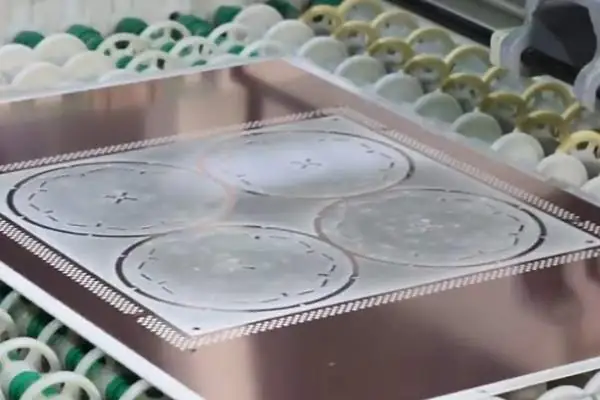
I’ve always found working on network communication PCBs particularly interesting. Every time I see those complex circuit boards eventually become part of a router or switch, I feel a sense of accomplishment. But honestly, this thing looks simple, but it’s anything but.
You need to understand one thing: not all manufacturers can handle the high demands of network communication PCBs. Some manufacturers might be fine for general consumer electronics, but they fall short in the extremely stability-critical field of network equipment. I’ve seen too many projects delayed because of choosing the wrong manufacturer.
The fit between the chip and the PCB is particularly critical. Everyone knows they expand at different rates with temperature changes, but few truly consider this detail during the design phase. Sometimes, choosing cheaper substrates to save costs results in products failing quickly.
I remember one project where neglecting this point led to frequent failures in an entire batch at the customer’s site. Things improved after we switched to a manufacturer specializing in network communication PCBs. They not only selected high-quality materials but also followed network equipment standards in their manufacturing processes.
There are indeed many PCB manufacturers on the market now, but few truly understand network PCBs. This requires considering not only signal transmission quality but also long-term reliability.
Once, we visited a manufacturer’s factory and were surprised to find they strictly controlled the temperature and humidity in the workshop. They explained that this was to ensure the consistency of every board. This attention to detail has truly given me a new understanding of network communication PCB manufacturing.
When choosing partners, my top priority is their attitude towards quality, not just the lowest price. After all, reliability is king in the network equipment field; nobody wants an entire system crashed because of a single board defect, right?
I’ve always found the field of network communication PCBs particularly fascinating. Last year, our team took on a project where a network communication PCB manufacturer sent samples for testing. The samples revealed signal integrity issues at high frequencies.
We spent two weeks repeatedly adjusting the trace layout to resolve the problem. Many issues stem from details; for example, crosstalk between adjacent signal lines is easily overlooked. Once, during testing, I noticed a sudden 30% drop in signal quality on a certain channel. It turned out to be due to a newly added clock line not being properly isolated. This kind of interference is often not immediately apparent but only becomes visible at specific frequencies.
Now, when designing network PCBs, I tend to focus more on the basic architecture. Sometimes, I see colleagues pursuing the latest technologies while neglecting the most basic impedance matching, which can be counterproductive. I recall a case where a client insisted on using ultra-fine linewidths to increase density, resulting in excessive characteristic impedance fluctuations and ultimately necessitating a redesign.
The choice of PCB materials is also quite interesting. We once compared the high-frequency performance of different substrates and found that more expensive materials aren’t necessarily better; the key is the actual application scenario.
Regarding crosstalk, I believe prevention is more important than remediation. In a recent project, I specifically added protective ground lines around critical signals. Although this took more layout time, it significantly saved a lot of trouble during later testing. Such small upfront investments often prevent major problems later.
The deepest lesson I’ve learned in this industry is the importance of combining theoretical knowledge with practical experience. Even the most advanced simulation software cannot replace the subtle issues discovered in actual testing.
Sometimes, the simplest solutions are the most effective. For example, properly planning the number of routing layers can significantly improve signal quality; there’s no need to blindly pursue high-density interconnects.
Now, whenever I see a new PCB design, I first focus on whether its basic architecture is reasonable. Good design is often reflected in these fundamentals rather than the number of advanced features used.
Circuit boards are more than just that green board in a phone
From disassembling old routers to visiting electronics manufacturing plants, I gradually realized
As an electronics enthusiast, I’ve come to understand firsthand the impact of
- Pienten ja keskisuurten erien tuotannon asiantuntija
- Korkean tarkkuuden piirilevyjen valmistus ja automatisoitu kokoonpano
- Luotettava kumppani OEM/ODM elektroniikkaprojekteihin
Aukioloajat: (ma-la) klo 9:00-18:30.