
Heat Dissipation Challenges and Solutions in PCB Circuit Board Design
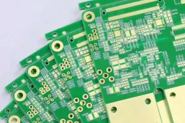
Circuit boards are more than just that green board in a phone
I’ve always felt that many people have a misunderstanding of high-frequency PCBs. They always focus on material parameters, as if choosing a low-loss substrate can solve all problems. In reality, when working with RF circuit boards, I’ve found that the factors that truly affect performance are often the fundamental design details that are easily overlooked.
I remember once debugging an RF PCB for a 5G base station. Even though we used top-of-the-line high-frequency materials, the signal integrity didn’t meet expectations. Later, we discovered the problem was in the power distribution network – the placement of those numerous small capacitors completely ignored the current loops. This made me realize that even the best materials can’t compensate for a poor layout.
Now, when I work with high-frequency PCB manufacturers, I particularly value their understanding of electromagnetic compatibility. Some suppliers can provide RF circuit boards with very stable Dk values, but their design teams can’t even handle basic common-mode noise. Once, during acceptance testing, we found that although individual modules passed testing, the entire board experienced inexplicable clock jitter during operation. Finally, we traced the problem to issues with the grounding methods between different functional modules.
Plane design is especially challenging. I’ve seen too many designs that, in pursuit of wiring density, fragment the power plane into pieces. As a result, in the millimeter-wave frequency band, these cracks become natural sources of electromagnetic radiation. A good designer should handle current paths like planning urban traffic – ensuring smooth main routes while preventing interference between signals of different frequencies. The selection of capacitors is also crucial. Many people think that simply adding a large number of decoupling capacitors will solve the problem, but in high-frequency environments, the ESL and ESR parameters of capacitors are often more important than the capacitance value. We once specifically compared two different packages of 0402 capacitors, and their impedance characteristics differed by more than three times in the 28GHz frequency band.
A high-frequency PCB manufacturer I recently worked with surprised me. They no longer simply emphasized material parameters, but provided complete electromagnetic simulation reports, clearly marking even the impedance discontinuities caused by connector pads. This attention to detail is key to making high-quality RF circuit boards.
Ultimately, high-frequency design is a systems engineering problem. Instead of focusing on a single parameter, it’s better to grasp the overall layout and coordination. It’s like conducting a symphony orchestra; every instrument must play the right note at the right time.
I’ve encountered an interesting phenomenon among many engineer friends working on RF projects – many spend too much time on design software operations and neglect the most basic material selection issues. I remember a team working on a 5G base station project that had to rework an entire batch of boards because they chose the wrong board material – the losses were significant.
RF circuit boards and high-frequency PCBs are far more sensitive to materials than many people realize. Sometimes, switching to a different supplier’s substrate, even if the parameters seem similar, can result in several percentage points difference in actual measured loss. Especially now that equipment is becoming smaller and circuits are becoming finer, the stability of the material itself has become a decisive factor.
A common misconception is that people always focus on high-end process parameters but ignore the most basic issue of copper foil roughness. I’ve seen many cases where even top-tier high-frequency PCB manufacturers were used, but due to improper copper surface treatment, signal integrity was severely compromised. It’s like buying high-quality ingredients but using the wrong cooking method – a real waste.
In fact, there’s a very intuitive way to judge whether a high-frequency PCB manufacturer is reliable – see if they dare to openly compare the production data of different materials. Truly confident suppliers will proactively tell you the loss curves of each material and even provide stability data for different batches of products. This transparency is more effective than any brochure.
Speaking of process details, one easily overlooked point is the treatment of the solder mask layer. Many people think it’s just a protective layer, but in high-frequency environments, the dielectric properties of low-quality ink can directly interfere with signal transmission. During one test, we discovered that simply changing the solder mask ink supplier for the same circuit board material could result in a 0.2 dB/mm difference in insertion loss, a figure that is quite critical in the millimeter-wave frequency band.
Now, some RF PCB suppliers are starting to offer material matching services, which is quite interesting. They no longer simply sell circuit boards, but instead recommend matching copper foil types based on your frequency band requirements, and even adjust the chemical immersion silver plating formula accordingly. This kind of overall solution truly saves customers a lot of trial-and-error costs.
However, it’s important to be wary of being misled by some manufacturers’ claims of “special processes.” In fact, the core manufacturing methods in the industry have long been standardized. The key lies in the precision of execution. For example, with back drilling, some manufacturers can control it within ±0.05mm, while others can’t even guarantee ±0.1mm. These differences in detail often determine the yield rate.
Recently, while helping a friend inspect a batch of antenna boards, we discovered a new problem – some manufacturers, in pursuit of low loss, make the dielectric layer extremely thin, resulting in mismatched thermal expansion coefficients and microcracks after multilayer board lamination. Therefore, when selecting materials, we now prioritize thermal stability more than the loss coefficient, because reliability is paramount.
In fact, from a user’s perspective, instead of focusing on a single parameter, it’s better to look at the manufacturer’s quality control processes, such as how they handle material batch variations and whether they have a complete incoming material inspection system. These seemingly basic things often reflect the true level of quality better than technical specifications.
I recently had a conversation with a friend who works in communication equipment, and we discovered an interesting phenomenon – their team spent more than half a year developing a new product prototype, but the test results were always unstable. Later, they traced the problem to a seemingly ordinary RF circuit board. This reminded me of something many engineers tend to overlook: high-frequency PCB design is actually a systems engineering problem.
Many people think that finding a reliable high-frequency PCB manufacturer is all that’s needed. But the performance of RF circuit boards is often determined by those invisible details – such as uncontrolled dielectric loss caused by improper material selection. I’ve seen people use ordinary FR4 material for designs above 5GHz to save costs, resulting in signal attenuation so severe it’s like trying to hear someone talking through a wall. Impedance matching is far more complex than imagined, especially when dealing with multi-layer boards. Once, we tested a certain antenna module and found that the same circuit layout performed very differently on boards from different batches. Later, we discovered that the lamination process caused a fluctuation of 0.2 in the dielectric constant. This seemingly small change caused the characteristic impedance to deviate from the design value by 8 ohms.
Conductor loss is also often underestimated, especially when frequencies reach the millimeter-wave band. The effect of copper foil surface roughness is amplified exponentially, like racing an F1 car on sandpaper. We conducted comparative experiments, and reducing the copper foil roughness from 5μm to 1μm directly improved insertion loss by 15% at 28GHz.
The most troublesome aspect is that these factors are intertwined. For example, choosing ultra-low-loss materials to reduce dielectric loss often leads to poor thermal conductivity, requiring a reconsideration of the heat dissipation solution. Strengthening the heat dissipation structure, in turn, often introduces new parasitic parameters.
Therefore, when my team and I design high-frequency circuit boards, we focus more on early-stage simulation, especially checking phase consistency at different frequency points. After all, modern communication equipment has increasingly stringent timing requirements; sometimes, a 0.1 ps jitter can cause the entire link to fail.
When choosing an RF PCB supplier, don’t just look at the price list. I pay particular attention to their quality control processes, such as whether they perform dielectric constant sampling on each batch of boards and whether they have dedicated test equipment for the microwave frequency band. These details are often more important than the numbers on the price list.
Ultimately, high-frequency design is like tuning an instrument; it’s not simply about piling on expensive materials to get good sound. It requires finding a balance between loss, impedance, and cost based on the specific application scenario. This is where the true value of an engineer lies.
After working in high-frequency design for a long time, you’ll notice an interesting phenomenon—sometimes, the expensive special materials you buy are less effective than simply doing the basic design well. I’ve seen too many engineers obsessing over the number of decimal places in the Dk value while neglecting the most basic impedance matching. While suppliers claiming to handle millimeter-wave frequencies are indeed impressive, what truly determines the success or failure of a project is often the most ordinary via design. I remember a project team working on automotive radar last year that initially insisted on finding a manufacturer capable of processing ultra-low-loss materials. However, the first batch of samples failed because deviations in the grounding via locations caused complete phase inconsistency. Later, we shifted our approach, focusing on controlling transmission line tolerances, and were able to achieve the required specifications using conventional high-frequency PCB materials. This made me realize that often, so-called technical bottlenecks are actually self-imposed limitations in design thinking.
Now, many chip manufacturers are integrating the RF front-end and antenna directly into the package, which is a challenge for traditional high-frequency circuit board manufacturers, but it also creates new opportunities, such as the design of special carrier boards to accommodate the packaging. A recent project I worked on was attempting to use a carrier board-like process to create a 77GHz radar antenna array, which is more practical than simply pursuing top-tier material specifications.
Speaking of material selection, I don’t think it’s necessary to blindly follow the top-tier specifications. Unless it’s for aerospace applications, medium-loss high-frequency PCBs are perfectly sufficient for most consumer electronics scenarios. The key is to thoroughly understand the intricacies of multilayer design. During a visit to a high-frequency PCB manufacturer’s production line, I found that they could produce power amplifier boards for 5G base stations using modified standard FR4 materials, relying on precise control of copper foil roughness and resin content.
The real headache is thermal management, especially when combining high-power RF boards with high-density packaging. Mismatched thermal expansion coefficients can lead to microcracks. We once learned a lesson from stacking too many blind vias directly under a chip; during high-temperature aging, all the solder balls cracked. Now, when encountering similar situations, we advise clients to leave buffer zones.
Lately, I’ve increasingly felt that this industry is undergoing a bifurcation: one end pursuing ultimate performance for military and aerospace applications, and the other end focusing on cost-sensitive mass-market consumer electronics. As designers, we need to clearly determine which category a project belongs to, rather than trying to force a solution where it doesn’t fit. After all, not all scenarios require radar-level precision.
Every time I see those precision high-frequency PCB boards, I think how interesting they are. Unlike ordinary circuit boards that simply need connected lines to function, in the high-frequency world, signals become incredibly sensitive, even delicate. I remember when I first started working with RF PCBs, I thought that simply drawing the lines correctly was enough. However, the resulting boards had severe signal attenuation. Only later did I understand that the problem was with the material; ordinary FR4 simply couldn’t handle the demands of high-frequency signals. Choosing the right high-frequency circuit board material is a bit like selecting ingredients – freshness determines the final taste. Some manufacturers cut costs by using low-end substrates, resulting in unstable performance across entire batches of boards. Truly reliable high-frequency PCB manufacturers strictly control the materials because they understand this directly impacts signal integrity. I’ve seen cases where the design was flawless, but improper board material selection led to frequent disconnections in the entire communication module.
Many smart devices are now moving towards higher frequencies, placing increasingly stringent demands on the precision of RF circuit boards. Even a slight deviation of a few micrometers in line width can affect impedance matching. When choosing an RF PCB supplier, I prioritize their quality control process. Good manufacturers proactively provide impedance test reports instead of waiting for the customer to ask. Once, our project encountered signal interference issues, and we later discovered it was due to substandard plating processes at the PCB manufacturer, resulting in surface roughness that affected signal transmission.
In fact, the biggest challenge in high-frequency PCB manufacturing is overall collaboration. Design engineers can’t just focus on software simulations; they need to understand material characteristics. Manufacturing engineers also need to understand the design intent. Some excellent high-frequency PCB manufacturers I’ve worked with have technical consultants who get involved in the design phase early on, providing manufacturability suggestions. This integrated approach truly saves a lot of time and effort.
With the popularization of 5G and the Internet of Things, the application scenarios for high-frequency PCBs are becoming increasingly widespread, from base station equipment to smart homes, all utilizing RF technology. However, I think there’s a misconception in the industry: too much emphasis is placed on parameter specifications while neglecting the actual application environment. For example, some automotive radar circuit boards have impressive laboratory data, but their performance fluctuates in environments with significant temperature variations. Good engineering thinking should incorporate environmental factors into the design considerations.
Recently, while working on a smart wearable project, I found that even PCBs with the same frequency require different strategies depending on the product form factor. The RF circuit board in a watch needs to consider flexibility and bending, while the one in a mobile phone needs to consider heat dissipation. These details are often more important than simply pursuing high-frequency parameters. Truly professional high-frequency PCB manufacturers collaborate with R&D teams with an understanding of the application scenario, rather than mechanically producing boards according to specifications.
Sometimes, looking at these tiny circuit boards, the size of a fingernail, capable of carrying gigahertz-level signal transmission, I’m truly amazed by the incredible speed of technological advancement. But the more complex the technology, the more we need to return to the fundamentals: high-frequency PCBs ultimately need to serve specific application needs.
I’ve always felt that many people have a misunderstanding of high-frequency circuit boards. Everyone is always blindly chasing after impressive-sounding material parameters and technical specifications, neglecting the most basic design logic.
I remember last year a client came to me with a design plan, densely annotated with various dielectric constant parameters, even specifying the copper foil thickness to three decimal places. When I asked him why he chose this configuration, he stammered that it was the industry standard practice. In reality, many so-called standard solutions are not suitable for specific projects.
Take RF PCBs, for example. Once we took on a base station project, and the client insisted on using the highest-grade materials for the entire board. However, during testing, we found that the signal quality in certain areas was worse than expected. Later, we replaced the ordinary areas with conventional materials, only retaining high-performance materials in the critical signal paths. This not only reduced costs by 30% but also improved overall performance.
Planar design is also a major problem area. I’ve seen too many engineers fragmenting the ground plane, calling it “interference isolation.” In reality, a discontinuous reference plane is the biggest source of interference. It’s like a highway suddenly having a dead end; the signal energy has nowhere to go and can only reflect everywhere.
The choice of copper foil is even more interesting. Currently, everyone in the industry talks about HVLP copper foil, as if you can’t do high-frequency designs without it. But in my experience, for scenarios below 10GHz, specially treated conventional copper foil is perfectly sufficient. The key is to match the surface roughness to the actual operating frequency, rather than blindly pursuing the highest specifications.
We recently experienced this firsthand in a car radar project. The client initially specified a high-frequency board material from a well-known brand, but through simulation, we found that ordinary FR4 material with a suitable stacking design could meet the requirements. The final board not only passed all tests but also cost 40% less than the budget.
I think the biggest taboo in high-frequency PCB design is dogmatism.
Each project has unique application scenarios and constraints. Instead of blindly applying theoretical formulas from textbooks, it’s better to calmly analyze the actual needs.
For example, when we helped a telecommunications company redesign their system, we found that the expensive high-frequency circuit boards they purchased were only performing at 60% of their potential. By adjusting the dielectric thickness distribution, we achieved better impedance control with a more economical combination of materials. Sometimes, the key to solving a problem isn’t the material itself, but how to effectively utilize existing resources.
Ultimately, high-frequency circuit board design is more like a balancing act. Finding the optimal balance between performance, cost, and manufacturing feasibility requires designers to have a deep understanding of every aspect.
Many young engineers today rely too heavily on simulation software, constantly running full-wave analyses. In reality, some fundamental problems can be solved with simple empirical judgment. Just like a doctor can’t rely solely on CT scans to diagnose a patient, they also need to use observation, listening, questioning, and palpation. For instance, observing the distribution pattern of resonance points can quickly identify power integrity issues; or measuring small fluctuations on the TDR curve can pinpoint the location of impedance discontinuities. These practical techniques are often more effective than complex simulations in quickly identifying the root cause of a problem.
I firmly believe that good design isn’t about using the most expensive materials, but about solving practical problems with the most suitable solutions. For example, in the millimeter-wave frequency band, the stability of the substrate’s dielectric constant is more important than its absolute value; and in high-power applications, thermal management capabilities are often more critical than dielectric loss. Designers need to be like chefs, carefully selecting and combining materials based on different application scenarios.
This industry is constantly evolving, with new materials and technologies emerging all the time. From low-loss PTFE to hydrocarbon ceramic-filled materials, from hybrid lamination techniques to embedded passive components, each innovation brings new design possibilities. But truly excellent designers know how to make wise choices between new technologies and mature processes.
However, some fundamental principles will never become obsolete: understanding the underlying physics, focusing on practical applications, and maintaining an open mind. For example, the propagation laws of electromagnetic waves in dielectric materials and the mechanisms of the skin effect are fundamental physical principles that remain the foundation of design, regardless of technological advancements. At the same time, it’s crucial to pay close attention to the realities of manufacturing processes to avoid designing “paper circuits” that cannot be mass-produced.
After all, we are designing not just parameters, but products that actually work. A circuit board that performs perfectly in laboratory tests but fails to withstand real-world temperature variations, mechanical vibrations, and long-term aging is ultimately a failed design. The true value lies in ensuring the circuit board operates stably and reliably in the final product for years, even decades.
When dealing with high-frequency PCB design, I’ve found that many people focus excessively on theoretical parameters while neglecting practical application scenarios. Once, when designing an RF circuit board, we overly pursued a perfect ground plane structure, only to discover unexpected resonance problems during actual testing.
The most troublesome aspect of high-frequency circuit boards is signal integrity. I remember a project where we used materials from a top-tier high-frequency PCB manufacturer; the theoretical loss parameters were excellent, but in actual application, we encountered serious signal attenuation. Later, we realized it was because we relied too heavily on the ideal data provided by the simulation software.
When choosing an RF PCB supplier, I value their practical case experience more than their technical specifications. One supplier provided samples that performed only moderately well in laboratory tests; but another smaller manufacturer offered a more practical solution.
The biggest misconception in RF circuit board design is over-reliance on simulation. Simulation software can indeed help us predict many problems, but it can never fully simulate the complex interference in a real-world environment. I once encountered a case where the simulation results showed a perfect design; but during actual testing, a tiny impedance mismatch caused the performance of the entire board to degrade.
The most easily overlooked problem in high-frequency PCB design is thermal management. As the frequency increases, the heat generated by dielectric loss significantly affects material performance; I once saw a design that performed excellently at room temperature, but the signal quality deteriorated sharply at high temperatures. Good high-frequency PCB manufacturers provide detailed material temperature characteristic curves, and this data is often more valuable than simple loss parameters.
In fact, the most practical experience often comes from failures; once, to reduce loss, we chose an ultra-thin dielectric, but during the production phase, we found the yield rate was extremely low; ultimately, we had to redesign it; this made me realize that sometimes moderate loss is more reliable than pursuing perfection.
Modern RF circuit board design increasingly requires balancing multiple factors; simply pursuing low loss or perfect impedance matching may lead to other problems; a truly excellent design finds the optimal balance under various constraints.
I recently had a conversation with a friend who works in communication equipment, and I discovered an interesting phenomenon. Their team spent over half a year developing a new product prototype, but during testing, they consistently encountered signal drift problems. After extensive investigation, they discovered the issue stemmed from using ordinary FR4 circuit boards, which experienced dielectric loss in the high-frequency environment. This case made me realize again how crucial the selection of appropriate high-frequency PCBs is to overall system performance.
Many people mistakenly consider RF circuit boards simply an upgraded version of ordinary circuit boards. In reality, when signal frequencies exceed the GHz threshold, the situation changes completely. It’s like a highway suddenly turning into a winding mountain road, requiring more specialized driving skills. At this point, the dielectric constant stability of the circuit board directly affects the phase consistency of signal transmission. I’ve seen many project teams choose ordinary materials in the prototyping stage to save costs, only to end up with complete rework.
I remember visiting a manufacturer specializing in high-frequency PCB manufacturing last year. Their workshop temperature was consistently controlled within a range of ±0.5 degrees Celsius. This extreme requirement for the production environment precisely illustrates that high-frequency circuit board manufacturing is not simply a matter of stacking processes, but requires systematic control. Especially when it comes to multi-layer board lamination, the matching of thermal expansion coefficients of different materials directly affects the reliability of the final product.
Interestingly, even traditional industrial products like automotive radar are now facing high-frequency challenges. Millimeter-wave radar RF PCBs need to consider not only signal integrity but also the effects of vibration and sudden temperature changes. This reminds me of a supplier who mentioned that the high-frequency circuit boards they customized for an autonomous driving project needed to undergo 200 thermal cycling tests to be considered qualified.
When choosing a reliable high-frequency PCB supplier, I value their ability to solve unconventional problems more than anything else. For example, we once needed to achieve a continuously varying impedance design within a limited space. The solution provided by our partner was to use mixed dielectric materials in a specific layer. This kind of flexible problem-solving ability is far more convincing than simply showcasing certification certificates.
In fact, observing how a manufacturer handles details reveals their level of professionalism. For example, the high-frequency PCB manufacturer we recently collaborated with even performs three inspections on the chamfer angle of the gold fingers. This kind of obsession with precision is necessary in the high-frequency field. After all, when the signal wavelength approaches the trace size, any tiny imperfection will be magnified.
With the widespread adoption of 5G and IoT devices, I believe that more industries will face the challenges of high-frequency design in the future. This is not just a technological upgrade, but a complete shift in design thinking, moving from pursuing connectivity to managing electromagnetic compatibility. Perhaps this is the new normal that engineers need to adapt to.
I’ve seen many engineers stumble in high-frequency PCB design—they always treat material parameter tables as sacred texts. In reality, those Df values and Tg temperatures are just basic thresholds. What truly determines the success or failure of an RF circuit board is often what’s not written in those data sheets.
Take our 5G base station project from last year, for example. We chose a material from a supposedly professional high-frequency PCB manufacturer, and the Df values in their datasheet looked excellent. However, when the first batch of boards arrived, we found that the phase noise was excessive. We later discovered that unstable pressure control during lamination caused the dielectric thickness to fluctuate by three thousandths of a millimeter. This micron-level error directly ruined the performance of the entire antenna array.
The biggest enemy of high-frequency circuit boards is idealized thinking. Do you think calculating the dielectric constant to four decimal places is enough? In actual prototyping, the moisture absorption rate of the board material, the roughness of the copper foil, and even the dielectric properties of the solder mask ink can all cause problems. I know a team that works on military radar; when choosing RF PCB suppliers, they deliberately test at twice the design frequency—only materials that maintain stability under extreme conditions are used in their products.
Once, I visited a Japanese high-frequency PCB manufacturer. Their quality control workshop was kept at an extremely precise constant temperature and humidity; even the operators had to wear anti-static clothing and pass through three air showers. At first, I thought they were overdoing it, but then I saw them using a laser rangefinder to measure the Z-axis expansion coefficient of each board, and I realized that the reliability of RF circuit boards is truly supported by these details.
Many people are now struggling with upgrading FR series materials. Instead of blindly pursuing higher Tg temperatures, it’s better to first thoroughly understand the limitations of existing materials. We tested the same FR substrate, and the loss difference between different manufacturers at below 1GHz could be more than double. Some high-frequency PCB manufacturers adjust the weaving angle of the fiberglass cloth by a few degrees; this seemingly insignificant change actually has a crucial impact on phase consistency. Truly reliable high-frequency PCB design is like woodworking – you need to understand the characteristics of each material and leave room for potential deformation. Those parameter tables are merely an entry ticket.
I’ve seen many engineers get overly fixated on the numbers in material parameter tables when choosing high-frequency PCBs. In reality, what truly determines the success or failure of an RF circuit board is often not the top-of-the-line substrate material, but rather the meticulous control of details during the manufacturing process.
I remember a project last year involving base station antennas. The client specified a high-end board material from a particular brand. The supplier they chose offered a lower price, but their lamination process was unstable, resulting in dielectric constant fluctuations exceeding 5%. Later, they switched to a high-frequency PCB manufacturer that emphasized process control, and with the same batch of materials, the performance stability improved significantly.
Many RF PCB suppliers now like to advertise the number of imported testing equipment they own, but what’s truly important is whether they have established a complete measurement process. For example, one factory we collaborated with didn’t just perform random TDR impedance testing; they measured every critical trace on every board and included a comparison curve of the measured data against the design values in the factory report. This dedication to reliability is far more valuable than simply looking at an equipment list.
High-temperature and high-humidity testing is now basically standard practice in the industry, but what truly tests the technical strength of a high-frequency circuit board manufacturer is their ability to maintain performance under extreme conditions. We once simulated the low-temperature environment of an Arctic station and found that some materials claiming ultra-low loss showed significant degradation in phase stability at -40 degrees Celsius. This reminded us that we can’t just rely on room-temperature parameters.
In the future, with the development of terahertz technology, the boundaries of traditional PCB materials will be constantly pushed, but I think what’s more urgent is improving the precision ceiling of existing processes. For example, what is the interlayer alignment accuracy of multilayer RF boards now? This might have a more significant impact on insertion loss in the millimeter-wave band than switching to new materials.
Sometimes I wonder if the industry is overly focused on new materials and neglecting the fundamental aspects of manufacturing. After all, even the best design concepts ultimately depend on the high-frequency PCB manufacturing process. Instead of chasing after substrates with more impressive parameters, it might be more practical to first ensure that existing processes can fully utilize the potential of ordinary materials.
Circuit boards are more than just that green board in a phone
From disassembling old routers to visiting electronics manufacturing plants, I gradually realized
As an electronics enthusiast, I’ve come to understand firsthand the impact of
- Pienten ja keskisuurten erien tuotannon asiantuntija
- Korkean tarkkuuden piirilevyjen valmistus ja automatisoitu kokoonpano
- Luotettava kumppani OEM/ODM elektroniikkaprojekteihin
Aukioloajat: (ma-la) klo 9:00-18:30.