

Head-Up Display PCB Design: Thermal, High-Speed and Heavy Copper Trade-Offs for TFT, DLP and LBS HUDs
After nearly ten years and more than twenty HUD PCBs, I found
Some time ago a project gave me quite a headache: the I/O modules of the DCS on site dropped signals every now and then, and after checking back and forth, I found that the redundant switching circuit on the board was simply not synchronized with the operating rhythm. This made me reconsider a question: have we deified the word redundancy already at the PCB stage? Many system integrator friends, as soon as the DCS PCB comes up, start by demanding dual redundancy, hot swap and hardware voting, as if keeping a spare channel settles everything. But I increasingly feel that for a Distributed Control System PCB that has already gone to multilayer boards, heavy copper and high-density routing, redundancy is more like a double-edged sword: it preserves availability but quietly gnaws away signal determinism in places you cannot see.
Take the power switching part. To let I/O modules be plugged and unplugged live, soft start and isolation must be built separately on that four-layer or six-layer board, and heavy copper is usually needed to carry the instantaneous large current. In earlier years we always went to one fixed multilayer pcb supplier for this, whose conventional multilayer board process was very stable, but once local 4 ounce or even 6 ounce copper thickness Heavy copper PCB requirements were met, delivery began to float. Once, in a board we got, the etch factor at the copper edge of the power plane had not been controlled well, making the equivalent resistance of the switching loop higher than the design value by a margin, and as a result, during hot swap the surge blew the fuse at the front end. At that time I realized that finding a manufacturer that truly understands the heavy copper process is far more important than adding several more redundant paths in the circuit. Unfortunately many peers, when selecting, stare only at layer count and line width and spacing in the quotation of the multilayer pcb manufacturer and overlook that thick copper is not on the same order of magnitude as ordinary FR-4 in Z-axis expansion rate.
The bus interface side is an even harder-hit area. For the isolation of HART or fieldbus signals, in essence the same differential pair has to carry both a digital heartbeat and superimposed analog disturbance. At the PCB level this is no longer a question of how many layers, but of how delicate the stackup and return path are. I once modified a DCS main control backplane, originally an eight-layer board, in which the power layer and ground layer were too close together, and parasitic capacitance ate part of the modulated signal edge, causing devices on the intrinsically safe side to fail handshake occasionally. Later I switched to another multilayer pcb supplier, who suggested running two inner-layer signals sandwiched between a pair of same-polarity reference layers, so that the return path for high-frequency components was cleaner. After the change, the bit error rate of the whole station dropped visibly to the naked eye, but do you say this had anything to do with redundancy? No direct relation. Yet the stability users finally feel happens to grow out of these non-redundancy details.
There is another place particularly easy to overlook, which is the thermal cycling life of heavy copper boards. The ambient temperature in a DCS cabinet is not as constant as in an IT machine room, and in summer, cards near furnaces may stay for a long time in a mild baking state of fifty or sixty degrees. If an ordinary heavy copper pcb manufacturer uses a high-Tg but low-toughness resin system, after three or four years the bonding force between the copper layer and the substrate begins to decay. The most outrageous case I have seen was a redundant main control card at a petrochemical site that suddenly went offline, and when it was pulled out, it was not that the chip had burned but that the power copper foil, after many thermal expansions and contractions, had lifted as a whole sheet from the root of the pad. After that, when choosing a heavy copper pcb supplier again, the first thing I asked was not how many ounces you can make but whether your thick copper boards have been through thermal shock validation of more than 500 cycles.
Ultimately, hardware like DCS that runs ten years without rest needs not a design declaration of several redundancies on paper but repeatability of every lamination and every etching on the production line. A redundant circuit can be drawn extremely elegantly in the schematic, but if your multilayer pcb manufacturer cannot even keep the alignment accuracy of inner layers from floating around, the backup channel may instead become a hidden interference source. My habit now is to lower the key of redundancy a bit at the system design stage and pour energy into seemingly clumsy things like board material, copper thickness uniformity and drilling quality. The longer I do hardware, the more I feel that a DCS PCB that is honest, with no cold solder and no interlayer shorts, lets one sleep more soundly than a hundred pages of redundancy analysis report.
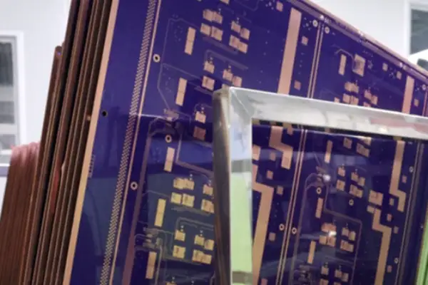
I used to always feel that DCS hardware had no mysticism, that having drawn several four-layer boards and used isolated power supplies would settle it, until an offshore platform project completely changed my view. At that time, because of space limits, we had to stuff the redundant controllers and I/O links of the whole distributed control system onto one 12-layer board, and after finding several multilayer board manufacturers for prototyping, problems were exposed as soon as power was applied: not that the routing did not connect, but that redundancy and hot swap had been understood as paper labels, and almost paralyzed the entire bus system during live maintenance.
On that DCS PCB, we piled up two sets of fully symmetric computing cores, thinking hardware voting could achieve gapless switching. The result was that, without pinning down the copper thickness and impedance control of the power layer at a thick copper PCB manufacturer of the same batch, the reference grounds of the two redundant boards would fight under transient current of several dozen amps, jumping between primary and backup, not at all nanosecond-level synchronization but pulling several dozen milliseconds of glitches directly on the bus arbiter. Later we honestly found a factory that specialized as a heavy copper PCB supplier, pulled two power copper layers in the six-layer stackup to 5 ounces, and also buried TVS clamps and soft-start hot-swap controllers near the gold fingers of each plug-in card, and only then absorbed the surge current and common-mode noise at the instant of insertion and removal. The fieldbus part was even more of a headache: Modbus and CAN H run mixed with 4-20mA loops, cable lengths often over a hundred meters, and if the multilayer board supplier does not know how to sandwich split-ground isolation between layers and precisely control differential pair spacing, HART signals directly punch the analog readings to pieces.
My basic judgment of DCS hardware now is: what you choose is not a multilayer board manufacturer but the fault tolerance bottom line of your site. Hot swap is never for the convenience of replacing cards but the only chance of online repair, and redundancy cannot be patched together by duplicate devices either: it needs the physical layer of the entire power distribution network and bus to bury an escape route for single-point failure in advance. With these lessons, whenever I audit the stackup report of a heavy copper PCB manufacturer, I stare tightly at board thickness uniformity and current-carrying capability, because I know that thermal fatigue of any pad can, in some unknowing live replacement, become the starting point of the whole system’s shutdown.
After so many years in process control, I increasingly feel that redundancy in the end must show its true colors on the backplane. However lively the primary-backup switchover and voting logic of a DCS is made, as long as the physical isolation of the Distributed Control System PCB behind it is not thorough, it gives you a taste of its colors at the critical moment. A few years ago we met a case where two redundant controllers synchronized through the backplane, and the previous revision used an ordinary multilayer board, with heartbeat constantly lost, and on checking, ground bounce had pulled the common-mode voltage of the synchronization link off. Later we switched to a multilayer board supplier specializing in power management boards, changed four layers to six, and separately allocated a fully shielded layer for peer communication, which finally stopped the jitter of primary-backup synchronization. That board also carried a power redundancy OR-ing circuit, with two 48V busbars from top to bottom having to carry 30 amps continuously, and ordinary 1 ounce copper could not take the heat. We specially found a heavy copper PCB manufacturer, with inner layers directly 4 ounce copper and outer layers 2 ounce, and running full current for three days, temperature rise was only about twenty degrees, so that channels were truly independent.
The voting circuit was even more elaborate: the hardware redundancy switch in the FPGA uses differential signal voting, and even a nanosecond-level disturbance can trigger a false switch, all depending on how accurately differential trace impedance can be controlled. So later we fixed on one multilayer board manufacturer and did not let it change, who could guarantee plus or minus 5 percent impedance tolerance, with line width spacing and normal-temperature drift all calculated clearly. There is another hidden place: the surge path when the primary and backup controllers are hot-swapped, and if the backplane heavy copper is not laid well, the ground potential floating at the instant of insertion can reset the backup machine’s logic, and troubleshooting this kind of fault can make one lose a layer of skin. Later, on new systems, when selecting a multilayer board supplier, I simply had the PCB factory mark the glue flow quantity and prepreg model of every layer on the stackup drawing, and without even one of these, I would not sign the sample.
In the end, redundancy is not piled up by protocols but rammed in micron by micron with copper thickness, stackup and isolation. Those heavy copper PCB suppliers that are truly useful will not just quote you an ounce count, but knead current density, heat dissipation path and mechanical stress together into the stackup simulation, and when a board like that is installed in the back frame, when the primary and backup switch over, you will not hear the sound of relays jumping back and forth.
The longer you do industrial control, the more you feel that what is most easily overlooked is instead the board that carries everything. Many people talk about redundancy and hot swap, opening their mouths with protocols and logic, but once it lands on the physical layer, for those high-speed signals and high-current paths running on a Distributed Control System PCB, slight mishandling puts the reliability of the whole system in doubt. I once took part in a project where I/O modules sporadically restarted on site, and after two months checking code, I finally found the DCS PCB stackup had not been laminated well, and the resonance point of the power plane happened to fall in the switching noise band, and changing to another multilayer pcb manufacturer for re-prototyping made the problem disappear directly. Since then I no longer superstitiously believe in the original manufacturer’s reference design but force myself to thoroughly understand the board factory’s process capability.
The trouble brought by modular design is more than imagined. We always think that splitting functions into independent plug-in units settles everything, but in fact once a card is inserted into the backplane, the return paths of power, ground and signal all change. Especially during live insertion, millisecond-level differences in connector pin contact create ground bounce, and once this ground bounce couples into the control logic of the switching circuit, the switching action may be falsely triggered. Many people put attention on the symmetry of signal length matching, but I feel what deserves more attention is the collapse of the power rail at the switching instant. In my design I simply made a separate supply for the voting and switching part, taken directly from the backplane’s redundant power, isolated with Heavy copper PCB traces and ferrite beads, and not sharing wet connections with the VCC of any microcontroller. Facts proved that even if the main control module loses power, the switching logic does not move at all.
Speaking of Heavy copper PCB, in fact the factories in China that can make thick copper boards well are just a few, and when looking for a Heavy copper PCB supplier you really cannot look only at website promotion. I once used a factory claiming it could make 10oz copper thickness, and the prototype that came out had serious inner-layer copper blistering, and delivery was also delayed by half a month. Later I switched to a Heavy copper PCB manufacturer specializing in heavy power boards, who used multiple laminations plus laser drilling to bring the temperature rise of the high-current module down to an acceptable level. In an industrial site, cabinet temperature in summer easily goes to 60 degrees C, and if the power module in a DCS rack relies on ordinary copper-thickness traces, IR drop makes voltage fall outside the error range, and then neither redundancy nor switching helps.
In choosing a multilayer pcb supplier, what I value is not how many layers they can make but the transparency of impedance control and material library. Many unbranded board factories use cores and prepregs from small domestic factories, with extremely large batch fluctuation of dielectric constant, and the result is that the impedance of differential pairs floats outrageously. Once clocks and control signals reflect seriously, timing margin at switching is eaten up. Later I fixed on one multilayer pcb manufacturer, who directly provided measured data of Rogers and Taiyao board materials and had strict process specifications for keep-out zones and back-drilled stub control. You may not believe it, but just by changing the board factory, the bit error rate of the system bus dropped by two orders of magnitude.
A few more words about power. Many people, when drawing a Distributed Control System PCB, like to connect the feedback points of all power modules close to the module outputs. This looks fine, but with long-distance backplane power supply, the actual voltage received by remote I/O modules is lower. My approach is to design a Kelvin sampling point at the far end of the backplane, using a differential line to pull voltage feedback back to the compensation pin of the power module, which is equivalent to making the power output voltage truly stable only at the load end. This change requires running an extra pair of thin lines on the multilayer pcb, but the benefit is that voltage overshoot at the switching instant can be quickly pulled in by the loop, with no inexplicable restarts.
Switching itself is also not that mysterious. I do not pursue microsecond-level handover of control, and for the inertia of an industrial process, a few milliseconds faster or slower simply does not matter. What is really tricky is the open-circuit state during switching: if path A is turned off before path B is fully on, the I/O output drops instantly to an indeterminate level, and the actuator on site may jitter once. So on the DCS PCB I made a make-before-break hardware logic, using a P-channel MOSFET and a capacitor for a simple delay, ensuring that the two control paths are both valid for a short time.
After doing industrial control for a long time, one deeply felt lesson is that those redundancy architectures and hot-swap designs that look high-end are in the end, when landed physically, nothing more than a reliable Distributed Control System PCB. However much time you spend pondering protocols and controllers, if the PCB itself deforms under repeated insertion, pins oxidize, or the current-carrying capacity of the power layer lets you down, the whole module is armchair strategizing.
I remember a project in which, to achieve true hot swap for the DCS I/O modules, we agonized for a long time over pin definitions and long and short pin coordination. But what finally held up progress was instead not finding a suitable multilayer pcb manufacturer. At that time the design required an 8-layer board with two thick copper layers sandwiched inside, which had to carry the inrush current at module startup. An ordinary multilayer pcb supplier shook its head directly on seeing the thick copper and inner-layer heat dissipation requirement, saying yield could not be guaranteed. Later we turned to ask a factory specializing in Heavy copper PCB, who did take the order, but when the prototype came back, the copper around those high-current hot-swap pins had blistered during reflow. This made us thoroughly understand that when designing a DCS PCB you cannot look only at logic, and you must run in with the manufacturing end in advance. Especially when a module has to be pulled out and plugged back in during operation, the mechanical stress of each insertion on pin solder joints and the pulling on the PCB’s Z-axis expansion are simply something an ordinary consumer electronics board cannot withstand. A good Heavy copper PCB manufacturer will discuss with you copper thickness distribution and the choice of glass transition temperature point and may even suggest additional copper-plated fill at pin through holes, and these details are far more practical than your calculating current limit slope on the datasheet.
Later we simply split the risk control of hot swap into two blocks: the power logic at the system level and the board reliability at the physical layer, each taking half the weight. In looking for suppliers I would rather spend more time validating their multilayer pcb process and go to the workshop to see their parameters when pressing thick copper cores, than be cheap at the selection stage. Because once a DCS module breaks on site, even the lead seal may be torn off by the user, and you do not even get a chance to explain. In the end, behind every pin marked as supporting hot swap, there must be a board that can withstand countless mechanical shocks and current shocks, and this is the hardest bone buried deepest.
We recently did a project and were stuck by an old problem: how to squeeze HART communication onto a board that already has isolation, without letting analog signal accuracy fall. The topic is rather fine, but I think many hardware peers may have stepped in similar pits.
In the DCS systems I come into contact with, bus isolation on the backplane is in fact not new. Between every slot and the shared bus there is a bus switch or buffer for isolation, and when a module is pulled out of the board, the corresponding bus interface goes directly to high impedance, and backplane communication is completely unaffected. This holds for conventional digital buses, but once you start to consider superimposing HART on 4-20mA, the logic of the whole physical layer has to be sorted out again.
Many people think HART is just simply riding a signal on a current loop, but in fact the water here is deep. The physical layer of HART superimposes an FSK on the 4-20mA DC signal, with logic 1 corresponding to 1200Hz and logic 0 to 2200Hz, with amplitude about plus or minus 0.5mA. The problem is that the output channel of the DCS PCB you make has to do two things at once: precisely output DC current on one hand, and transparently transmit and receive the HART signal superimposed on it on the other, without the two fighting. I have seen quite a few schemes in which problems appear at the place of signal shaping and superposition, and the analog accuracy of 10 microamps simply drifts. This is not something solved by swapping an op-amp or tuning an RC, and the two domains must be completely separated from the architecture.
The structure we use now puts the HART shaping module and the analog output signal conditioning module on a daughter card, leaving isolation and control on the main card. The benefit of this is that they are separated physically, avoiding the trouble of digital ground and analog ground coupling, and when prototyping with a reliable multilayer pcb manufacturer, the control of impedance and interlayer coupling is also much more stable. Especially in making a four-layer stackup, how the power layer and signal layer are arranged directly decides whether the signal integrity of the HART superposition point can be kept. Once we tried integrating the shaping part also into the main card, and the result was that in the 8-channel dense output version, crosstalk between channels was obvious and analog output ripple directly doubled.
There is also an easily overlooked point here, the isolation barrier. If you are only running an ordinary 4-20mA output, doing isolation well depends mainly on creepage distance and insulation withstand voltage. But a HART signal is an AC quantity superimposed on DC, and the high-frequency response of the isolation device directly affects the demodulation bit error rate of FSK. We used several digital isolators to replace optocouplers, with no problem in DC characteristics, but group delay inconsistency in the high-frequency range caused an abnormally high HART modem handshake failure rate. Later we were forced to reselect the heavy copper pcb supplier, because the copper thickness of high-current output channels directly affects heat dissipation and impedance uniformity, and if you do not do this end right, after the board heats up, the amplitude consistency of HART all runs off.
Honestly, my requirements for a heavy copper pcb manufacturer are much stricter now than before. Before, 2oz copper carrying two or three amps felt like nothing, but now with 4-20mA output plus HART, you also have to consider the voltage drop at the field-side terminals, and thicker copper means lower impedance but also a greater test of process flatness and lamination stress. When communicating with a multilayer pcb supplier, you have to tell him clearly which layers carry large current and which carry small-signal superposition, otherwise if he goes by the ordinary process, the board comes back and you feel puzzled even measuring the impedance deviation.
Between modules and the bus, I now prefer an isolated backplane bus architecture, letting the physical layer of every channel be completely independent. When a module is pulled out, the bus enters high impedance, which is basic, but what is truly valuable is that isolation is done thoroughly, so that even if a certain channel has a problem when superimposing HART, it will not interfere with other analog outputs in the whole rack. This is especially obvious when making a high-density DCS rack: in a 48-channel rack, if the impedance of the HART superposition point of one channel changes and couples through the power bus, the HART demodulation success rate of other channels can be pulled down by several percentage points.
Many people doing industrial control do not mention the debugging details of the HART interface, but these things are really ground out bit by bit in actual combat. On the board, impedance matching, capacitive load at the superposition point and group delay characteristics of isolation devices, if any one is not handled well, on site they turn into communication that comes and goes or analog output accuracy exceeding the limit.
In my first few years in industrial control, I always felt that a circuit board was just that, and that finding a multilayer board manufacturer and throwing over the Gerber would be done. Later, after tumbling on several DCS projects in a row, I realized that a DCS PCB simply cannot be covered by the standard of a general PCB. Especially for boards with DP communication and analog acquisition, once routing density goes up, the process deviation of an ordinary multilayer board supplier begins to be exposed, impedance mismatch of differential pairs makes 12Mbps unstable, and stations drop on site from time to time without you being able to find the cause.
Many people think making hardware for a Distributed Control System is just piling up components, but what is actually most headache-inducing is finding a supplier who truly understands heavy copper. A DCS backplane or power distribution layer often has to pass a dozen-plus amps of current, and an ordinary multilayer board manufacturer tells you that doing 2oz copper counts as heavy copper, and when you ask whether 4oz inner layers can be made, the other side begins to hem and haw and double the quote. The Heavy copper PCB supplier I later fixed on to cooperate with said straight out that for inner-layer etching control above 4oz, few have truly long-term production line experience, and many factories subcontract after taking orders, with yield a mess. The worst case I have seen was an outer layer copper thickness nominally 4oz, but the cross-section showed uneven plating, with some places not even reaching 3oz, and this kind of board, sent to run the thermal cycling test for SIL2 certification, cracked directly.
Now the DP interface. In my early days, to save trouble when drawing boards, I routed the A/B lines of RS-485 with a bit of detour and drilled two more rows of vias, and when the DP master on site pulled a long line, the bit error rate at high speed shot up directly. Later I learned my lesson, honestly wrapping ground beside the DP differential pair and making the termination resistor pads deliberately a bit longer, to make it convenient to change resistor values to match the topology on site. These small moves are not something the Heavy copper PCB manufacturer cares about at all: you have to mark clearly that the area under the common-mode choke needs to be hollowed out, and also urge the multilayer board manufacturer not to touch your stackup structure, otherwise they secretly change the prepreg thickness for you and the characteristic impedance floats.
Now when I look back at DCS PCBs drawn by others, my first look is at power layer copper thickness and interlayer coupling of signal layers, my second look is at the length matching of DP traces, and my third is to find that multilayer board supplier’s process capability statement. Many factories that make fast boards dare to take orders, but those who can truly make stable a board like a DCS that is mixed-signal, with safety isolation, and also has to withstand SIL2/3 life requirements are just a few. Do not ask me how I know: a person who has scrapped several hundred boards, on seeing the quotation sheet of a Heavy copper PCB supplier, first turns to the process capability page to see whether they have really made 4oz buried and blind via boards with more than 6 layers. In this matter, the pits for saving money are all waiting for you in the places you cannot see.
I remember a period when our team was working on a chemical plant renovation, and the control system had to be upgraded to a DCS with safety interlock. Every day we dealt with all kinds of drawings, and what turned in my head was always the same thing: how could a seemingly ordinary board withstand the diagnostic coverage required by SIL2 certification? It is not enough to write the program more rigorously, and this matter falls entirely on the hardware.
Once, chatting with a long-cooperating multilayer pcb manufacturer, they were skilled at communication backplanes, but when they heard we wanted a Distributed Control System PCB dedicated to safety loops, their engineering chief shook his head directly, saying that the copper thickness on your board has to be changed, trace spacing has to be recalculated, and power layer splitting is much more complex than usual. I fully understood what he said, because next to safety-related signals are ordinary control signals, and how to cut them physically is simply not something solved by drawing a line.
Later we switched to a Heavy copper PCB supplier specializing in industrial power and heavy copper boards, whose stackup advice was very direct: pull independent copper for the power supply of the safety channel, borrowing no return from general layers all the way from the input terminal to the relay driver. In this way a single-point fault does not easily pass through, and the diagnostic path also becomes much clearer. Of course cost goes up a notch, but that feeling that when a problem occurs it will not be muddled is worth more than the money saved.
Many people think SIL levels are posted by certification certificates. The more I see, the more I feel it is a very paranoid habit in PCB design. Like a Digital Output module we later met, to meet diagnostic requirements, each output not only had to measure current but also loop resistance and short-circuit state, and in the end this diagnostic information could not be hidden away but had to go over an independent channel to the safety logic solver. This requires the board layout to physically separate diagnostic traces from safety signal traces from the very beginning while preventing cross interference, and every step tests the board factory’s control of impedance and spacing.
Speaking of isolation, fiber is indeed a good thing, and later we simply ran all data exchange between the safety controller and the general controller over optical ports. This is not only to satisfy the sentence about electrical isolation in the standard, but because we really met several cases where, when a big pump on site started, communication on copper cable dropped packets, and after a week of checking, it was found that ground plane noise had coupled over. If that was a signal on a safety loop having this kind of problem, I estimate I would not sleep soundly.
The most unforgettable, though, was working with a multilayer pcb supplier on a hybrid laminated board. One side of the board was ordinary FR4 for logic processing, and the other side used high-Tg board material running Heavy copper, specifically to withstand the high temperature and high current of relay switching. For this scheme they at first feared yield would not be good, and after trying batch after batch, they slowly figured out the lamination parameters. Thinking back now, for a DCS PCB, especially a product with a safety loop, design specifications alone are far from enough, and you have to find a board factory willing to tinker with you, who must truly digest which traces on your board are the deadly ones and which can be compromised. Once this tacit understanding is established, afterward, with diagnostics and SIL2 validation, you have much more confidence.
I have come into contact with many industrial control projects and slowly realized something overlooked by many: what decides the long-term stability of a DCS system is often not the controller redundancy or software diagnostics displayed on the surface but the circuit boards themselves hidden in the cabinet. Especially for a Distributed Control System PCB, many integrators stare only at parameters like I/O point count and scan cycle and rarely put thought into what the PCB’s lamination structure and copper thickness actually mean. For power distribution boards and analog acquisition boards, once current is slightly larger and heat dissipation design cannot keep up, the first to collapse are the power rails using ordinary PCB, with a voltage offset of a few tenths of a volt starting to make the acquisition of the whole channel drift, which is especially fatal in a continuously running petrochemical site.
So whenever I handle any project involving DCS hardware now, I clarify one thing from the start: I must find a multilayer pcb manufacturer that truly understands industrial electronics reliability, and not just an ordinary supplier who only presses four-layer boards. What you need is a multilayer pcb supplier who can argue clearly with you about underlying details such as the glass transition temperature of FR4, the porosity of through-hole copper filling and copper foil ductility. For example, even for the same six-layer board, the lamination order and the choice of prepreg can make the board’s Z-axis expansion differ by several times under temperature change, which directly affects the long-term life of BGA device solder joints.
Another unavoidable topic is heavy copper. Many DCS relay output boards or power interface boards may carry a continuous operating current of only two amps, but at a short circuit or surge on site, instantaneous current can soar to several dozen amps. At this time a reliable Heavy copper PCB manufacturer will make copper thickness 4oz or even 6oz and use through-hole plating to ensure sidewall connection, rather than simply using thick copper to photoplot a few thick traces. I remember once replacing a batch of I/O boards in an old system: after changing the original standard copper boards to 3oz thick copper boards made by a Heavy copper PCB supplier, board burn-outs caused by field wiring short circuits almost vanished. This is not mysticism, just copper thick enough and the heat dissipation path wide enough that heat was conducted away before it had time to damage the copper layer.
Finally, I must talk about validation. Many people think running a 72-hour aging before factory shipment counts as validation, but that is only the most basic link. Real PCB-level validation has to be traced back to the bare board stage with flying probe testing, impedance TDR testing, and board-level thermal stress screening. Some process engineers from wafer fabs I cooperate with even require microsections of multilayer boards to check the copper thickness uniformity of through-hole walls, because a micro crack invisible to the naked eye, in an environment with slight vibration like a power plant, may turn into an intermittent fault half a year later. This kind of board-level, bottom-layer reliability validation is far more substantial than running a few full-load tests during system joint debugging. How should I put it: a reliable PCB in a DCS system is silently the one that bears the load on site, and to make it withstand a ten-year cycle, choosing a supplier by price alone certainly will not do, and you have to treat the board’s process details and validation methods as part of the system function.
In my years doing DCS system hardware, the rework I least want to face is a PCB fabrication failure. However beautiful the drawing, if the board factory’s lamination process is not up to it, what arrives simply cannot withstand the torment of that on-site cycle of hot and cold and constant large current. Especially for a board like a Distributed Control System PCB that has to manage safety loops and also run high-speed communication, high-density routing and high-voltage isolation zones squeezed together, the requirement on the multilayer board manufacturer is in fact hidden in every stackup structure. I changed several multilayer pcb suppliers and only at the end found a knack: do not look only at the unit price on the quotation but at how they control the shrinkage ratio when laminating dissimilar dielectrics, which is the lifeline that decides the final dimensional accuracy of your isolation slots.
Hot swap has been simplified by too many people to long and short pins. You can of course choose a connector with precharge contacts and pair it with a hot-swap controller, but the bounce of the ground plane at power-up locks up the logic gates of a board that has not considered copper pour thickness. I met a DCS PCB on which all logic was correct, and as soon as an analog module was inserted and removed live once, the adjacent communication card dropped offline for three seconds. In the end it was not a chip problem but that the power layer used conventional copper thickness, and the surge flowing in from the heavy load end directly raised the ground potential. In the next prototyping, I went directly to a Heavy copper PCB supplier to raise inner-layer power copper to 4 ounces, with the ground plane widened accordingly, and the problem vanished completely. In a real industrial environment, hot swap during normal operation tests the brute-force bearing capacity of copper, not something signal integrity simulation can calculate clearly.
The pits in isolation design are more interesting. Quite a few people feel that placing optocouplers and digital isolators and drawing an isolation band with silkscreen is done. When you send the board for withstand voltage testing and the arcing sound of edge-distance discharge sounds right under the hipot tester, you know that so-called isolation is guaranteed by the PCB’s physical distance and not by the component datasheet. For this I specifically fixed on one multilayer pcb manufacturer, whose lamination process could ensure that the insulating layer produced no micro cracks at slot edges, so that creepage distance could be written into the type test report by measured value. Use the wrong board factory, and even the copper foil on both sides of an isolation device can grow ion migration channels invisible to the naked eye, and after one or two years on site you get intermittent drops in insulation resistance, with fault records full of false alarms that are baffling and untraceable.
One more easily underestimated point is how to dissipate heat on the current-carrying path. A DCS PCB often has to aggregate system power distribution, and it is not at all unusual for a 24V bus to run several dozen amps. The current-carrying calculation tools for conventional PCBs give ideal uniform-temperature data, but once the board is installed vertically in a card cage, hot air goes upward and the temperature rise gradient is much steeper than you think. At this time finding a Heavy copper PCB manufacturer willing to cooperate on custom copper paste via plugging and thick copper etching saves much worry. They can make your high-current layer 6 ounces or even thicker and, together with local pad HASL thickening, cut IR voltage drop by a large chunk, and with whole-board temperature rise spread evenly, the precision op-amps beside them will not keep drifting.
Honestly, in the post-mortems of several projects, when everyone sat around discussing schemes, few would specifically mention board-level manufacturing of the PCB, as if it were the most inconspicuous link in the procurement process. But in my eyes, whether hot swap or isolation, their final landing point is those few layers of glass fiber and copper foil. However high the parameters are set, choose the wrong multilayer board manufacturer, and it can turn your system with a redundant architecture into a textbook of single-point failure. I think anyone doing control hardware is worth spending some time visiting the board factory in person to see their lamination workshop and flying probe test line, to see how they handle the positive-negative copper distribution of thick copper boards, which is more useful than tuning drawings ten times in the office. Reliable control always starts from the glassy state of the substrate and the bite of copper teeth.
After nearly ten years and more than twenty HUD PCBs, I found
Hard lessons from 77GHz adaptive cruise control PCB projects: supply noise, hybrid
Designing a home health monitor is far from shrinking a hospital device,
- Pienten ja keskisuurten erien tuotannon asiantuntija
- Korkean tarkkuuden piirilevyjen valmistus ja automatisoitu kokoonpano
- Luotettava kumppani OEM/ODM elektroniikkaprojekteihin
Aukioloajat: (ma-la) klo 9:00-18:30.
Get quote, solution or any question, Andre always here to help