
How to Choose an Excellent Semiconductor Flex PCB Manufacturer?
While collaborating with a smart wearables team to select a semiconductor flex
Having worked in this industry for over a decade, I’ve found that many people have a misunderstanding about communication PCBs, thinking that simply laying the wiring is enough. In reality, this is completely different from ordinary circuit boards.
I remember visiting a friend’s factory once. They had just received an order for base station equipment. The engineer was very proud of the design, boasting about the advanced simulation software they used and the precise impedance control. But when I looked at the bill of materials, I spotted a problem—the high-frequency board they chose did have excellent performance, but the supplier was discontinuing production of that material the following year. My friend didn’t think much of it at the time, figuring he should finish the current order first.
As you might guess, six months later, they were in a panic when they needed to restock. Re-verifying the new materials took three months, the customer was furious, and they ended up paying penalties and damaging their reputation.
The biggest fear in the telecommunications equipment industry is this kind of supply disruption risk. A base station is exposed to the elements for over a decade, requiring frequent repairs and board replacements. If they can’t even buy the board, they’re truly helpless.
The most reliable approach I’ve seen is to choose classic materials, which may not have the absolute highest performance but have a stable supply. It’s like building a house with standard bricks rather than limited-edition tiles; after all, telecommunications equipment is meant to last ten or twenty years.
There’s something particularly interesting. Last year, a client brought us a mobile phone motherboard, saying he wanted to have a communication equipment board made to that standard. I laughed when I saw it—mobile phones are replaced every two or three years, but communication equipment needs to withstand lightning strikes. Later, we showed him some comparative data: for the same size vias, the copper thickness of a communication board is more than twice that of a consumer electronics board.
Many PCB manufacturers now claim they can make communication boards, but if you really look at their material records, they’ll be exposed. Some, to save costs, use cheap solder resist, resulting in boards that don’t even last 48 hours in salt spray testing.
Ultimately, finding a communication PCB manufacturing service is like choosing a marriage partner; you can’t just look at the immediate performance, you have to consider the decades-long relationship ahead. Those manufacturers who are always trying to cut corners will eventually make you pay the price on a stormy night.
Recently, there’s a good trend: more and more clients are learning to read the manufacturer’s material management records. This is more effective than any certification; after all, written supply chain records don’t lie.
Sometimes I think the most important thing in this industry is patience. Seeing the circuit boards I helped manufacture running stably for over a decade in base stations deep in the mountains gives me more peace of mind than any amount of money.
Making circuit boards for communication equipment is completely different from making ordinary electronic products. I’ve seen too many people start with an oversimplified approach, only to stumble at unexpected points.
For example, once we were making a circuit board for a base station. The initial design was perfect, but in the actual environment, we discovered the heat dissipation wasn’t up to par. Communication equipment is frequently exposed to the elements, experiencing extreme temperature fluctuations, and ordinary board materials simply couldn’t withstand such conditions. We later switched to a special substrate to solve the problem.
The testing stage is particularly easy to overlook. Many people think that as long as the board can conduct electricity, it’s fine, but the requirements for communication equipment go far beyond that. You have to consider all sorts of extreme situations—sudden voltage fluctuations, prolonged humid environments, and even simulated lightning strikes. These tests may seem redundant, but if problems arise, they are no small matter.
Speaking of the manufacturing process, I think the most challenging aspect is balancing various conflicting demands. Modern communication equipment must handle both high-speed signals and high-power transmission. This means that on a single board, you might need to create extremely fine circuitry to handle high-speed signals while also providing sufficiently thick traces to carry high currents. This combination of meticulous detail and bold execution places exceptionally high demands on manufacturing processes.
Another easily overlooked point is the product lifecycle. Mobile phones are replaced after two or three years, but base station equipment may serve for over a decade. This means that the components you choose cannot be discontinued easily, and the board material must have a long-term, stable supply. I’ve seen projects where an entire board had to be redesigned because a single component was discontinued, resulting in enormous costs.
In fact, the most crucial element in manufacturing communication boards is experience. Many problems cannot be solved through theory alone but must be gradually explored through practical projects. Now, before starting a new project, I list all the pitfalls I’ve encountered and repeatedly check these details. After all, once communication equipment is in use, modifications are extremely difficult.
Ultimately, the most important thing in this industry is patience. Every step requires careful consideration, from material selection and design to testing and verification; no step can be taken lightly. Sometimes, taking it slow can lead to a more stable and reliable process.
I’ve seen too many companies stumble when choosing communication PCB manufacturing services. They focus solely on the numbers on the quote, neglecting the crucial details that determine success or failure.
A client who manufactures base station equipment complained to me that they chose the lowest-priced supplier to save costs, only to find their equipment malfunctioning after just six months. Upon inspection, they discovered CAF (Conductive Availability Fluid) inside the board—a spiderweb of conductive filaments short-circuiting the circuitry. This is incredibly frustrating because the problem doesn’t appear immediately but develops slowly, like a chronic illness.
Choosing a supplier is like finding a partner; you can’t just look at appearances. I pay particular attention to their attitude towards technical details. For example, once during a factory visit, I discovered they couldn’t even manage basic temperature and humidity control. How can such an environment guarantee the long-term reliability of the PCB? Manufacturers willing to spend time discussing technical parameters are far more trustworthy.
Many people think backplane design is as simple as drawing circuit diagrams, but anyone who’s actually done it knows that the back-drilling depth alone can be maddening. A difference of even a fraction of a millimeter can completely change signal integrity. The most extreme case I’ve seen was an entire batch of boards rendered unusable for high-frequency performance simply because the length of the residual studs wasn’t properly controlled.
Another incident left a deep impression on me. One supplier did an exceptionally good job with the samples, meeting all specifications. However, during mass production, they secretly altered the copper thickness, thinking it wouldn’t be detected. Fortunately, we performed a cross-section inspection during acceptance; otherwise, this batch of boards might have burned through in a lightning strike.
These experiences taught me that choosing a communication PCB manufacturing service can’t be based solely on superficial appearances. The cost pitfalls hidden in the process details are often more concerning than the numbers on the quote. Now, when working with suppliers, I prioritize their quality control system and their sincerity in solving problems. After all, this industry truly requires dedication and thoroughness in every step.
I recently chatted with an old classmate who works in base station maintenance and realized that the videos we casually watch and the phone calls we make are supported by so many seemingly insignificant details. He mentioned a time when the signal in a certain area suddenly dropped across a large area. After investigating for a long time, they found that it wasn’t an antenna or software problem, but a faulty small PCB inside the base station.
This made me think that many people nowadays only focus on chips or algorithms when they talk about communication technology, while fundamental components like the PCB are easily overlooked. Think about it: a board used in a base station has to endure the harsh winters and scorching summers outdoors, and withstand interference from thunderstorms. This is completely different from the circuit boards in mobile phones, which are designed for milder environments.
I’ve seen some manufacturers desperately drive down prices to win orders, directly applying consumer electronics production standards to communication equipment. And the result? It works fine for the first two months. But when the summer heat arrives, they all break down. These hidden costs are actually much higher than the money saved initially.
Good communication PCB manufacturing services should be like laying the foundation for a house. The difference may not be immediately apparent, but its importance becomes clear during earthquakes and torrential rains. Some manufacturers are now using special materials for moisture protection and incorporating redundancy in circuit design. These detailed investments might not be listed in brochures, but they can prevent the entire base station from crashing in critical moments.
When choosing suppliers, I particularly value their track record of long-term partnerships. After all, instability is the biggest fear in the telecommunications industry. If a factory can consistently supply mainstream equipment manufacturers for five years, that’s more valuable than any certification.
In the future, 5G base stations will be built increasingly densely, placing even higher demands on PCBs. Some manufacturers are already researching how to maintain circuit board stability at higher frequencies. This is crucial for the future promotion of millimeter-wave technology.
Ultimately, this industry isn’t about who has the lowest price, but about who can consistently uphold standards in unseen areas.
Good products speak for themselves. When your base station can still operate stably after three years of weathering, that’s the best advertisement.
I’ve always felt that many people have a misunderstanding about PCBs in telecommunications equipment. Last year, when I participated in a base station project, the supplier tried to directly apply an industrial control board solution, but problems surfaced during the testing phase. Communication PCBs and ordinary boards are completely different.
Think about how complex the installation environment of base stations is. Some are mounted on top of towers and have to withstand temperatures as low as -40 degrees Celsius, while others are located on the southern coast and have to contend with salt spray corrosion. The boards we used had to withstand drastic temperature changes; ordinary FR-4 material simply couldn’t withstand such stress. The biggest fear for communication equipment is sudden downtime.
I remember once during on-site debugging, we found that a certain signal transmission was unstable. Later, upon disassembly and inspection, we discovered that the dielectric constant of the PCB fluctuated too much with temperature. This kind of problem might not be noticeable on ordinary industrial equipment.
The deepest lesson I learned from working on communication projects is that redundancy design must be considered in every aspect. For example, in the power supply section, we use thicker copper foil, often 2 or even 3 ounces thick, to increase current carrying capacity, and we also place grounding shielding layers around critical signal lines. Impedance control must be accurate to within ±5%, which places extremely high demands on the alignment precision of multilayer boards.
Many manufacturers now use ordinary TG-value substrates to reduce costs, but this leads to excessive insertion loss during high-frequency signal transmission. We once tested a board using low-cost materials, and its signal loss in the 3.5GHz band was 0.8dB higher than the standard requirement, directly impacting signal coverage.
When selecting a PCB manufacturer, I particularly value whether they understand the specific needs of communication equipment. One supplier initially kept saying, “These parameters are sufficient for industrial use,” but we only understood the difference after taking them to a base station to see the actual operating environment. True professional manufacturers will proactively recommend using high-frequency specialty materials such as Rogers or Taconic, which have more stable Dk/Df values.
The requirements for phase stability in transmission equipment are extremely stringent. We conducted comparative tests, and boards made with ordinary processes showed significantly increased signal jitter after prolonged operation, while PCBs specifically optimized for communication remained stable. This is like the difference between a regular road and a highway; the latter ensures consistent signal transmission timing through strict dielectric uniformity and surface treatment processes.
While enterprise-level equipment is not as demanding as carrier networks, the reliability of 24/7 continuous operation still needs to be considered. We employ buried copper technology in our thermal design to enhance heat dissipation and fill the vias beneath BGA packages with copper to prevent solder joint cracking due to thermal expansion mismatch.
Ultimately, choosing a communication PCB manufacturing service isn’t about buying standard products, but about finding a partner who understands your application scenario. Good manufacturers will offer suggestions during the design phase, such as controlling dielectric thickness tolerances using prepreg quantity or optimizing the stack-up structure for specific frequency bands.
My most painful lesson was compromising several key parameters to meet a deadline. As a result, the equipment’s failure rate skyrocketed after six months of operation, and subsequent maintenance costs exceeded three times the original investment. This experience taught me that in the communications industry, any cost-cutting will be repaid many times over the product’s lifespan.
Now, every time I review a design, I ask myself: Can this board operate stably for ten years in extreme environments? If the answer is uncertain, we continue to optimize. We conduct accelerated aging tests, simulating harsh conditions such as temperature and humidity cycling and vibration stress, to ensure the board’s CTI (Continuous Temperature Index) reaches over 600V to prevent electrochemical migration.
The most interesting aspect of the telecommunications industry is its rapid technological iteration. From 4G to 5G, the requirements for PCBs have increased significantly. Millimeter-wave bands require more precise impedance control, leading us to use laser direct imaging technology to achieve 20μm line precision, while employing low-roughness copper foil to reduce skin effect losses.
Sometimes, looking at the equipment in the server room, I think about the technical details behind these circuit boards. For example, an AAU board supporting Massive MIMO has a 20-layer mixed-signal structure containing high-frequency RF layers, high-speed digital layers, and power layers, requiring precise control of the dielectric thickness and dielectric constant distribution between each layer.
Truly professional PCB manufacturers establish complete traceability systems. From raw material batches to parameters of each process, everything is recorded, and they can even provide phase stability curves based on measured data. This data-driven manufacturing capability is the fundamental guarantee of the reliability of communication equipment.
In fact, to determine if a manufacturer is suitable for a communication project, simply see if they proactively inquire about your application scenario. Suppliers who only talk about price and not technology often create more hidden problems later on. Experienced manufacturers pay attention to details such as the altitude and installation angle of equipment deployment, as these factors affect the PCB’s heat dissipation and mechanical strength.
The longer I work in this industry, the more I realize that communication PCBs are a typical quality-first product. Our recent 5G small cell project uses Any-layer HDI technology, achieving denser wiring through 20 laser drilling passes, while using hydrocarbon ceramic filler substrates to reduce transmission loss. These technological innovations are driving the advancement of communication technology.
While recently assisting my company in sourcing a new PCB manufacturer for telecommunications equipment, I observed a rather interesting phenomenon. Many suppliers proactively showcase a wide array of certification certificates and equipment lists; however, the true determinant of the quality of a partnership often lies in subtle details that are easily overlooked.
I remember once visiting a factory. Their workshop was filled with imported equipment, and the walls were covered with certification certificates. But when I asked to see specific case studies of their handling of CAF (Conductivity, Flame, and Air) issues, their technical manager became vague. Later, we discovered in the lab that their CAF test samples showed obvious delamination. This detail made me decisively abandon the cooperation.
Now I pay special attention to the manufacturer’s understanding of material properties. For example, one supplier, when introducing thick copper processes, could clearly explain the impact of different resin contents on signal integrity and proactively showcased their modification solutions for high-frequency applications. This grasp of detail is more convincing than simply listing equipment parameters.
Problems in actual production often arise in the most inconspicuous stages. Once, we received a batch of boards that passed all visual inspections, but during assembly, we found micro-cracks in some vias. Further investigation revealed that this was caused by temperature control deviations in the post-drilling processing. This experience made me realize that rather than looking at how many test reports the manufacturer provides, it’s more important to focus on how they establish preventative mechanisms.
Now I pay more attention to observing the actual operating habits of the engineering team. During a recent visit, I noticed their operators would proactively use a magnifying glass to check the cutting edge condition and record parameters after changing drill bits. This self-awareness of quality is more reassuring than any certification.
Judging a supplier’s reliability hinges on their attitude towards problems. One manufacturer openly discussed the delivery cycle of a certain material during the sample stage and proactively provided cost analysis of alternative solutions. This honesty led to a long-term partnership.
Choosing a manufacturer is like finding a partner; hardware specifications alone are far from sufficient. The most important thing is whether they are willing to grow with you and keep pace with technological iterations. After all, communication products are updated so rapidly; today’s perfect solution may need adjustment tomorrow.
I recently chatted with a friend who works in communication equipment and discovered an interesting phenomenon. When choosing PCB manufacturers, their company particularly values the ability to handle high-speed backplanes. This reminded me of a factory I visited before—their workshop displayed 40-layer backplane samples being processed. Frankly, their thickness was almost comparable to that of a mobile phone.
One detail that impressed me was that their engineers used magnifying glasses to inspect the quality of the drilled hole walls. This meticulous attention to detail directly impacts signal transmission stability. After all, high-speed signals running on PCBs are most vulnerable to impedance abrupt changes. They even use high-magnification microscopes to inspect the smoothness of the glass fiber cut surfaces on the hole walls, as any tiny burr can cause electromagnetic reflection under high-speed signals. This level of inspection requires operators with years of experience to accurately determine the degree of roughness that might affect signal integrity.
Speaking of PCB manufacturing services for communication equipment, the hurdle of CAF protection must be addressed. I’ve seen some manufacturers cut corners on materials to save costs, resulting in ion migration short circuits in humid environments. Truly reliable manufacturers intervene during the design phase, proposing CAF protection solutions such as using substrates with special resin systems or optimizing hole spacing design. For example, using low-profile copper foil reduces copper surface roughness, while using high-Tg materials increases the glass transition temperature, effectively suppressing the formation of conductive channels between the anode glass fiber yarn and the cathode copper foil in high-temperature and high-humidity environments. Some high-end manufacturers also conduct accelerated aging tests, placing samples in an 85°C/85%RH environment for 500 hours to verify the effectiveness of CAF protection. Many manufacturers boast about their ability to produce high-multilayer PCBs, but the real test lies in comprehensive capabilities. I once saw a case where a manufacturer claimed to be able to produce 56G backplanes, but during testing, the eye diagram couldn’t even open properly. It turned out the problem was a substandard mixing and lamination process, leading to uneven dielectric layer thickness. This kind of issue can’t be solved simply by having high-end equipment; the key is accumulated process experience. For example, during lamination, precise control of the heating rate and pressure curve is required, and different types of prepreg require different curing procedures. Experienced engineers will adjust the adhesive flow rate based on material characteristics to ensure that the dielectric thickness uniformity of the multilayer PCB is controlled within ±5%.
Actually, there’s a simple way to judge a manufacturer’s level: see if they dare to openly and transparently display their process parameters to customers, such as the depth control accuracy of back-drilling or the calibration records of the X-ray alignment system. Those willing to share their expertise are usually confident in their technology. For example, in the back-drilling process, they might demonstrate how to deduce the residual pile length through impedance testing, or demonstrate how to use a time-domain reflectometer to verify whether the back-drilling depth meets design requirements. These measured data are more convincing than simply displaying equipment models.
I particularly appreciate partners who proactively help clients mitigate risks. For example, one manufacturer suggested using simulation software during the preliminary review stage to model thermal stress distribution and avoid copper hole cracking due to CTE mismatch. This forward-thinking approach is far more valuable than post-hoc remediation. They build detailed thermodynamic models to simulate the differences in the coefficients of thermal expansion of different materials under temperature cycles from -55°C to 125°C, predicting potential stress concentration areas in advance and strengthening the copper thickness distribution or adjusting material combinations in these locations during the design phase.
Recently, there’s a trend in the industry where manufacturers are starting to provide collaborative design services, participating throughout the entire process from material selection to laminate design. This goes beyond the traditional OEM concept and is more like technical consulting. After all, communication equipment iterates so rapidly that relying solely on clients to figure things out on their own can easily lead to pitfalls. For instance, in higher-speed applications like 112Gbps, manufacturers need to assist clients in analyzing the impact of different types of fiberglass cloth on signal loss, and even consider the periodic signal attenuation caused by the fiberglass weaving effect. This deep collaboration requires manufacturers to possess signal integrity analysis capabilities and a strong foundation in materials science.
Ultimately, choosing a PCB manufacturer is like hiring a mountain guide—it’s not enough to just look at the equipment list; you also need to assess their ability to handle complex terrain. Teams that can clearly explain the physical principles behind each process step are often more trustworthy.
Recently, I talked with some colleagues about procuring communication PCBs and found a common misconception: overemphasizing the supplier’s technical specifications while neglecting the most fundamental element—communication. Specifications are important, of course, but what truly determines the success or failure of a project is often whether both parties can communicate effectively. Some suppliers are technically very capable, but communicating with them can be incredibly difficult; a single issue can drag on for days without resolution—this kind of collaboration is extremely energy-consuming.
When it comes to supplier selection criteria, I believe that besides considering the professionalism of their communication PCB manufacturing services, it’s even more important to look at their attitude and ability to handle problems. I remember last year we had a project that required design adjustments. The supplier we were working with not only re-simulated signal integrity overnight but also proactively suggested using a different layer stack-up to reduce costs. This proactive partnership mindset is far more meaningful than simply offering a low price.
Many people may not understand the importance of PPAP in the production process. In essence, it’s like a product’s ID card, recording every critical control point from raw materials to finished product. I particularly value a supplier’s understanding of PPAP, as it directly reflects their quality management level. Once, during a supplier audit, we found they could clearly explain the design basis and improvement process for each control parameter; this professionalism gave us great confidence.
The telecommunications industry experiences rapid product iteration. I recently chatted with an engineer working on a telecommunications base station project, and he mentioned that their biggest headache when choosing PCB suppliers wasn’t price, but finding a partner who truly understood their design intent. Some manufacturers can produce boards that meet specifications, but they become very passive when facing stability issues in complex environments. For example, in areas with high humidity or large temperature differences, a CAF (Conductive Anode Wire) problem can be catastrophic—this isn’t something that can be solved simply by meeting parameter standards.
In my own experience with telecommunications PCB manufacturing services, I’ve observed that many suppliers focus on material parameters or process precision, which is certainly correct; however, truly long-term partners are often those willing to sit down and discuss potential risks during the design phase. They won’t just emphasize “our boards have passed a certain test,” but will proactively ask, “In what climate conditions will this board be used? Does it require special attention to moisture-proof design?” The trust built through this kind of communication is far more substantial than simply looking at certification certificates.
Many communication equipment manufacturers are now adjusting their thinking, no longer treating PCB procurement as a simple order transaction. For example, some companies invite the supplier’s technical personnel to participate in early design reviews and even conduct failure mode analysis together. The benefits of this in-depth interaction are two-way: equipment manufacturers can proactively avoid potential bottlenecks in manufacturing; and PCB manufacturers can gain a clearer understanding of the customer’s product application scenarios—thus providing more appropriate advice on material selection or process details.
Speaking of CAF (Continuous Acid Testing), many people think it’s just a matter of materials and processes; but I think its relationship with design layout is probably greater than we imagine. I once saw a case where two communication boards of the same material and process performed drastically differently in humidity tests simply because of the different routing of their internal circuitry. This made me realize that PCB manufacturing is not just about “processing according to drawings,” but also requires manufacturers to have the ability to reverse-engineer design optimizations from a reliability perspective—and this ability is precisely what distinguishes ordinary suppliers from strategic partners.
In the coming years, as communication equipment increasingly moves towards higher frequencies and higher densities, simply pursuing a single technical specification may become less crucial; instead, the ability to establish a smooth communication mechanism between manufacturers and customers will have a greater impact on product success or failure. After all, even the most advanced processes need to be validated in real-world scenarios, and only when both parties are willing to invest time in understanding each other’s needs and limitations can a PCB truly be transformed from a blueprint into a reliable and durable core communication component.
Sometimes I think that perhaps the biggest breakthrough in the industry next won’t necessarily come from some new material or equipment, but from whether we can redefine the way we “cooperate”—when manufacturers are no longer just executors, but become co-owners of product reliability, the resilience of the entire communication industry chain will truly improve.
I’ve seen many people focus excessively on fancy technical parameter lists when choosing a communication PCB manufacturer. In reality, what truly determines how long a board can last is often the most basic process details.
I remember once when we were testing a batch of sample boards, we discovered a strange phenomenon—they passed all routine tests, but after running in a high-humidity environment for several months, micro-short circuits appeared. Later, cross-section analysis revealed that a CAF (Copper Fiber) issue was the culprit. This kind of problem doesn’t show up at the factory but can create hidden dangers in actual use. These ion migration channels formed by the glass fiber and resin interface accelerate formation under 85% humidity conditions, especially when there are tiny gaps in the PCB. The electrolytic effect causes copper ions to gradually deposit, forming conductive pathways.
Now, when communicating with suppliers, I particularly value their control over the etching process. Good manufacturers don’t just show you the final product; they are willing to share their adjustment records throughout the entire process, such as how they adjust etching parameters based on copper thickness to balance side etching and linewidth accuracy. For example, when processing 3-ounce thick copper, they use a stepped etching scheme, first quickly removing most of the copper layer, then switching to fine etching to ensure linewidth tolerances are controlled within ±0.05mm, while maintaining stability by real-time monitoring of the etching solution concentration.
Areas with significant thickness variations are prone to problems, especially when the board contains both thick copper sections that need to carry high currents and delicate signal lines. The lamination process becomes critical in these cases. Insufficient resin flow can lead to localized voids, while overfilling can affect dimensional stability. In actual production, segmented temperature-pressing technology can effectively solve this problem. For example, for FR-4 material, it is first held at 120℃ for 30 minutes to allow the resin to flow moderately, and then the temperature is gradually increased to 180℃ to complete curing.
One experience worth sharing is that truly professional factories proactively provide process data for critical steps. For example, they use ultrasonic scanning to confirm whether there is a risk of delamination in thick copper areas. These concrete test records are more convincing than any qualification certificate. We once received a thermal stress test curve from a supplier, clearly showing the change in the coefficient of thermal expansion of the board after three cycles of soldering at 288℃. This data is crucial for assessing long-term reliability.
Regarding back-drilling accuracy, I believe it’s unnecessary to excessively pursue extreme values. I’ve seen too many cases where trying to control residual spikes within a few tenths of a millimeter has increased unnecessary costs. In fact, as long as signal integrity is guaranteed and requirements are met, moderately relaxing tolerances often yields better cost-effectiveness. For example, in 10Gbps differential signal transmission, increasing the residual stake length from 0.1mm to 0.15mm has less than a 0.2dB impact on insertion loss, but can reduce production costs by more than 15%.
Ultimately, choosing a manufacturer is like finding a partner. Their willingness to spend time understanding your specific needs is more important than simply showcasing technical specifications. After all, even the most advanced equipment requires knowledgeable operators, and experienced engineers can often solve complex problems through seemingly ordinary process combinations. Once, we encountered an impedance matching challenge; our engineers achieved ±5% impedance control accuracy using conventional materials by adjusting the solder mask thickness and dielectric constant compensation.
Recently, in a project requiring a mixed dielectric layer structure, the supplier successfully avoided potential risks at the junction of thick copper areas and thin dielectric by adjusting the lamination curve and preheating time. This ability to adapt flexibly is the true measure of a manufacturer’s skill. By adding a 50°C low-temperature pre-pressing stage, they achieved gradual fusion of materials with different expansion coefficients, effectively eliminating the risk of delamination.
Instead of getting bogged down in specific parameters, it’s more effective to observe how companies handle unexpected situations, such as material batch fluctuations or equipment malfunctions. These everyday details reveal a company’s true capabilities. For example, when our exposure machine experienced a sudden power drop, our partner factory immediately activated its backup plan. They not only compensated for the energy deviation with stepped exposure but also proactively added impedance testing to the affected boards. This crisis management capability far exceeded standard process requirements.
Sometimes, the simplest methods are the most effective. Regularly checking the original records of key processes is more effective than reviewing summary reports in identifying problems. After all, data doesn’t lie, and small deviations in the manufacturing process often foreshadow potential risks. For instance, a 0.5% fluctuation in spindle speed from the drilling machine’s maintenance log might provide an early warning of excessive hole wall roughness.
Ultimately, good PCB manufacturing is like cooking—the timing and heat are far more important than the exact quantities in a recipe. It requires a deep understanding of material properties and long-term, accumulated process intuition. Just as a seasoned chef can adjust baking time by the feel of the dough, an excellent process engineer dynamically adjusts bonding parameters based on batch-to-batch material differences. This experiential knowledge system is the core value of manufacturing capability.
I have always believed that manufacturing PCBs for telecommunications equipment serves as a rigorous test of a manufacturer’s genuine capabilities. Sometimes, simply by examining the flatness of the backplanes they produce, one can roughly gauge the reliability of the facility. After all, consider this: if a board is warped or bowed in the center—even setting aside the immediate issues of misalignment with daughtercards or installation difficulties—the long-term stability of signal transmission is bound to be compromised.
In a previous project, we tried two suppliers for the same backplane design. The first supplier’s samples looked quite good, but when tested on the machine, several boards showed visible warping. While not unusable, it still felt unsettling. After switching to the second supplier, we found they paid particular attention to temperature profile control during the pressing process, resulting in significantly better flatness in the finished boards.
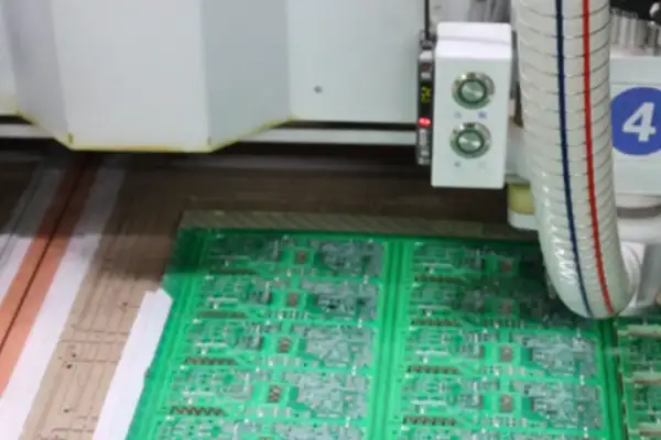
Many people think PCB manufacturing is simply processing according to blueprints, but there’s a lot more to it than that. For example, the copper thickness in high-speed signal traces and the precise positioning of connector pads require extreme care. I once encountered a situation where a slightly off-center pad caused connector contact problems; it took a long time to discover it was a manufacturing error by the board manufacturer. Since then, I’ve paid close attention to whether manufacturers have the capability to perform online testing of these details.
Another characteristic of communication boards is the need to consider long-term reliability. It’s not enough for them to pass the initial test; they must withstand temperature changes and equipment vibration. I value whether manufacturers can provide long-term test data, such as performance trends under high temperature and humidity conditions. While these data points aren’t listed in product specifications, they often reflect the true level of manufacturing processes.
Many manufacturers now boast about their advanced processes, but I believe the key is to solidify the fundamentals. Seemingly ordinary steps, such as thorough post-drilling cleaning and uniform solder mask thickness, are often the most prone to problems. Sometimes, choosing a supplier isn’t about finding the most technologically advanced company, but rather those who take every step seriously.
Another point concerns the design’s ease of maintenance. Communication equipment typically lasts many years, inevitably requiring component replacement. If test points are covered by solder mask or the silkscreen printing is blurry, it creates unnecessary trouble. Good design should simplify later maintenance, not create obstacles.
When choosing communication PCB manufacturing services, many people focus on price, but I’ve found that the real determinants are often the easily overlooked details. I remember once working with a seemingly reputable supplier—they provided complete material certification documents and production process descriptions—but unexpected problems arose during actual production.
On one occasion, we received a batch of boards that passed visual inspection perfectly, but signal transmission instability was only discovered during assembly and testing. An investigation revealed that the supplier had changed the substrate material for the high-frequency materials without informing the customer. Although their test report showed the dielectric constant was within the standard range, differences in the coefficient of thermal expansion between different batches of materials caused micro-stress after lamination of the multilayer boards. This problem wouldn’t surface during routine sampling but would gradually emerge during long-term equipment operation.
This incident made me realize that instead of focusing on whether suppliers could provide perfect written data, it was more important to pay attention to their actual responsiveness. For example, when the material supply chain was strained—would they choose to conceal alternative solutions or proactively communicate and negotiate? We later adjusted our cooperation approach, requiring suppliers to provide third-party test samples with each batch of materials arriving at the factory, and to regularly send representatives to their production quality meetings.
Another easily overlooked aspect is the supplier’s process inheritance mechanism. During a visit to a factory, I noticed an interesting phenomenon: their experienced workers used special calipers to check the edge thickness of the laminated boards—a step completely outside the standard operating procedure. Upon further inquiry, I learned that this was years of accumulated experience—fluctuations in edge thickness could predict changes in inner layer alignment. This experiential preventative measure detected potential problems earlier than instrumental testing.
Now, when evaluating new suppliers, we pay special attention to whether their production line employees possess this proactive intervention mindset. Some companies rely entirely on automated equipment for quality management—which certainly guarantees a basic pass rate—but when encountering new materials or special designs, human experience and judgment are even more crucial.
A recent project further solidified this view—the supplier’s X-ray inspection equipment malfunctioned—normally requiring a production halt for repairs—but their process manager judged, based on copper thickness trends, that production could continue—a decision that proved entirely correct—not only ensuring on-time delivery but also avoiding losses from production line downtime. This kind of intuition built on long-term practice is often more valuable than rigid processes.
Ultimately, good communication PCB manufacturing services are like tacit partners—they not only need standardized production capabilities but, more importantly, the ability to stand by you and solve problems in unexpected situations. After all, even the most perfect contract terms cannot compare to someone willing to double-check the board—to make an extra confirmation call—at a critical moment.
I recently chatted with a friend who works in base station R&D and discovered an interesting phenomenon. The circuit boards their team designed over six months consistently delivered to the factory with subpar performance. Either impedance deviations exceeded standards, or high-frequency signal attenuation was severe. It was later discovered that the problem stemmed from PCB manufacturers’ insufficient understanding of the specific needs of communication products. Many people believe that simply etching the circuitry is enough, but communication PCBs truly test the ability to control electromagnetic wave behavior. For example, in the millimeter-wave band, even micrometer-level linewidth errors can cause phase distortion, requiring manufacturers to master electromagnetic field simulation technology and material property analysis capabilities.
A common misconception is that AI can solve all manufacturing problems. Last year, I visited a PCB factory that claimed to be fully automated. Their AI system could indeed adjust etching parameters in real time. However, the algorithm failed when encountering new substrate materials because the training data lacked attenuation models for the millimeter-wave band. This reminded me of the resonance problem encountered during early testing of five base stations. We had to replace the substrates with three different dielectric constants to find an equilibrium. In reality, AI models need continuous input of the latest test data to remain effective, but the rapid iteration of communication technology often causes algorithms to lag behind by more than six months.
The biggest threat to communication equipment is sudden failures in outdoor environments. I’ve seen a mountain base station experience a complete network outage due to a defect in the PCB’s hole metallization process. Subsequent analysis revealed that the problem was caused by microcracks resulting from fluctuations in the electroplating solution concentration. These kinds of problems are impossible to detect with traditional quality inspection. Now, some manufacturers are embedding sensors into each board to monitor temperature and humidity changes in real time and warn of potential risks. This approach is much smarter than post-construction repairs. For example, embedding miniature humidity sensors at critical nodes on the circuit board can automatically activate heating devices before condensation forms.
When choosing a PCB supplier, don’t just look at certifications. Last year, we compared two manufacturers, both with IATF 16949 certification. Manufacturer A could explain the design logic of each impedance control layer in detail, while Manufacturer B only showed thickness tolerance data. As a result, the boards produced by Manufacturer A had a 40-fold lower bit error rate under extreme temperature testing. True professionalism lies in the depth of understanding of communication principles. For example, Manufacturer A’s engineers proactively suggested using a stepped impedance design to reduce signal reflection; this collaborative design capability is the core competitiveness.
Recently, I’ve noticed a new trend: some small-batch PCB manufacturers are starting to focus on product development for specific frequency bands. For example, a Shenzhen company specializes in 28GHz millimeter-wave board processing. They even built their own anechoic chamber to test field strength distribution. This vertically integrated approach is more adaptable to future needs than a large, all-encompassing production line. After all, the 6G era may require handling terahertz frequency signal transmission. Their developed composite dielectric material can reduce signal loss to 0.2dB/cm, a level that has reached international advanced standards.
Ultimately, technological iteration in the communications industry always outpaces manufacturing standard updates. Ten years ago, who could have imagined that ordinary FR4 material would be unable to meet 5G requirements? Now, we face the heat dissipation challenges posed by gallium nitride power devices. Good manufacturers should have the ability to evolve in sync with R&D, rather than relying on mature processes. After all, no one wants their advanced circuit designs to be ruined by outdated manufacturing processes. For example, leading manufacturers are now testing metal-based composite materials to handle power densities exceeding 15W/mm²; this material innovation is a manifestation of proactive evolution on the manufacturing side.
I have some experience in finding the right communications PCB supplier. I’ve worked with several before; some were indeed professional and reliable, while others fell short. It’s not that they can’t make the boards, but whether they can truly understand your needs and handle the details meticulously.
I remember once communicating with a supplier whose technical team hadn’t even proactively mentioned basic impedance matching; we had to repeatedly press them before they offered a solution. This passive approach is quite inefficient, especially since communication boards have such high signal integrity requirements—even a slight deviation can affect overall system performance.
A good supplier should be involved in the design phase, offering professional advice on aspects like material selection and layer stack-up, rather than waiting until the board is defective and requiring rework.
Many factories claim to manufacture communication PCBs, but their skill levels vary greatly. Some may have complete equipment, but their process control is unstable; a board that passes today might have problems tomorrow with the same parameters. Truly reliable suppliers have a robust MES system that allows for full traceability from material input to shipment.
What I value most is a supplier’s ability to implement robust quality control. For example, details like the storage conditions for high-frequency boards and the temperature profiles for the lamination process often determine the reliability of the final product. Sometimes, visiting their factory to see their production environment and testing equipment is far more effective than looking at brochures.
Another important factor is the standardization of documentation delivery. We’ve previously encountered situations where incomplete test data meant we couldn’t access the original records, making collaborations extremely unsettling. Now, when choosing a supplier, we always confirm their ability to provide complete production data and quality inspection reports.
Finding a communication PCB manufacturing service provider is like finding a business partner; besides technical capabilities, smooth communication and a willingness to invest time in understanding your specific application scenario are crucial. After all, every project has unique requirements, and a one-size-fits-all solution is often unreliable.
The worst scenario is encountering suppliers with exceptionally low quotes but various hidden costs later on. While it may seem like you’re saving money, quality issues could lead to greater losses. I now prefer manufacturers who can clearly explain their cost structure and are willing to invest in the details of the manufacturing process.
While collaborating with a smart wearables team to select a semiconductor flex
We often regard electronic products as a glossy whole, but ignore the
Many assume that choosing China for PCB assembly is solely about saving
- Pienten ja keskisuurten erien tuotannon asiantuntija
- Korkean tarkkuuden piirilevyjen valmistus ja automatisoitu kokoonpano
- Luotettava kumppani OEM/ODM elektroniikkaprojekteihin
Aukioloajat: (ma-la) klo 9:00-18:30.