
Why does your Motor Drive PCB always “retire” early?
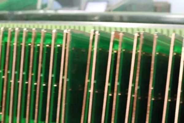
The motor drive circuit board in industrial equipment failed after long-term operation,
China’s circuit board manufacturing sector is currently undergoing a quiet revolution. Many people still cling to outdated impressions of the past—perceiving the industry merely as a hub for simple OEM (Original Equipment Manufacturer) assembly. In reality, today’s PCB factories have long since moved beyond the simple model of merely accepting orders and churning out products.
I recently visited several circuit board factories in the Pearl River Delta region. The workshops were almost entirely devoid of human workers; fully automated production lines handled every step—from drilling to copper plating—in one seamless, continuous process. One factory owner told me that the orders they accept now are almost exclusively highly customized projects. Clients arrive with design schematics and demand that prototypes be produced within just three days—a turnaround speed that would have been utterly unimaginable five years ago.
When discussing the future landscape of China’s PCB industry, I feel that people tend to focus too heavily on raw production capacity figures. What is truly fascinating is the ongoing reshuffling of the entire industry value chain. Smaller factories are facing a stark choice: either shut down or pivot toward specializing in niche board types—such as the flexible circuit boards used in medical equipment. Conversely, larger manufacturers are moving upstream in the supply chain, beginning to conduct their own in-house research and development on core substrate materials.
There is a particularly interesting phenomenon emerging: nowadays, you can even ship circuit board samples from a courier station located in a rural village. What does this signify? It demonstrates that the “capillaries” of the manufacturing sector have successfully penetrated into every single corner of the country. Just the other day, I was approached by an entrepreneurial team based in a small county town; by utilizing PCBs sourced from a local, small-scale factory, they had developed a smart irrigation system with production costs that were half that of comparable products currently on the market.
However, the industry is not without its challenges. I once visited a factory that proudly touted itself as a leader in “intelligent manufacturing,” only to discover that their final quality inspection stage still relied on veteran technicians peering through magnifying glasses. Such manual processes will inevitably be replaced by machine vision systems sooner or later, though the transition itself will undoubtedly require time. I believe that over the next decade, the most exciting prospect is not merely an increase in production volume, but rather the formation of a robust innovation ecosystem. Consider, for instance, how many hardware entrepreneurs today are able to rapidly bring their ideas to fruition—they rely heavily on the agility of the domestic PCB supply chain. It is this capability for rapid iteration—transforming blueprints into physical prototypes with speed and efficiency—that constitutes true competitive strength.
Of course, the challenges are equally apparent. Environmental regulations are becoming increasingly stringent, and raw material prices are subject to significant volatility; yet, these very pressures serve as catalysts, compelling the industry to upgrade. Several manufacturers I know have already begun utilizing recycled materials for their substrates; while this entails higher costs, it aligns with the broader trends of sustainable development.
Ultimately, the upgrading of the manufacturing sector cannot be achieved through mere slogans; it demands tangible progress at every stage of the process. From design software to production techniques, and from quality management to logistics and distribution—the synergistic evolution of this entire value chain is the most accurate reflection of the current state of China’s PCB industry.
During recent conversations with friends involved in foreign trade, I observed an intriguing phenomenon: although the manufacturing sector in Southeast Asia is developing rapidly, orders requiring precision engineering—particularly those for high-precision PCB boards—continue to flow back to domestic manufacturers. This reminds me of a client last year who initially attempted a trial production run of circuit boards in Vietnam; however, due to unstable impedance control, they ultimately transferred the entire order to a factory in Shenzhen. The client had initially chosen Vietnam to capitalize on the local advantage of lower labor costs; yet, during the small-batch trial production phase, they discovered that while basic manufacturing processes met the required standards, the impedance matching required for high-frequency circuits frequently exhibited tolerance fluctuations exceeding the critical technical threshold of ±10%. This was particularly evident in the alignment precision of inner layers within multi-layer boards—Vietnamese factories typically achieved a precision of only 50 microns, whereas Shenzhen-based manufacturers, utilizing direct laser imaging technology, could consistently maintain precision within 20 microns. Such discrepancies directly compromise signal integrity; particularly in applications involving 5G communication equipment and high-frequency radar systems, even minute deviations in impedance can render an entire batch of products unusable.
In reality, while many major international corporations may implement “China-plus-one” contingency strategies, they ultimately remain dependent on our region’s comprehensive supply chain once they reach the mass production stage. During a visit last week to a PCB manufacturing facility in Dongguan, I observed their newly installed vacuum lamination press—a machine capable of completing temperature control calibration within a mere fraction of a second. Such a level of precision is, for the time being, truly irreplaceable. This German-imported lamination press is equipped with an infrared thermal imaging monitoring system, enabling it to scan and map the temperature distribution across every board in real-time throughout the lamination process. When a regional temperature differential exceeding 3°C is detected, the system utilizes 128 independent temperature control units to execute compensations within milliseconds. This dynamic temperature-adjustment capability ensures that the uniformity of the prepreg’s flow characteristics exceeds 98%. In contrast, traditional hot-press machines—still widely used in Southeast Asian factories—rely on manual expertise to adjust parameters; their temperature control precision often hovers around ±15°C, resulting in persistently high rates of substrate delamination and board blistering.
I once discussed with an automotive electronics engineer the current requirements for vehicle-grade circuit boards, specifically their need to withstand temperature cycling tests ranging from -40°C to +150°C. Reliability under such extreme conditions happens to be a particular strength of domestic enterprises; after all, having navigated years of iterative development within the mobile phone supply chain, we have accumulated a wealth of practical experience in High-Density Interconnect (HDI) technology. The domain controller boards designed by their company for new energy vehicles, utilizing Any-Layer HDI technology, feature a 20-layer stack-up with 0.3mm micro-vias. During a cold start at -40°C, this structure must withstand a 0.8% difference in the coefficient of thermal expansion between the copper foil and the base material. Domestic manufacturers—by refining modified epoxy resin formulations and employing specialized brown oxide processes—have managed to maintain bond strength above 12 N/cm; in contrast, comparable overseas products frequently exhibit cracks in the via walls after undergoing 1,000 thermal cycling tests. This technical advantage stems from the mSAP process data accumulated during the early years of smartphone motherboard manufacturing, when the domestic supply chain successfully overcame mass-production bottlenecks for 30μm line-and-space geometries to meet the demand for reducing chip package thickness from 1.0mm to 0.6mm.
However, I have also observed a rather intriguing phenomenon: some small-to-medium-sized PCB manufacturers are now choosing to focus on specific niche segments—such as flexible circuit boards for medical devices or thick-copper boards for industrial control systems. These specialized firms are actually thriving more than those factories that accept every order that comes their way; this strategy of deeply cultivating a specific niche has allowed them to secure an indispensable position within the supply chain. For instance, a factory in Suzhou with a workforce of 200 specializes in ultra-fine flexible PCBs (FPCs) for endoscopes. Their products enable the integration of 12 circuit layers within a flexible tube with an outer diameter of just 1.2mm—a technical barrier to entry that allows them to maintain a gross profit margin exceeding 35%. Another manufacturer specializing in industrial power supplies has developed a unique etching process for 6-ounce thick-copper PCBs. This process enables a via clearance of just 0.5mm while maintaining a board thickness of 3.2mm—a capability that effectively meets the rigorous heat dissipation requirements of megawatt-class frequency converters.
I know a business owner who, three years ago, completely converted his standard double-sided PCB production lines into dedicated lines for Mini-LED backplane boards. At the time, many people considered his move too risky; yet today, their production capacity is fully booked through the second half of next year. This foresight—anticipating and strategically positioning oneself within a niche market segment—is truly admirable. The production lines they invested 20 million RMB to upgrade feature a specialized “roll-to-roll” manufacturing process developed specifically for ultra-thin 0.2mm substrates, effectively resolving the critical issue of board warping during the Mini-LED soldering process. They are now able to supply TV manufacturers with backplane boards boasting a pitch accuracy of 0.15mm—a level of precision 30% higher than the industry standard—which directly secured them an exclusive supply contract with a leading South Korean brand.
Ultimately, the relocation of manufacturing operations is never merely a simple geographical shift; far more critical are the accumulated technical expertise and industrial synergies involved. One might occasionally see news reports about a new factory being built in this or that country, but what truly determines the flow of orders is the comprehensive ecosystem underpinning it all—an ecosystem encompassing everything from material supply and process standards to talent reserves. Take, for instance, the electronic-grade fiberglass cloth upon which the PCB industry relies: the global manufacturers capable of consistently supplying the “1080” model are predominantly concentrated in China’s Jiangsu and Guangdong provinces. Producing this material requires maintaining an extreme level of uniformity, specifically a monofilament diameter of precisely 3.7 microns. While newly established factories in Southeast Asia may boast brand-new equipment, they often still have to import essential chemical reagents from China; moreover, local technical personnel typically require over five years of accumulated experience just to master the precise control of additive concentrations in the copper plating lines. This is to say nothing of the specialized substrates used in the aerospace and defense sectors, where core material formulations and process parameters are regarded by leading domestic enterprises as strategic assets—an intricately interwoven industrial ecosystem that simply cannot be replicated overnight.
Over the years, I have interacted with numerous hardware development teams, and I have noticed that many still harbor an impression of China’s PCB industry that is stuck in the past—specifically, about a decade or more ago. In reality, the landscape today is completely different.
I recall a US-based team approaching us for a potential collaboration last year; their very first question was whether we could drive production costs down to the level typically found in Southeast Asia. It was only after we delved deeper into the conversation that we realized they were completely unaware that leading domestic PCB manufacturers are now capable of achieving line-width precision of just 5 microns—to say nothing of their advanced processing capabilities for specialized materials. This cognitive gap is quite frustrating.
Ultimately, this industry ceased to be driven by low-price competition a long time ago. I know of manufacturers who have invested in as many as seven or eight AOI systems solely for the inspection phase, in addition to developing their own proprietary MES systems to track production data from start to finish. These investments yield more than just improved quality; more importantly, they enable real-time collaboration with clients to address design issues.
A fascinating example of this emerged recently. A medical device company initially approached us merely for contract manufacturing services; however, they soon discovered that our engineers could help them optimize their impedance matching schemes—a contribution that directly boosted their signal integrity by 20%. The value generated by such deep-seated collaboration far outweighs the few percentage points saved by simply driving down the quoted price.
Currently, the most successful enterprises in the industry are pivoting toward offering comprehensive solutions. After all, the barrier to entry for mere circuit board manufacturing is steadily lowering; true competitiveness now lies in the ability to help clients solve their actual, practical problems. Sometimes, the process unfolds like this: a client arrives with nothing more than a preliminary concept, and we collaborate with them every step of the way—from material selection to thermal design—ultimately delivering not just a bare board, but a complete, production-ready solution.
Of course, this transition is not without its challenges. For instance, some long-standing clients remain habitually fixated on price as their primary criterion, requiring repeated dialogue to help them appreciate the true value of technological investment. Yet, this very dynamic underscores the profound transformation the industry is currently undergoing—shifting from a labor-intensive model to a technology-driven one.
Having watched this industry evolve step by step, I believe its most invaluable asset is its pragmatic ethos. Rather than constantly clamoring about “disruption,” practitioners focus on the solid, substantive work of refining processes and optimizing workflows. While the benefits of such incremental accumulation may not be immediately apparent, over time, they coalesce into formidable competitive barriers.
In the final analysis, when selecting a partner today, the critical factor is not the numbers on a price quote, but rather whether the partner can truly grasp your requirements—and even help you identify issues you hadn’t realized existed. This, more than anything else, represents the most compelling value proposition within China’s PCB industry at its current stage of development.
Over the years of engaging with various PCB suppliers, I’ve observed a rather interesting phenomenon: whenever China’s PCB manufacturing capabilities are mentioned, many people instinctively conjure up images of low-cost, mass-produced commodities. In reality, however, the landscape has shifted dramatically.
Just last year, I worked with a factory in Shenzhen that secured an order for the mainboards of a medical device. The project demanded boards featuring embedded components—and, furthermore, required them to successfully pass rigorous biocompatibility testing. Ten years ago, no one would have dared to accept an order like this; yet today, with their full involvement in the design process—from material selection to impedance control—they are able to achieve final yields exceeding 98%. This level of capability cannot be explained away as merely the result of a price war.
When selecting suppliers today, what I value most is their ability to keep pace with our rhythm. For instance, on a project last week, we had to make a last-minute change to the layout of the heat dissipation vents. We sent the requirements over late at night, and their engineers immediately generated alternative solutions on the spot—even taking the initiative to optimize the copper foil thickness while they were at it. Behind this rapid response lies the maturity of the entire supply chain; from substrate supply to etching chemical formulations, every single link in the chain has been meticulously honed by dedicated experts over the course of more than a decade.
Of course, some people worry about the risks associated with over-reliance on a specific geographic region. My approach is to stratify our orders: standard circuit boards are entrusted to specialized “quick-turn” manufacturers in the Yangtze River Delta region, while complex, high-frequency boards are exclusively assigned to two established enterprises with backgrounds in military-grade manufacturing. After all, when it comes to PCBs, a discrepancy of even a single micron can result in a significant drop in performance; there is simply no need to diversify for the sake of diversification alone.
Recently, while conversing with clients in the automotive electronics sector, I noticed that they are paying increasing attention to their suppliers’ carbon footprint records. One factory in Suzhou has even gone so far as to display real-time data from its electroplating wastewater recycling system on a public dashboard; this level of operational transparency has actually become a distinct advantage—a “plus factor”—when it comes to securing international orders.
Ultimately, the Chinese PCB industry has long since moved past the stage of competing solely on price. The competition now centers on who can best accommodate complex technical requirements—and who can introduce innovative design flourishes while simultaneously guaranteeing uncompromising reliability. The next time you are in the process of selecting components or suppliers, I highly recommend seeking the advice of the veteran technicians on the production line; they have likely handled more physical circuit boards than we have ever drafted designs for.
Step into a modern circuit board manufacturing facility, and you will observe a fascinating phenomenon: those very stages of production that were once regarded as technical bottlenecks are now quietly undergoing a transformation. I recently toured several PCB production bases of varying scales—some located in coastal regions, others inland—and they shared a common characteristic: all are actively striving to break free from traditional manufacturing paradigms. These factories no longer view the etching process as a mere chemical treatment step; instead, they have begun to focus on optimizing the overall coordination and synergy of the entire production workflow.
I recall visiting a factory in central China where I observed their etching operations. The engineers explained to me that they had fine-tuned the chemical solution ratios and temperature control protocols. Although this might sound like a minor adjustment, the resulting improvements in performance and yield were remarkably significant. This approach reinforced a realization for me: true innovation does not always require the pursuit of disruptive technological breakthroughs; often, a more practical and effective path lies in the continuous, incremental improvement of existing processes and foundations. Many Chinese PCB manufacturing enterprises are currently making similar attempts. For instance, by introducing real-time monitoring systems to dynamically adjust etching parameters, they have improved the uniformity of copper foil thickness by 15% while simultaneously reducing the volume of chemical waste generated. This process of incremental optimization has not only lowered production costs but also significantly boosted product yield rates.
I have observed an interesting phenomenon: some factories place a particular emphasis on equipment maintenance, while others focus more heavily on operator training. These two approaches, in fact, reflect distinct management philosophies. The former posits that stable equipment serves as the bedrock of quality assurance, whereas the latter maintains that skilled employees are better equipped to handle unforeseen contingencies. From a practical standpoint, however, a combination of both approaches likely represents the optimal solution. For example, one factory implemented a preventive maintenance system to periodically replace wear-and-tear parts, while simultaneously organizing weekly skills competitions to enhance employees’ ability to diagnose equipment anomalies; as a result, their equipment failure rate dropped by 30% year-on-year.
During a conversation with a factory manager, he mentioned that today’s younger generation is generally less inclined to engage in repetitive manual tasks, a trend that has prompted them to accelerate their automation initiatives. However, he also emphasized that automation is not merely about replacing human labor with machines, but rather about fostering a more effective collaborative relationship between equipment and personnel. I find this perspective highly compelling, as even the most advanced machinery still requires human oversight and fine-tuning. His factory addressed this by implementing human-machine interface systems, allowing operators to monitor real-time equipment performance data and empowering them to independently adjust parameters within specific parameters—thereby harnessing the efficiency of automation while preserving the flexibility inherent in human intervention.
During my factory tours, I noticed a specific operational detail: some factories opt to process orders for different clients on separate production lines, while others consolidate orders based on process similarities. The former approach ensures product consistency, whereas the latter enhances equipment utilization efficiency. This seemingly simple production arrangement actually reflects the management team’s differing priorities regarding efficiency versus quality. For instance, PCBs intended for medical equipment are typically processed on dedicated production lines to ensure strict cleanliness standards, whereas PCBs for consumer electronics often utilize a mixed-mode production model to minimize line changeover times.
Many factories today are attempting digital transformation, yet few are truly succeeding. A technical lead once told me that the problem often lies not with the systems themselves, but with the employees’ usage habits. They invest heavily to implement management systems, yet operators remain accustomed to recording data using only pen and paper—a scenario all too common in traditional manufacturing enterprises. To address this issue, some factories have begun adopting a phased training approach: employees first practice on simulated systems, then gradually transition to using actual production data, thereby ensuring that digital tools become truly integrated into their daily workflows.
I believe that the future development of the PCB industry may place greater emphasis on flexibility rather than economies of scale. As product lifecycles accelerate, smaller factories capable of rapidly reconfiguring their production lines may actually hold a competitive advantage. Of course, this requires companies to be thoroughly prepared in terms of both equipment configuration and personnel training. For instance, they might adopt modular production line designs—enabling rapid equipment reconfiguration via standardized interfaces—while simultaneously cultivating a multi-skilled workforce, thereby allowing the factory to complete a product line transition within just 48 hours.
Recently, I’ve observed some factories experimenting with new quality management methodologies—forgoing the traditional “end-of-line” full inspection in favor of shifting the inspection process upstream into the production workflow itself. While this approach increases the initial workload, it effectively reduces subsequent rework costs. From a long-term perspective, this shift is certainly worth noting. In practice, these factories establish rapid inspection checkpoints after every critical process step, utilizing machine vision technology to perform real-time assessments; should any deviation be detected, process parameters are immediately adjusted, thereby nipping quality issues in the bud.
Speaking of circuit board manufacturing, I feel that many people place excessive focus on the so-called “cost advantage.” In reality, labor costs at domestic circuit board factories now account for roughly 10% of total costs—a figure that has more than doubled compared to five years ago. I know several manufacturers in Guangdong who are now more inclined to invest in automated equipment; although the initial capital outlay is substantial, it ultimately results in significant long-term savings on labor costs.
I recently chatted with the owner of a factory in Suzhou, who told me that when accepting orders, he now places a much higher premium on technological sophistication. Standard double-sided PCBs yield razor-thin margins—sometimes netting less than 5% profit—whereas products like High-Density Interconnect (HDI) boards can command profit margins exceeding 15%. This reminded me of a Shenzhen-based company I visited last year; they specialize exclusively in manufacturing circuit boards for automotive electronics—a niche where, despite the high unit prices, customers are practically clamoring to place orders. In reality, the greatest strength of China’s PCB industry isn’t its low cost, but rather the collaborative efficiency of its entire supply chain. From copper-clad laminates to the final finished products, every single stage of production is completed within a radius of just 200 kilometers. The speed advantage generated by this “cluster effect” is what truly makes it irreplaceable. I once needed to rush a batch of prototype boards; I sent the design files on a Thursday afternoon and received the finished products via SF Express by Monday morning. Such turnaround speed is simply unimaginable anywhere else.
While it is true that Southeast Asian nations have recently absorbed a significant number of relocated orders, they primarily focus on the simplest single-sided boards. When it comes to slightly more complex multilayer boards, their yield rates simply cannot hold up. I’ve seen eight-layer boards produced by factories in Vietnam where the circuitry was so crude it looked as if it had been drawn by hand. After all, it takes three to five years to cultivate a skilled process engineer—a challenge that cannot be solved simply by purchasing a few pieces of equipment.
That said, domestic manufacturers are currently facing their own set of difficulties. Environmental regulations are becoming increasingly stringent, and the cost of treating wastewater from electroplating—a critical process—rises every year. These “hidden costs” can collectively account for as much as 20% of a manufacturer’s total operating expenses. One factory in Dongguan, for instance, spent over eight million RMB last year on environmental equipment upgrades alone; such expenditures are ultimately reflected in the final price quotes provided to clients.
I believe the PCB industry will become increasingly segmented in the future. The production of boards for standard consumer electronics may continue to shift toward China’s interior regions or Southeast Asia, but high-end manufacturing will undoubtedly remain concentrated in established hubs like the Pearl River Delta and the Yangtze River Delta. After all, these regions boast not only mature supply chains but also a vast pool of highly experienced veteran craftsmen—assets that cannot be easily replicated elsewhere.
I’ve recently noticed an interesting phenomenon: some foreign clients are actually willing to pay a 10% premium to have their high-end boards manufactured by Chinese firms. When asked why they don’t turn to Korean manufacturers instead, they explain that while Korean technology may indeed lead in certain niche areas, China remains the more reliable choice when it comes to overall manufacturing capability and responsiveness. Perhaps this is the true allure of a fully integrated supply chain.
Ultimately, there are no shortcuts in the manufacturing sector. Simply purchasing a few pieces of advanced machinery does not instantly guarantee the production of high-quality goods; the key lies in the cumulative wisdom and experience gained through years of dedicated practice. As a veteran craftsman I know—someone with twenty years of experience in PCB manufacturing—once put it: “Machines are inanimate; people are the living force.” No matter how sophisticated the equipment may be, it still requires human expertise to calibrate and fine-tune it—a principle that holds true in any manufacturing context. While chatting recently with a few friends in the hardware sector, I noticed that the criteria people use when selecting a PCB supplier today are completely different from those of five years ago. In the past, everyone would obsessively scrutinize—and haggle over—the figures on a price quote; now, however, they place far greater value on supply chain stability and a manufacturer’s accumulated technical expertise. This reminds me of a PCB factory in Dongguan that we worked with last year: although their workshop didn’t have many workers, every production line was equipped with automated inspection systems. Consequently, the boards they delivered were almost entirely free of quality defects.
In reality, China’s PCB manufacturing industry has long since moved past the stage where success depended solely on driving down labor costs. During a visit to Suzhou last month, I observed that factories still relying heavily on manual labor were precisely the ones failing to secure high-end orders. One factory manager told me that while their investment in automation equipment this year did increase upfront costs, the subsequent improvement in yield rates actually lowered their effective cost per square meter by three percentage points. This shift is particularly evident now that even small-batch orders for consumer electronics are beginning to require manufacturers to provide detailed process parameter traceability reports.
On one occasion, we urgently needed to modify a batch of PCBs for medical devices and approached three different suppliers for comparison. The factory in Vietnam offered a genuinely low price, yet the samples they provided suffered from misaligned character printing. The manufacturer in Guangdong was more expensive, but they provided comprehensive material certification reports. Ultimately, we chose the latter—willingly paying the premium—because the product in question was designed to be implanted in the human body. This incident made me realize that simply comparing labor cost figures is no longer meaningful; the true “hidden costs” are embedded within the quality control processes themselves.
There is an interesting phenomenon currently unfolding within the industry: the more a PCB factory emphasizes its low labor costs, the harder it finds it to secure long-term contracts. Just last week, a supplier complained to me that their newly purchased German-made equipment had paid for itself within just two months—simply because their clients were willing to pay a premium for the assurance of stable impedance control. This, perhaps, is the metamorphosis currently taking place within China’s manufacturing sector: we no longer need to justify why our costs are higher than others’, but rather demonstrate why we are worth the price.
Of course, this transition process is bound to come with its share of growing pains. I know of a PCB factory in Zhejiang that, last year, laid off its entire manual drilling team. At the time, the owner was concerned that their production capacity would suffer; however, the newly installed laser drilling machines not only doubled their processing speed but also enabled them to create micro-vias—features that were impossible to achieve using traditional methods. The result of such upgrades is not merely a redefinition of costs, but a fundamental restructuring of the entire industry’s value proposition.
I recently had a chat with a few friends in the hardware sector and noticed an interesting phenomenon. While everyone is discussing the topic of chip self-sufficiency, few realize that PCBs—seemingly such a fundamental component—actually harbor even greater opportunities. We may be overly focused on high-profile concepts like ICs, inadvertently overlooking the fact that foundational elements—such as carrier boards—are what truly determine overall system performance.
I recall a drone project last year where the team spent a fortune customizing specialized chips; yet, due to a flawed PCB design, they encountered severe signal interference issues. Later, they switched to a manufacturer in Shenzhen to redesign the carrier boards, and the problem was resolved. This incident made me realize that the true strength of China’s PCB manufacturing industry lies not merely in its scale, but in its ability to respond rapidly to such specific, concrete requirements. If you visit factories in Dongguan, you can find engineers tweaking design schematics as late as 10 p.m.—this kind of agility is where the real competitive edge lies. This capacity for immediate response is particularly well-suited for customized projects involving small batches and high-frequency iterations—such as the rapid development cycles typical of smart wearables or IoT terminal devices.
Nowadays, when discussing industrial upgrading, many people tend to fixate on the most cutting-edge technologies; however, I believe it is often more important to simply execute existing tasks to absolute perfection. Take server motherboards, for instance: while many manufacturers produce them, some manage to introduce novel innovations in thermal management. Rather than simply “stacking materials” (over-specifying components), they improve heat distribution by refining the routing layout on the carrier boards. Such innovations at the micro-detail level are often far more practical than merely chasing after the latest manufacturing processes. For example, by optimizing copper foil thickness and matching dielectric constants, they can boost thermal dissipation efficiency by over 15% without incurring any additional costs.
I know several business owners in traditional industries who, when attempting to undergo digital transformation, frequently stumble over circuit design challenges. One textile machinery manufacturer, for instance, invested millions in smart upgrades, only to discover that their biggest hurdle was the instability of their control boards. They eventually turned to a manufacturer in Suzhou specializing in industrial-grade PCBs. The solution provided was surprisingly straightforward: targeted optimizations regarding the selection of carrier board materials and protective surface treatments. For instance, by opting for high-Tg (glass transition temperature) TG170 laminates and applying a “three-proof” protective coating, they managed to triple the lifespan of their circuit boards within the harsh, high-temperature, and high-humidity environment of their workshop floor.
Ultimately, a high-quality electronic product is much like a building: a beautiful set of blueprints is not enough; the quality of the actual construction is paramount. In this analogy, the PCB serves as the steel reinforcement hidden within the foundation—it is the critical structural skeleton that ultimately determines how long the entire system will endure and how fast it will run. Nowadays, many startup teams are too eager to achieve quick results; they often skimp on investment in circuit design, only to discover a host of problems once they reach mass production. One smart home team, for instance, suffered a 40% reduction in the communication range of their wireless modules because their impedance control was inadequate.
Interestingly, the more complex a system is, the more critical the importance of the PCB becomes. Consider, for example, the battery management systems in new energy vehicles or the control units in medical devices; in these scenarios, the reliability of the circuit board directly impacts human safety. I have seen manufacturers cut corners on board materials to save costs, only to end up paying aftermarket support costs far exceeding the initial savings. One medical device manufacturer, for instance, was forced to recall an entire batch of products because their use of cheap substrate materials led to a drop in insulation resistance.
In fact, if you observe the hardware companies that have performed well over the past few years, you will find that they have all put immense effort into their PCB designs. Their goal isn’t to pursue the most expensive solution, but rather to identify the implementation method that best suits their specific product. Sometimes, a simple double-sided board—when meticulously designed—can yield better results than blindly stacking multiple layers. The key lies in understanding fundamental principles—such as how current flows and how signals propagate. For instance, rationally planning power supply paths and grounding strategies can effectively mitigate electromagnetic interference.
Recently, I’ve noticed that some young engineers are particularly obsessed with simulation software but are reluctant to spend time performing hands-on soldering and debugging. This reminds me of the veteran craftsmen of earlier eras; simply by touching a board material, they could tell whether it was suitable for high-frequency circuits. While the underlying principles behind such empirical judgments may be difficult to articulate, they often prove more effective in actual production than theoretical calculations. Some veteran craftsmen can even determine whether the reflow soldering temperature met specifications simply by observing the luster of the solder joints—a form of practical expertise that simulation software simply cannot replicate.
Ultimately, building great hardware requires patience and a pragmatic attitude. Rather than spending all day discussing “disruptive innovation,” it is far more productive to ensure that every solder joint is secure and every circuit trace is optimized to its fullest potential. This is the fundamental duty that China’s manufacturing sector should steadfastly uphold.
Over the years, people have often asked me why I insist on keeping our circuit board production within China. The answer is actually quite simple: when you need to simultaneously manage complex manufacturing processes and large-scale mass production, you discover that this region possesses distinct advantages that are truly difficult to replicate elsewhere. Last year, we had a project requiring the production of a 20-layer High-Density Interconnect PCB. We approached several overseas suppliers, but their quotes were either exorbitantly high or they simply stated they couldn’t handle the job. Ultimately, the order was taken up by a long-established factory in Shenzhen. Not only did they deliver on time, but they also helped us optimize several drilling designs, resulting in significant cost savings. For instance, by utilizing laser drilling technology, they were able to reduce the size of vias—originally specified at 0.2 mm—down to 0.1 mm. This approach simultaneously increased routing density and mitigated issues related to interlayer crosstalk. This capability to optimize process details is often rooted in an engineer’s deep understanding of material properties and equipment parameters.
I have interacted with numerous international clients who, at first, approached us with a “let’s just give it a try” mindset, placing only small sample orders in China. However, once they witnessed the actual quality of the finished products and the speed of our response, their attitudes shifted completely. One German client, for example, initially only dared to place a trial production order for 500 units; now, they have shifted the production of even their core product lines over to us. This level of trust was not bought with low prices, but rather built up through a consistent track record of on-time deliveries and rapid responses to issues. I recall one instance where their production line experienced a sudden material anomaly; our engineers worked through the night to adjust plating parameters and air-freighted replacement chemical solutions, ultimately ensuring that the delivery schedule remained on track. This capability for emergency response made the client realize that supply chain stability is far more critical than mere differences in unit price.
Of course, this industry does face its share of challenges—rising labor costs, for instance, are a very real issue. However, what I find truly fascinating is observing the significant investments many factories are making in automation. Last month, I visited a company specializing in automotive electronics; their production lines have already achieved 70% automation, requiring virtually no human intervention from the lamination stage all the way through to final inspection. While this kind of transformation demands substantial upfront investment, it is absolutely critical for enhancing long-term competitiveness. For example, the Automated Optical Inspection (AOI) system they employ utilizes multispectral imaging to detect circuit defects at the micron level—a process that is over five times more efficient than manual visual inspection. This serves as a prime example of how the principles of “Industry 4.0” are being successfully implemented in concrete manufacturing scenarios.
Environmental regulations are becoming increasingly stringent, yet I view this as a positive development; after all, no one wants to pursue industrial growth at the expense of the environment. Many regions are now actively promoting “green manufacturing,” which, for the industry as a whole, presents an opportunity for a strategic realignment. Companies that prioritize environmental compliance and sustainability are finding themselves increasingly favored by high-end clients. Technologies such as cyanide-free gold plating and zero-discharge systems for heavy-metal wastewater—while requiring initial investment to retrofit production lines—ultimately lead to a significant increase in product value and market premium once compliance with standards like the EU’s RoHS directive is achieved. One of our Japanese clients, specifically impressed by our wastewater recycling system, decided to transfer their medical equipment orders from Taiwan to us.
People often cite the low costs in Southeast Asia, but the completeness of a supply chain is something that simply cannot be replicated overnight. To give you an example: if you need to manufacture a substrate using specialized materials, you might be able to source every single raw material supplier right here in Dongguan. If you were to move operations elsewhere, the sheer wait time for materials alone could add an extra two or three weeks to the schedule. The efficiency advantage born of this industrial cluster effect becomes particularly critical when dealing with urgent orders. Last year, during the pandemic, we were able to quickly secure high-frequency copper-clad laminates through our local supply chain; meanwhile, our competitors missed key project milestones due to delays in customs clearance for imports. Such unforeseen events serve to further underscore the immense value of ecosystem-wide collaboration.
I’ve recently noticed an intriguing trend: an increasing number of international brands are establishing their R&D centers in China. This, in turn, is driving technological upgrades among local manufacturers like us. In the past, our role might have been limited to simply manufacturing according to provided blueprints; now, however, clients actively invite us to participate in early-stage design discussions. This model of deep collaboration is fundamentally reshaping traditional OEM relationships. For instance, a U.S.-based firm established its 5G antenna R&D team in Suzhou; working alongside them, we tested over thirty different ceramic substrate solutions, ultimately developing a new product with superior dielectric constant stability. This “knowledge spillover” effect is gradually transforming contract manufacturers into comprehensive solution providers.
Watching this industry evolve—from a purely price-driven battlefield to one that now prioritizes technological accumulation—is truly a poignant experience. Perhaps true indispensability lies not in how low your costs can go, but rather in your ability to continuously generate new value for your clients. Take, for example, the flexible circuit boards we recently developed for a drone manufacturer: by utilizing three-dimensional routing techniques, we managed to reduce the component’s weight by 40%. This level of innovation extends far beyond the traditional scope of contract manufacturing. When you are able to help clients resolve technical pain points they haven’t even recognized yet, the collaborative relationship naturally transcends the simple logic of a buyer-seller transaction.
While chatting with a few friends in the electronics manufacturing sector recently, I noticed an interesting phenomenon: it seems that domestic PCB manufacturers are currently walking a tightrope. On one side, clients are ruthlessly driving down prices—acting as if they expect to buy circuit boards for the price of cabbage. On the other side, environmental protection agencies are tightening their regulations with increasing severity; simply switching on the wastewater treatment equipment now burns through enough cash in a single day to buy a brand-new electric car.
A small factory I know recently installed a new exhaust gas treatment system; the owner remarked that the cost was excruciatingly painful to bear, yet he dared not forgo the installation. After all, a factory in a neighboring town was shut down—literally sealed off—for illegally discharging wastewater; today, weeds are growing right inside its abandoned workshops. Under such intense regulatory pressure, many factory owners have begun contemplating relocating their production lines to Southeast Asia—where, after all, labor costs are lower and environmental compliance thresholds are somewhat less stringent.
But is relocating really that simple? A friend who established a factory in Vietnam recently complained to me that local workers operate at only 70% of the efficiency found back home. Furthermore, the material supply chain is prone to disruptions; if a batch of copper foil arrives just three days late, the entire production line grinds to a halt. When factoring in logistics and management overhead, the ultimate cost savings might actually be less substantial than simply upgrading automation equipment domestically.
Consequently, many factories are now pursuing a strategy of differentiation. They are specializing in high-tech niches—such as high-frequency PCBs or flexible circuits—areas where the technical barriers to entry are so high that ordinary manufacturers cannot even compete. I visited a Shenzhen-based company that has stopped accepting orders for standard double-sided PCBs altogether; instead, they focus exclusively on manufacturing precision circuitry for medical equipment. Although the order volumes are smaller, their profit margins have effectively doubled. Moreover, clients in this sector are less price-sensitive and place a much higher premium on stability and reliability.
Another interesting trend has emerged: whereas factories once viewed environmental compliance as a burdensome expense, some are now leveraging it to secure government subsidies. A company in Jiangsu, for instance, extracts copper from its etching wastewater and resells it to metal processing plants. Over the course of a year, the revenue generated from this recycling process actually covers 30% of their total pollution control costs. This “turning waste into wealth” approach is far more astute than merely going through the motions to pass regulatory inspections.
Ultimately, the PCB industry has long since moved past the era where profits were driven by sheer manpower. Success today hinges on finding the optimal balance between cost efficiency and regulatory compliance. Those factories that still rely on cheap labor to undercut competitors and secure orders will likely not survive the industry consolidation and shakeout expected in the coming year. (Specific Case Detail: That Shenzhen-based company recently secured an order for the mainboard of a surgical robot. The circuitry required a tolerance of just 0.05 millimeters, necessitating specialized adjustments to their electroplating parameters and the real-time monitoring of temperature and humidity levels throughout the workshop.
The motor drive circuit board in industrial equipment failed after long-term operation,
Many 5G antenna PCB designs rely too much on simulation, but ignore
While collaborating with a smart wearables team to select a semiconductor flex
- Pienten ja keskisuurten erien tuotannon asiantuntija
- Korkean tarkkuuden piirilevyjen valmistus ja automatisoitu kokoonpano
- Luotettava kumppani OEM/ODM elektroniikkaprojekteihin
Aukioloajat: (ma-la) klo 9:00-18:30.