

Why the Best PCB Supply Chains Are Built Like Relationships, Not Transactions: Lessons for Satellite Communication PCB Programs
What actually makes a long-term PCB supply chain partnership work — shared
Many people assume that installing a protection board on a battery makes the system safe. That assumption is wrong enough to cause serious problems. A device that runs normally and then cuts power unexpectedly — and the investigation revealing a cold solder joint on the SMT PCBA — is not an unusual failure pattern. It is a reminder that engineering attention has been concentrated on “function” and almost nothing on the physical reality of how the board lives inside a product.
The Battery Protection PCB Assembly is not an isolated module. It is installed inside a battery pack where it must withstand vibration, face temperature cycling, and handle parameter drift as cells age. Engineers routinely design the schematic, validate that over-charge and over-discharge protection triggers correctly in bench testing, and consider the work complete. This misses the question that actually matters: how does this assembly survive inside the product over its service life?
What the Schematic Cannot Specify
A concrete example: placing the sense resistor at significant distance from the main control chip and routing a fine trace between them. From the schematic perspective this is completely acceptable. On the actual SMT PCBA, that long thin trace is vulnerable to interference from surrounding high-current lines. The resulting sampling offset — perhaps a few millivolts — may seem trivial. But for a lithium cell working near its 4.2V full-charge state, a few millivolts of error can mean protection triggers earlier or later than designed. Neither outcome is desirable.
The testing environment compounds this problem. Standard laboratory testing is static testing: simulate an over-current condition, verify that the protection board responds. But the real test is what happens after the product ships. Summer heat in a vehicle, winter cold, sustained vibration from power tools or balance scooters — these are the actual conditions the PCB must survive. Under these conditions, will solder joints crack from thermal expansion and contraction? Will SMT components detach from sustained mechanical shock? These failure modes are invisible to functional testing, which is precisely why responsible production processes add mechanical stress and environmental stress validation — vibration table runs, dozens of thermal cycling passes through a temperature chamber, followed by functional verification of protection behavior.
These steps add cost and time. They are worth it. A battery with high enough energy density to require serious protection cannot be guarded by a fragile board. The board’s robustness must receive the same engineering attention as its functional specification.
The Protection IC Needs a Clean Signal Environment
The protection IC is a precision instrument. It continuously monitors cell terminal voltage and current flow, then makes decisions based on preset rules. But the thresholds it enforces are not universal. A board configured for standard lithium-ion at 4.2V full charge, applied to lithium iron phosphate cells that saturate at approximately 3.65V, is a category mismatch. The starting point for every design is the specific cell chemistry’s datasheet. Those pages define the only valid basis for all protection thresholds. “Standard values” do not exist. Manufacturer-specific variations in over-discharge protection voltage, for example, may differ by 0.3V while carrying significant implications for cycle life.
The IC’s own power supply quality directly affects its measurement accuracy. If the supply line runs adjacent to motor drive circuitry or switching regulator nodes, the resulting noise causes the IC to make incorrect judgments. Correctly powered cells may trigger false over-charge alarms. Protection that should activate may respond sluggishly.
In SMT PCBA layout, the filter capacitor belongs immediately adjacent to the IC’s supply pin — “immediately” is critical, because lead inductance undermines high-frequency filtering. A 100nF ceramic capacitor handles high-frequency noise, while a parallel electrolytic capacitor stabilizes lower-frequency supply variations. The IC’s ground connection must reference a quiet zero-potential point — never shared with the high-current power ground.
Voltage sampling lines must come directly from each cell’s positive and negative terminals as dedicated conductors. Allowing them to share any portion of a high-current copper path introduces the resistive voltage drop in that copper section as a systematic measurement error. Ten amperes through a five-milliohm path produces fifty millivolts of drop — enough to push voltage monitoring outside its safe window, causing protection to act too early or too late.
Physical Isolation: The Principle Behind Reliable Layout
The most dangerous assumption in protection PCB design is that protecting high-voltage components on one side of a schematic line completes the isolation. The physical layout is the actual test.
A well-executed layout separates the main protection circuit from any secondary protection circuit with independent ground plane sections allocated to each, preventing common-mode failure paths. The main current path — connecting the cell terminals through the MOSFETs to the load — should be designed as short and direct as possible, with all current returns going through a controlled path that keeps high-frequency switching return currents away from the sampling ground reference.
One project encountered persistent instability that simplified architecture eventually resolved. The original design used multiple IC layers collaborating on a shared voltage reference network. When that reference source showed drift, every protection channel was affected simultaneously. Simplifying to a minimal hardware protection loop with fewer shared nodes produced more consistent behavior. The principle the experience illustrated: more components means more potential failure points, and every component shared between protection channels is a potential common-mode failure path.
When relay drive transients create coupling into adjacent sampling circuits, the correct fix is designing the relay drive as a system-level problem — identifying the coupling path during layout planning and providing dedicated inductive return paths — not adding filters after the symptom appears. Building this discipline into the layout from the start produces boards that do not need remediation.
MOSFET Selection, Placement, and the Operating Temperature Reality
Most engineers evaluate MOSFETs at 25°C. This is an unreliable basis for protection applications. Battery protection boards routinely reach operating temperatures well above 100°C during high-load operation. At elevated temperatures, on-resistance increases by 30 to 50 percent relative to room-temperature values. If design calculations use room-temperature parameters, actual thermal dissipation is systematically underestimated.
MOSFET thermal management begins at placement. Surrounding a MOSFET with other components and placing it at the board’s thermal center creates a heat trap. Positioning devices at board edges, adjacent to copper pour regions with thermal via connections to adjacent layers, gives heat a conduction path outward.
Thermal via arrays beneath power component pads are critical for this conduction path, but their quality matters as much as their quantity. Under-plated vias — thin copper walls that do not substantially fill the via barrel — conduct heat no better than the surrounding substrate and fail the thermal design purpose. The design must specify plating quality requirements for thermal vias, not just geometric patterns.
One comparison result that reframes the MOSFET selection discussion: two otherwise identical designs with MOSFET positioning at board edges versus board center showed peak device temperature differences exceeding 15°C under identical load. That 15°C difference matters substantially for device lifetime under continuous operation.
The body diode reverse recovery characteristic deserves specific attention in protection applications. During the charging cutoff transient, current may briefly flow through the body diode. If that diode’s turn-off is slow — carrying significant reverse recovery charge — the resulting voltage spike can stress or damage the protection IC. In fast-charge applications with high current slew rates, a MOSFET with poor reverse recovery can produce overshoot exceeding the absolute maximum rating of adjacent components, creating failure modes that are intermittent and difficult to reproduce.
Parallel MOSFET Configurations Require Physical Symmetry
Parallel MOSFET configurations require physical symmetry, not just electrical equivalence. Devices from the same production lot share similar initial characteristics, but routing path length differences, impedance asymmetry, or asymmetric thermal coupling cause unequal dynamic current sharing. The device that runs hotter draws more current through the thermal runaway dynamic, until it fails first. Symmetric routing — equal path lengths, similar geometries, matched gate drive conditions — is what prevents this, not identical part numbers.
Gate resistor selection for protection MOSFET drive requires testing-based calibration, not simple adoption of datasheet recommended values. Different applications require different switching speeds. Too fast produces voltage overshoot from stray inductance; too slow affects efficiency and increases thermal load. The balance point requires iterative characterization.
A technique that addresses voltage overshoot risk proactively is pre-reserving layout space for snubber circuits and protective devices at critical locations. These may not be populated in initial production, but their positions being available allows rapid response if testing reveals overshoot that must be managed.
SMT Process Quality as the Foundation of Long-Term Reliability
Reflow temperature profile control is more consequential than it appears in production decisions. A peak temperature five degrees above optimal, or a ramp rate slightly too fast, creates internal stress in solder joint metallurgy that is invisible at electrical test. Six months after deployment, in a product experiencing daily thermal cycling between operating and storage temperatures, those stressed joints begin to fail.
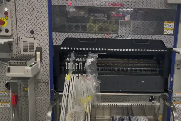
For MOSFET packages with large thermal pads, the reflow challenge is particularly demanding. If the board’s ground plane beneath the thermal pad conducts heat away aggressively during reflow, the solder paste at the thermal pad may not reach adequate liquidus temperature. The visual appearance of the connection can look acceptable while the actual metallurgical bond is inadequate. X-ray inspection of completed assemblies reveals what optical inspection cannot: solder void percentage, joint height uniformity, and absence of bridging beneath area-array packages.
Solder paste management is a frequently underestimated variable. Paste that has not been properly temperature-conditioned before use, or that has been open to the manufacturing environment beyond its working time, changes its rheological properties. The resulting solder joints may look acceptable under visual inspection but have different microstructure and fatigue characteristics than joints produced from properly managed paste.
Dynamic testing is substantially more predictive than static testing. Measuring standby current, verifying protection voltage thresholds with DC equipment, and confirming MOSFET on-resistance in static conditions constitute the minimum baseline — not sufficient validation. Protection circuits must respond correctly during dynamic events: instantaneous short circuits, motor startup current peaks, charger plug-insertion voltage transients. Adding dynamic short-circuit tests and high-intensity pulse load tests to production validation requires additional equipment and process time. The alternative — discovering these failure modes in the field — costs far more.
Threshold Setting: Conservatism as Engineering, Not Timidity
A protection threshold is not a number from a datasheet. It is a number chosen with knowledge of the specific application context, expected component variations, and the realistic noise floor of the measurement environment. Setting thresholds at their theoretical limits to maximize claimed usable capacity produces a system that triggers protection at unexpected times under real conditions. Over-discharge protection set at the absolute minimum may cause unintended shutdowns at low temperature, where cell internal resistance rises and terminal voltage sags faster under load.
The engineering philosophy that produces more reliable protection boards uses deliberately conservative thresholds — accepting a small capacity reduction in exchange for noise immunity and robustness to component aging. A threshold that appears slightly suboptimal in a clean bench measurement will behave correctly across the range of manufacturing tolerance, environmental variation, and cell aging that characterizes real deployment.
Pursuing extreme response speed by sacrificing noise immunity produces a board that cuts power when a nearby motor starts, generating poor user experience. Increasing filter time to suppress noise means real short-circuit events encounter protection response that arrives after the damage has occurred. The robust solution is deliberate calibration based on the specific application’s noise environment and acceptable response characteristics — not theoretical extremes in either direction.
Material Compatibility Over the Product Lifecycle
Material compatibility across the assembly’s life cycle is an underexamined category. Conformal coating materials, adhesives used for component fixation, and potting compounds all exist in chemical contact with PCB substrates, component encapsulation resins, and potentially electrolyte vapor. Slow chemical degradation over years can raise conductor resistance, reduce insulation resistance, or introduce intermittent conductivity. One specific failure traced to this mechanism: a silicone adhesive used to secure a power component produced gradual impedance change in that region over months, creating an anomalous resistance in the current path that was effectively invisible until the protection function began responding inconsistently.
Pre-production compatibility verification through extended exposure testing prevents this. Discovering the failure mode six months after a production release does not.
PCB board material selection deserves more attention than it typically receives in protection applications. Standard FR4 under sustained high-voltage exposure can gradually age, with insulating properties declining over time. For high-reliability applications — high-voltage, high-energy-density battery packs — materials with higher CTI values resist electrical tracking failures more effectively and extend board life in humid environments. The cost premium for these materials is recoverable within the first avoided field failure event for products in demanding service conditions.
Spot-Welding Interface Design: The Thermal Paradox
The spot-welding attachment point between the protection board and battery cells presents a specific thermal design paradox. Standard thermal design for PCB power components emphasizes maximizing heat dissipation. For the spot-welding pad, this logic inverts.
The spot-welding process uses a brief, intense electrical current pulse to generate localized resistive heating at the contact point, fusing the nickel strip to the copper. If the welding pad connects to a large copper pour or inner-layer ground plane, that copper mass absorbs the welding energy faster than the pad region can heat to fusion temperature. The weld appears visually complete but has not achieved adequate metallurgical bonding. Applied tension separates it easily.
The design response is deliberate thermal isolation at the spot-welding pad — only a narrow trace or a restricted copper path connecting the pad to the circuit. This allows welding energy to concentrate at the contact point and reach fusion temperature. The principle is opposite to standard SMT thermal design, and applying standard thermal thinking to the spot-welding pad produces systematic bonding failures.
The protection board that performs reliably through the product’s service life is the product of discipline applied consistently at every stage: material selection, layout architecture, MOSFET placement and drive, SMT process controls, dynamic validation, and long-term compatibility verification. No single stage is sufficient, and no stage can compensate for failures at another. The engineering investment required to get every stage right is the investment that determines whether the protection claim is real — or whether it is a specification that exists only in the test fixture.
What actually makes a long-term PCB supply chain partnership work — shared
Practical, experience-based strategies for how to reduce PCB procurement risks — from
Real factory-floor lessons on how to optimize a PCB manufacturing process —
- Pienten ja keskisuurten erien tuotannon asiantuntija
- Korkean tarkkuuden piirilevyjen valmistus ja automatisoitu kokoonpano
- Luotettava kumppani OEM/ODM elektroniikkaprojekteihin
Aukioloajat: (ma-la) klo 9:00-18:30.
Get quote, solution or any question, Andre always here to help