
Heat Dissipation Challenges and Solutions in PCB Circuit Board Design
Circuit boards are more than just that green board in a phone
I’ve always felt that many people’s focus on thick copper PCBs is somewhat misplaced. Everyone loves to stare at those complex testing processes, as if simply listing a long enough number of test items guarantees quality.
In fact, from our actual production perspective, the key to whether a 4 oz copper PCB is usable often lies in the most basic steps.
Take copper foil as an example. Many people think that as long as the thickness meets the standard, it’s fine. However, what truly affects soldering quality is the surface treatment process. I’ve seen too many cases where top-quality materials were used, but improper storage conditions led to copper foil oxidation, resulting in the entire batch of boards having to be reworked.
There’s a particularly interesting phenomenon: some manufacturers, in pursuit of so-called perfect data, set extremely rigid testing standards. For example, they require all line widths to be accurate to three decimal places, neglecting the more important issue of current-carrying uniformity.
I remember last year helping a client analyze a batch of faulty boards. They had previously focused all their efforts on visual inspection, using the most expensive scanning equipment to check for micron-level defects. But they ultimately discovered the problem lay in the simplest continuity test—improper pressure settings on the test probe caused some connections that should have shown errors to be forcibly connected.
This reminds me of an analogy: it’s like buying a house and focusing on the wallpaper pattern, forgetting to check the structural integrity of the load-bearing walls.
Currently, there’s a worrying trend in the industry: over-reliance on automated testing equipment. Machines can indeed detect defects invisible to the human eye, but determining whether these defects affect usability still requires experience.
For example, a slight scratch on the copper foil surface might be completely negligible on a power board, but in a high-frequency circuit, it could cause signal reflection problems.
We recently adjusted our quality control process, focusing on functional testing rather than aesthetic perfection. After all, circuit boards are meant to be used, not displayed in a museum.
Sometimes customers ask why our tolerances are more lenient than others. My answer is simple: we focus more on the board’s performance under real-world operating conditions. Rather than pursuing perfect data in the lab, it’s better to simulate multiple real-world usage scenarios.
Ultimately, good quality control should be like a skilled traditional Chinese medicine practitioner taking a pulse—it requires understanding instrument data and, more importantly, making comprehensive judgments.
By the way, the heat dissipation of thick copper plates is also a common misconception. Many people think that the thicker the copper, the better the heat dissipation; however, the thermal conductivity of the substrate must also be considered.
Last week, I encountered a case where a client insisted on using ultra-thick copper foil for their LED driver board. This resulted in uneven heat conduction and localized overheating. Switching to a moderate thickness with a better heat dissipation design significantly improved performance.
Therefore, my advice is not to be intimidated by various testing requirements. Understanding the fundamental principles is more important. After all, even the most advanced equipment is just a tool; the true determinant of quality is the depth of understanding people have of the product’s essence.
What do you think?
Seeing more and more electronic products moving towards high power, I’ve been wondering: can traditional circuit boards really withstand the load? Last year, while working on an industrial power supply project, I encountered a particularly interesting phenomenon—when the same design drawings were submitted to different manufacturers for prototyping and testing, the performance differences were over 30%. Upon disassembly and comparison, the problem was found to lie in the most basic PCB material.
One supplier insisted on using standard 1-ounce copper foil, resulting in voltage fluctuations after less than two hours of full-load operation, while another supplier using 4-ounce copper foil remained stable even after eight hours of continuous stress testing. This stark contrast made me realize that in high-power scenarios, board thickness is not an option, but a crucial factor determining success or failure. Especially when handling instantaneous high currents, those microsecond-level pulses, invisible to the naked eye, create a striking skin effect on thin copper foil.
I remember once visiting an automotive electronic control unit production line and seeing them deliberately set the ambient temperature to 85 degrees Celsius during aging tests on motor drive boards. An engineer pointed to a running 4 oz copper PCB and said that under such conditions, ordinary circuit boards would have already delaminated and blistered, but their products were guaranteed to be fault-free for ten years. Later, when we developed our own photovoltaic inverters, we adopted this approach, specifically designing a 4 oz thick copper area under the heatsink to disperse the accumulation of heat spots.
Many of my peers are still fixated on circuit precision, but I believe we should focus more on the physical characteristics of the current path. Just like a river irrigating fields, a shallow channel will overflow during a downpour, while a sufficiently deep channel can balance the flow. Recently, while testing a new servo driver, I found that changing the power layer to 4 oz thick copper directly reduced the temperature rise by 15 degrees Celsius—an improvement far more effective than changing any thermal paste.
There’s actually a simple way to determine if a PCB needs thickening: touch the hottest area of the board when it’s in operation. If you have to pull your hand back within three seconds, then you should consider upgrading the copper foil. Last time I helped a friend modify a drone’s ESC, the originally paper-thin power supply lines were replaced with a 4oz design, and the flight time unexpectedly increased by 7 minutes. This is probably a hidden benefit of low impedance.
Sometimes, looking at those failed samples emitting blue smoke in the lab makes it clearer that the essence of high-power design isn’t about piling on components, but about maintaining just the right amount of margin in every aspect. Just like building a house with a deep foundation isn’t for showing off, but to ensure the entire building stands firmly in the face of storms.
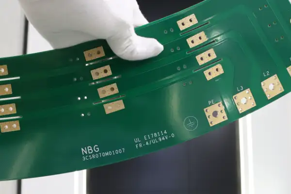
I’ve seen many people struggle when choosing a 4oz copper PCB manufacturer. Actually, it’s not that complicated.
Some people immediately focus on all those fancy certifications. I’m not saying certifications aren’t important—they do reflect a manufacturer’s basic compliance level—but the key factors that truly determine whether a PCB is usable are often more practical.
I remember once we needed to make a batch of PCBs for industrial control boards. One supplier proudly displayed their ISO certificates. However, the first batch of samples showed noticeable burrs on the circuit edges – a problem that would definitely cause issues at high temperatures.
Later, switching to a smaller manufacturer solved the problem. While they didn’t have as many certificates, they showed us their process records for handling 4oz copper foil and photos of similar projects they’d done before – that’s what you call reliable! So now I value a manufacturer’s actual experience handling similar complex projects more than just what’s on paper.
You have to understand that 4oz thick copper foil is prone to over-etching during etching – this directly affects the final circuit’s precision and current-carrying capacity – something not just any manufacturer can control! Some manufacturers might be fine with regular thin copper boards, but their shortcomings become apparent when faced with such special requirements!
I’ve also noticed something interesting: many people overly rely on imported equipment while neglecting the importance of experienced operators – even the most advanced machines need knowledgeable people to calibrate them, otherwise they’re just a pile of scrap metal! Once, I visited a factory where their drilling machines were indeed the latest models, but the young man in charge of programming clearly lacked understanding of the characteristics of thick copper, resulting in very poor hole wall quality!
Therefore, when I evaluate suppliers now, I pay special attention to the actual experience of their technical team—especially the special cases they’ve handled and their problem-solving approaches! This is much more reliable than simply looking at what equipment they have or how many certifications they possess!
Ultimately, the most crucial thing when choosing a 4oz copper PCB manufacturer is whether they have real skills, not just superficial claims! After all, your product ultimately speaks for itself based on its actual performance!
Every time I see articles discussing PCB design emphasizing how important heat dissipation is, I want to laugh. They always portray high-power applications as technical challenges that require special materials to solve.
I worked on an industrial controller project using a standard 4oz copper PCB design and didn’t encounter the legendary heat dissipation bottleneck problem at all. The key was to make the power circuit layout reasonable, avoiding crowding heat-generating components together. Sometimes, adding a few more grounding vias is much more practical than worrying about copper thickness.
Many people, upon hearing “high current,” immediately think of using thicker copper foil, pursuing specifications like 4oz, but neglecting the most basic wiring logic. A customer once insisted on cramming a motor drive module into a tiny space, resulting in overheating even with a thicker PCB. Later, adjusting the component spacing and using ordinary board material solved the problem.
In the automotive electronics field, there’s a constant emphasis on high temperature and vibration resistance, as if survival depends on special processes. However, in reality, many controllers operate in environments far from their limits; over-design only adds unnecessary costs. I’ve seen many battery management boards for new energy vehicles that could operate stably for ten years using conventional processes, yet some insist on piling on components.
What truly needs attention is long-term operational stability, not extreme test data from the lab. I’ve handled a batch of servo drives that ran continuously in the factory for over three years using only a basic 4oz copper PCB, never failing due to temperature rise. Conversely, those devices pursuing complex heat dissipation solutions often introduce new failure points due to complex processes.
Ultimately, PCB design needs to fit like clothing; thicker isn’t always safer. You have to choose based on the actual current and space constraints. Sometimes, blindly adding more copper is like wearing three layers of cotton clothing in winter—inconvenient and wasteful of materials.
I’ve always felt that the most easily underestimated aspect of PCB design is the chain reaction caused by material selection. Last year, while working on a motor drive project, I tried using a standard 1-ounce copper-thick board to debug a high-current circuit, and the heat generation was a real headache. Only after switching to a 4-ounce copper foil version did I realize the significant difference.
Many people think that thicker copper is just for carrying more current, but its impact on the overall system temperature distribution is more crucial. In one test, I specifically touched the surface temperatures of the two boards under the same load. The power devices on the standard board were noticeably hot to the touch, while the 4-ounce copper foil version dissipated heat more evenly, with even the edges only feeling warm.
This difference is actually due to the laws of physics. Copper itself is a good conductor of heat. When localized heat is generated, a thicker copper layer can quickly direct the heat energy to a larger area, like providing multiple evacuation channels for the heat source instead of blocking it in a small area. From a thermodynamic perspective, the increased heat capacity resulting from thicker copper foil is equivalent to having a built-in distributed heat storage device, which can smooth out temperature spikes caused by instantaneous power fluctuations. Especially in pulsed operating modes, a thicker copper substrate can absorb heat generated by short-term overloads, preventing overheat protection from being triggered.
I also noticed a detail: on ordinary PCBs, additional heat sinks or potting are often required, but with a thicker copper substrate, these auxiliary methods can be simplified. Sometimes, the copper surface on the back of the board can even be used directly as a heat sink, saving the weight of a metal casing. This shift in design thinking made me realize that thicker copper not only improves heat dissipation performance but can also restructure the entire thermal management system architecture. For example, in space-constrained embedded devices, by rationally arranging thicker copper areas, a heat conduction path similar to a heat pipe effect can be formed, guiding heat from the core heat-generating area to the device casing or interface areas.
However, thick copper design is not a panacea. I’ve encountered people who blindly pursue extreme thickness, resulting in damage to fine signal lines during etching due to insufficient linewidth precision. Therefore, the key is to balance current requirements and process limitations. Sometimes, a mixed layer stack is more practical than a uniform thickness across the entire board. In practical applications, I often employ a partitioned design strategy—using 4 ounces of copper in the power circuit region and maintaining a standard 1-ounce thickness in the digital signal region. This hybrid structure ensures current carrying capacity while avoiding impedance runaway problems caused by differences in etching factors. Especially in high-frequency circuit design, the impact of copper foil roughness on signal integrity must be considered; the more pronounced unevenness of the thicker copper surface may increase skin effect losses.
What truly solidified my choice of this type of board material was an unexpected discovery: when the lab’s air conditioning malfunctioned and the room temperature soared to 35 degrees Celsius, ordinary samples successively shut down under protection, while the board using 4 ounces of copper foil maintained full-power operation. The peace of mind provided by this stability was more convincing than any parameter. This experience led me to delve into the material’s thermal reliability coefficient, discovering that the current carrying capacity decay curve of thicker copper boards at high temperatures is much smoother. When the ambient temperature rises from 25°C to 85°C, the allowable current density of ordinary copper foil decreases by nearly 40%, while 4 ounces of thick copper only decreases by about 15%. This characteristic is particularly important for industrial equipment that needs to cope with sudden environmental changes.
Seeing power supply designs struggling in high-temperature environments now always reminds me of my own experiences plagued by heat dissipation problems. Sometimes, the solution isn’t simply to add more components; changing the basic material can open up new possibilities. Of course, whether or not to use thicker copper depends on the specific application scenario, as cost and manufacturing complexity are real issues, but it’s certainly an option worth considering. Especially in fields with extremely high power density requirements, such as electric control systems for new energy vehicles and servo drives, thicker copper design is becoming a key technological path to improve system reliability. Once, while participating in a photovoltaic inverter project, by increasing the copper thickness of the DC bus section from 2 ounces to 6 ounces, we not only reduced the peak operating temperature by 22°C but also unexpectedly found that the failure rate of switching devices decreased by nearly 30%. This fully demonstrates that the implicit benefits of high-quality substrates often exceed expectations.
I’ve recently been pondering something: why are more and more circuit board designs favoring thicker copper layers, especially specifications like 4 oz copper PCBs?
I used to think that as long as a circuit board could conduct electricity, the thickness didn’t matter. But I’ve discovered that’s not the case at all. Once, during a project I was involved in, we struggled with heat dissipation issues, eventually resolving the problem by using a 4 oz copper PCB. Since then, I’ve paid close attention to this detail.
I think many people underestimate the importance of etching technology in thick copper PCB fabrication. Etching thin copper PCBs is relatively simple, but with increased thickness, poor control can easily lead to side etching or uneven circuitry, directly impacting circuit stability and lifespan.
I’ve seen manufacturers cut corners in the etching process to save time, resulting in boards that quickly malfunctioned under high loads—a lesson I learned the hard way.
Modern electronic devices are increasingly powerful, demanding higher heat dissipation. Thin copper layers simply can’t withstand the heat buildup; over time, performance suffers, and components may even burn out.
I remember a friend who made a power module initially using a standard PCB, which failed aging tests. He only passed by switching to a 4 oz copper PCB. This experience reinforced my belief that copper thickness is not a negligible parameter in certain applications.
Of course, not all circuits require such a thick copper layer; it depends on the specific needs. Blindly pursuing high specifications will only increase costs, so there’s no need to simply follow the trend.
I think that with future technological advancements, the manufacturing process for thick copper PCBs will become more mature, and costs are expected to decrease, leading to wider applications. However, that’s all in the future; for now, we still need to choose based on actual needs.
Furthermore, I’ve noticed significant differences in the quality of thick copper PCB manufacturing among different manufacturers. Some can’t even guarantee basic uniformity, which tests their technological accumulation and process control. Don’t just order based on the cheapest price.
In short, my experience is that if a project has high power or heat dissipation requirements, investing more thought in the copper thickness selection for the PCB is worthwhile. Otherwise, rework after problems arise is a real hassle.
I always laugh when I see people agonizing over whether to use 4-ounce copper foil in their PCB designs. It’s not that complicated.
I’ve seen too many engineers choose ordinary 1-ounce boards to save costs and end up making mistakes. Last year, a friend who works on charging stations stubbornly used thin copper boards, and the circuitry started smoking during full-load testing. If they had used 4-ounce boards, this problem wouldn’t have occurred.
Do you know what’s most ironic? Many people think that thicker copper foil is only for handling high currents, but heat dissipation is the hidden benefit. I once tested an inverter with the same power; a board using 4 ounces of copper foil had a temperature that was more than ten degrees Celsius lower than a board with ordinary copper foil, effectively doubling the lifespan of components. This effect is more practical than adding any heatsink.
However, to be honest, not all projects require piling on components. I usually first look at the peak current; if it consistently exceeds 20 amps, then I generally need to consider 4 ounces. Otherwise, the voltage drop in the circuit will give you a headache, not to mention the temperature rise issue.
Now, some manufacturers recommend ultra-thick copper boards without warning, which I think is a pure waste of resources. Unless you’re making welding machines or industrial-grade frequency inverters that handle hundreds of amps, 4 ounces is sufficient for most scenarios.
The real test of skill is how to maximize the advantages of thick copper, such as through reasonable layout to distribute heat evenly rather than piling it up for excessive heat. Many beginners easily overlook this.
Ultimately, choosing a PCB is like choosing shoes—the most important thing is that they fit. Don’t just look at the parameters; you need to consider the actual application scenario.
I’ve always felt that PCB designers rely too heavily on automated routing software, sometimes neglecting the importance of basic materials. Recently, I used a 4 oz copper PCB for power module testing and discovered a difference – with the same layout, the temperature rise was more than ten degrees Celsius lower than with ordinary boards. This is mainly because thicker copper foil has lower thermal resistance and higher thermal capacity, allowing it to quickly conduct heat from critical components to the entire board surface, and then dissipate it through ventilation holes or external heat sinks. For example, in switching power supplies, if the heat generated by MOSFETs and inductors cannot be dissipated in time, it can lead to shortened component lifespan or even failure.
I remember encountering a strange phenomenon last year when debugging base station equipment: despite sufficient theoretical calculation margin, voltage fluctuations always occurred in hot weather. It was later discovered that this was caused by impedance changes in ordinary PCBs under high loads. Replacing it with a thicker copper board solved the problem. Ordinary 1 oz copper foil, at an ambient temperature of 85°C, may experience an impedance increase of about 15% when a 30A current is applied, while the impedance change of 4 oz copper foil is less than 5%. This stability is particularly important for precision analog circuits and RF circuits; for example, the power supply ripple of a 5G base station power amplifier module directly affects signal quality. Many AI hardware marketing campaigns emphasize the advanced computing chips but rarely address the bottlenecks of the power system. This is like equipping a sports car with a poor-quality fuel line – even the most powerful engine won’t perform. I’ve seen servers where insufficient PCB current carrying capacity caused voltage drops, actually slowing down the entire system. Specifically, when a GPU cluster is simultaneously accelerating computation, the instantaneous current can exceed 200A. If the copper thickness of the power distribution network (PDN) is insufficient, it can cause a voltage drop, triggering the chip’s protection mechanism and causing it to throttle. Some data centers have to deploy additional voltage compensation circuits, which actually increases system complexity and cost.
During a factory visit, I saw them using thick copper plates for inverter heat dissipation tests. Ordinary boards overheated and triggered protection mechanisms within half an hour, while the thick copper plates continued to operate. This direct comparison was more convincing than the datasheet. The tests, using thermal imaging, showed that ordinary boards had obvious hot spots under the power devices, with temperature gradients as high as 50°C, while the thick copper plates had more uniform heat distribution, with the maximum temperature difference not exceeding 15°C. This thermal management advantage is particularly crucial for the electronic control systems of new energy vehicles, effectively preventing IGBT breakdown caused by localized overheating. The use of thick copper PCBs in the military industry is not without reason. It’s not just about current carrying capacity, but more importantly, long-term stability. Ordinary circuit boards may begin to age after a few years, but thick copper structures can withstand more frequent thermal expansion and contraction. In aerospace equipment, circuit boards must withstand cyclic temperature differences from -55°C to 125°C. The ductility of thick copper can alleviate stress caused by CTE mismatch in the substrate, preventing solder joint cracks. Accelerated aging tests on a satellite power module showed that boards using 3 oz copper foil retained over 95% of their initial performance after 1000 temperature cycles.
Currently, some designers cut corners in the power supply section to reduce costs, which actually increases later maintenance costs. Especially for equipment like outdoor base stations that need to operate year-round, the loss from a single failure can be far greater than the cost of the saved materials. For example, the power boards of a certain operator’s mountain base stations, using ordinary thick copper, had a failure rate as high as 12% within three years. Each repair required a professional team, costing over ten thousand yuan per repair. However, if a thick copper board design had been adopted from the beginning, the overall life-cycle cost would have been reduced by more than 30%.
I believe the industry should prioritize the selection of fundamental materials rather than blindly pursuing new processes. Just like building a house with a weak foundation, no matter how beautiful the decorations are, it’s useless. In fact, the combination of new materials such as high thermal conductivity substrates, metal substrates, and thick copper technology is giving rise to a new generation of power electronics design. For example, some high-end server power supplies have begun to use copper inlay technology, embedding copper pillars directly under the chip, reducing thermal resistance to 1/5 of traditional designs. This innovation based on material physics properties is more effective in solving reliability issues at high power densities than simply reducing linewidth.
Every time I see someone treating a 4-ounce copper-thick PCB as a regular board, I want to remind them that these are completely different things. I remember last year a customer came to me complaining about his power supply board design, saying that the same design worked fine on a regular board, but after switching to a thick copper board, it suffered various short circuits and burnouts. Upon opening the file, I found that he had simply applied the design parameters from a 2-ounce board to a 4-ounce board without even adjusting the plating time.
The via-filling process for thick copper boards requires a great deal of experience. While standard resin formulations can fill the pores of ordinary boards, 4-ounce boards often have larger pore diameters, making them prone to invisible shrinkage marks during resin curing. In one experiment, we used three resins of different viscosities and discovered that adding a specific filler allowed the resin to maintain stability at high temperatures. This detail determines whether delamination will occur during subsequent lamination.
Regarding electroplating, I strongly disagree with practices that prioritize speed. Some people forcibly increase current density to shorten lead times, resulting in dendritic crystal formation on the hole walls. In reality, pulse plating, although time-consuming, ensures the copper thickness at the bottom of deep holes meets standards. We tested samples with continuous electroplating where the thickness in the middle of the hole was 40% thinner than at the ends, while the pulse process controlled the difference to within 10%.
Many people easily overlook the heat capacity changes caused by copper thickness in the surface treatment process. For the same specifications, hot air leveling requires extended preheating time for thick copper boards; otherwise, the tin-lead alloy on the surface will develop an orange peel texture due to excessive temperature differences. One factory insisted on using the temperature profile of ordinary boards for our 4-ounce samples, resulting in micro-cracks in the gold finger area, ultimately requiring a complete rework.
In terms of quality control, I trust physical testing more than pure data monitoring. For example, ultrasonic scanning can detect hidden delamination issues earlier than electrical testing. Once, a batch of boards passed all parameters, but X-ray inspection revealed a 0.1mm air bubble in the plug of a grounding via. This detail caused creepage during high-voltage testing.
Now, for thick copper projects, I advise clients to allow sufficient time for process verification. In a previous automotive electronics project, we spent two weeks specifically adjusting plating parameters to achieve a uniform plating layer on vias with an 8:1 aspect ratio. This investment, while seemingly increasing costs, actually avoided the risk of scrap during mass production.
The biggest mistake in thick copper board manufacturing is blindly applying experience. Every step requires a complete rethinking of the underlying logic. It’s like changing the cooking temperature; all the ingredient ratios need to be adjusted. Those who try to use standard processes to handle special requirements often pay a higher price.
I’ve always felt that choosing PCB materials is like choosing clothes for circuit design—the thickness must be determined by the context. I remember last year when designing an outdoor solar controller, the client insisted on using a 4oz copper PCB, resulting in copper foil delamination around the heat dissipation holes. It was later discovered that the problem stemmed from a mismatch in the thermal expansion coefficients of the copper foil and the substrate. At high temperatures, the thick copper actually became a burden.
Many people blindly pursue thick copper PCBs, as if thickness directly equates to reliability. In reality, increasing copper foil thickness exponentially increases etching difficulty. I once saw a factory achieve such severe side etching with 4oz traces that the line width deviation exceeded 30%. What truly needs attention is the uniformity of current density distribution—localized overheating is often more fatal than overall insufficient current carrying capacity.
I once tested and compared performance in different scenarios: in applications like motor drive boards where instantaneous current surges occur, 4oz could indeed withstand the impact; however, in high-frequency signal boards, the skin effect of thick copper actually increased losses. This made me realize that there is no one-size-fits-all formula for PCB design.
A recent automotive electronics project I’ve worked on is even more interesting—they’ve started using different thicknesses of copper foil on the same board. The power supply section uses 4oz to handle high currents, while the signal area uses thin copper to ensure precision. This approach is much smarter than simply piling on thickness, since copper foil is not just a conductive material but also a participant in the thermal management and mechanical structure of the entire system.
Ultimately, thickness is just a number on a parameter sheet. The real test of skill lies in ensuring the thickness of the copper foil serves the actual needs of the circuit. Just as a tailor wouldn’t use wool for summer clothes, good design always starts with function and works backward to choose the material.
The most ingenious example I’ve seen is a solution that shapes the thick copper area into heat sink fins—solving the conductivity problem while also replacing part of the heatsink’s function—this kind of thinking is the wisdom engineers should strive for, isn’t it?
Remember when I first encountered high-power circuit design? Back then, I was struggling with whether or not to add a heatsink to solve the heat problem. Later, an experienced engineer told me: “Instead of going through the trouble of adding a heatsink, just thicken the traces.” This made me start paying attention to different PCB board sizes, especially that seemingly robust 4 oz copper PCB.
Many people’s understanding of circuit boards is still stuck at the stage of ordinary double-sided boards, thinking that as long as the traces are connected, it’s fine. But when you’ve actually handled high-current projects, you’ll understand that a standard 1 oz copper-clad board struggles under high loads like drinking water through a straw. I worked on a solar controller project where using standard board material resulted in a significant voltage drop at high temperatures.
That experience made me realize the importance of choosing the right board material. Now, seeing those power supply designs still using thin copper boards makes me feel like they’re taking a detour. After all, current carrying capacity isn’t something you can imagine; it’s determined by the material’s properties.
I later specifically tested boards of different thicknesses and found that 4 oz copper PCBs had a particularly significant advantage in heat dissipation. In one comparative test, after running for half an hour, the temperature rise of the thick copper board was almost 15 degrees Celsius lower than that of the ordinary board. This difference could translate to a difference in stability and failure rate in practical applications.
However, to be honest, thick copper boards aren’t a panacea. They are indeed more difficult to process, especially the fabrication of intricate circuits, which requires more specialized etching techniques. But if you’re making high-power equipment, this investment is absolutely worthwhile.
Recently, while helping a friend upgrade an old device, I encountered a similar situation. The original design used ordinary board material, which frequently overheated and triggered the protection mechanism. After switching to 4 oz board material, the problem was solved. This tangible result further convinced me that in certain specific fields, material selection is often more important than the circuit design itself.
Seeing more and more industrial equipment adopting this specification is a good sign. It shows that people are starting to value the basic materials rather than blindly pursuing complex circuit designs. Sometimes, the most direct solutions are hidden in the choice of the most basic materials.
I’ve always felt that those who shy away from 4-ounce copper-thick PCBs are being overly cautious. Yes, the etching process is indeed a hurdle—when facing that thick layer of metal, the “side etching” problem is more noticeable than with standard thinner boards. But this doesn’t mean there’s nothing that can be done.
In fact, I encountered a similar situation in my first project: we were using standard thickness boards with extremely fine wiring; however, during production, we discovered that “side etching” had caused some connections to almost break—this made me realize that sometimes “thickness” is actually an advantage! Because when your PCB substrate is solid enough, the increased stability from improved current carrying capacity can completely offset those minor “precision losses.”
Furthermore, I’ve noticed that many people are overly reliant on “high-precision equipment”—as if it’s impossible to do anything without imported machines… But what’s the reality? With proper adjustments to the “chemical concentration” and spray angle, even manual operation can achieve quite good results—of course, this requires some experience—but it’s better than just waiting, right?
I remember last year a customer insisted on extreme “linewidth,” resulting in a board that looked like a spider web… Later, they changed their approach, using wider traces with “4-ounce copper foil,” and the overall performance improved significantly. So, don’t be intimidated by so-called “technical bottlenecks”; often, it’s just a matter of not having the right mindset.
I’ve seen many people overcomplicate multilayer boards. The real headache isn’t the number of layers, but the details hidden within.
I remember once discovering an interesting phenomenon while working on a 4-ounce copper PCB—drilling holes on a regular board might seem instantaneous, but on this type of board, the hole walls look completely different.
Many people think that choosing the right material is all that’s needed, but from the moment you decide to use thick copper, the entire processing chain changes accordingly.
Once, during testing of boards from different suppliers, we discovered significant differences in the actual performance of copper foil of the same nominal thickness after lamination. Some areas appeared smooth, but micro-cracks appeared at the edges after drilling.
This made me realize a problem: we’re too used to applying standard procedures to all situations, but when faced with specific needs, that so-called experience can become an obstacle.
For example, in the drilling process, many people’s first reaction is to switch to a more expensive drill bit, but I found that the real key is controlling the feed rate. Too fast, and it can damage the copper foil; too slow, and it generates excessive heat, affecting the hole wall quality.
One case left a deep impression on me: a client requested a batch of high-reliability boards. We followed the standard procedures, and the initial inspection was satisfactory, but after aging tests, we found a small number of holes showing delamination.
Later, disassembly and analysis revealed the problem lay in the pre-plating treatment—although the surface looked clean, microscopic residues affected the adhesion.
This experience taught me that sometimes we focus too much on macroscopic parameters and ignore the interactions at the microscopic level.
Now, whenever I encounter a thick copper plate project, I pay special attention to two points: first, the stability between material batches; and second, the smoothness of the connection between each process.
After all, a good result is never the perfection of a single link, but the synergy of the entire chain.
Circuit boards are more than just that green board in a phone
From disassembling old routers to visiting electronics manufacturing plants, I gradually realized
As an electronics enthusiast, I’ve come to understand firsthand the impact of
- Pienten ja keskisuurten erien tuotannon asiantuntija
- Korkean tarkkuuden piirilevyjen valmistus ja automatisoitu kokoonpano
- Luotettava kumppani OEM/ODM elektroniikkaprojekteihin
Aukioloajat: (ma-la) klo 9:00-18:30.