
How to Improve PCB Manufacturing Quality Control Process?
In the PCB manufacturing process, we once experienced a large number of
Why is it becoming increasingly difficult to make PCBs smaller?
Recently, while chatting with fellow hardware designers, the conversation turned to PCB prototyping. They all lamented how challenging it is to reduce circuit board size these days. This reminded me of the pitfalls I encountered early in my career; back then, I naively thought that simply connecting all the traces was enough—only to be completely overwhelmed when I first attempted to design a four-layer board.
In reality, many novice designers instinctively rely on traditional through-hole vias. After all, they are the most intuitive option: a single via running straight from the top layer to the bottom layer looks clean and straightforward. However, the downside is obvious—they take up a vast amount of precious routing space. Imagine a pillar running from the roof down to the basement; every room on every floor has to make space for it, and valuable routing channels are ruthlessly wasted in the process.
Why do complex multi-layer designs rely on specialized vias?
It wasn’t until I started working on more complex multi-layer board projects that I realized things were far from simple. I remember designing peripheral circuitry for a processor; even with an eight-layer stack-up, I couldn’t complete the routing and was at my wit’s end. Finally, a seasoned veteran at the manufacturing plant offered a suggestion: “Why not try routing these critical signal groups using blind vias?” Skeptical but willing to try, I modified the design—and to my surprise, the routing was successfully completed.
That experience gave me a profound understanding of the specific use cases for different types of vias. Traditional through-hole vias offer reliable connections and a mature manufacturing process, making them ideal for applications where space constraints are not critical or where robust mechanical connections are required—such as for power pins or mounting screws. However, their drawbacks become glaringly apparent when dealing with dense data buses or high-frequency signals; the massive through-hole structure disrupts signal reference planes and introduces unwanted parasitic parameters.
How do unassuming buried vias become a secret weapon for boosting performance and reliability?
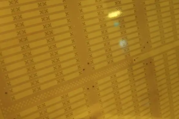
What truly impresses me are the internally buried vias—interconnect channels hidden within the circuit board that do not connect to any outer layers. Their greatest advantage lies in their ability to seamlessly connect sensitive traces—such as those linking to power planes—without consuming valuable surface real estate for component placement, all while effectively mitigating the risk of electromagnetic interference. I once designed an RF module that required a large clearance area on the top layer for an antenna, necessitating that all traces and vias be concealed within the inner layers; this is where the immense utility of buried vias became fully evident.
Of course, discussing these advanced manufacturing techniques inevitably raises the issue of cost. Standard through-hole vias benefit from the most mature processing technology and the lowest prices, making them easy for almost any manufacturer to produce. In contrast, complex stack-up designs incorporating blind and buried vias exponentially increase manufacturing difficulty. Designers must carefully consider alignment precision across dielectric layers, the compatibility of thermal expansion coefficients among materials, and the thermal stresses generated during the lamination process.
I have seen novice designers blindly pack designs with blind and buried vias in pursuit of a “high-end” aesthetic, only to see production yields plummet and costs skyrocket. In reality, many applications can be successfully addressed using simple traditional through-hole vias combined with sensible layout planning; there is no need to adopt new technologies simply for the sake of using them.
How can you make a wise choice regarding via types based on actual project requirements?
Ultimately, selecting the right type of via is like choosing the right tool—the key is to clearly define your actual needs. If you are designing a simple control board or power module, traditional through-hole vias are perfectly adequate; why invite unnecessary trouble and complexity? However, if you are designing motherboards for next-generation smartphones or backplanes for high-speed servers, mastering advanced interconnect technologies—including blind vias—is an indispensable core skill.
There is no “one-size-fits-all” answer here; practical intuition is gained only through repeated cycles of design and prototyping. Engaging in multiple rounds of prototyping and communicating deeply with the factory’s process engineers is far more direct and effective than simply reading through volumes of theoretical material.
Additionally, there is a detail regarding factory communication that warrants special attention: different manufacturers may use slightly different terminology for the same processes. Before placing an order, it is best to clearly communicate specific design requirements and technical specifications to avoid misunderstandings that could delay the project.
Why is systematic process coordination more important than relying on a single piece of advanced equipment?
I often feel that current discussions on circuit board manufacturing go off track; many people become obsessed with impressive-sounding terminology and technical minutiae while overlooking fundamental systems-engineering principles. Take blind vias, for example: people often rave about the precision and sophistication of laser drilling, acting as if adopting cutting-edge equipment will instantly solve every problem.
This is a common misconception. In many projects I have encountered, bottlenecks in the PCB phase rarely stem from obscure technical complexities; instead, they arise from errors in basic material selection or a misunderstanding of the process flow. For instance, consider whether the type, thickness, and surface roughness of your chosen copper foil are compatible with the subsequent laser drilling parameters. You might invest in high-end laser equipment capable of drilling perfect holes, yet end up with rough hole walls and poor copper deposition results—rendering the board unable to meet electrical performance requirements—simply because the copper foil used in an earlier step was unsuitable. It is akin to mounting top-tier racing tires on a car with poorly tuned suspension; even the best tires cannot compensate for the underlying chassis issues.
The true key lies in the systematic coordination and synergy of the entire manufacturing process. This process is akin to a symphony where precision machining and chemical engineering harmonize; yet, while many remember the “symphony” aspect, they often overlook the requirement for perfect synchronization among all performers. Your design blueprints establish the musical score’s framework, while the chosen materials determine the quality of the instruments themselves. A high-quality substrate paired with the right type of copper foil creates a stable platform for subsequent laser processing. When the laser beam strikes the material, it does more than simply ablate a micro-via; the interaction triggers complex physical and chemical changes.
How should we view the interconnection points hidden within multilayer boards and the challenges regarding their reliability?
Many people consider the invisible details of PCB design to be inconsequential—a view I held myself when I first entered the industry, only to realize later that the reality is quite different. Take “blind vias” as an example: the quality of these internal connections cannot be assessed from the outside. Essentially, they are formed by drilling between inner layers to create an interconnection without penetrating the outermost layers—hence the name. While the concept may sound mysterious, the core challenges boil down to two points: precisely forming the micro-via and ensuring the long-term reliability of its mechanical strength and electrical connectivity.
Today, laser ablation is the mainstream method for forming micro-vias. While it offers high precision, it is extremely demanding regarding substrate material properties. Even with perfectly calibrated processing parameters, the resulting inner walls can still be rough or uneven, preventing the plating solution from flowing in properly and rendering the entire process a failure.
The electroplating stage is where a manufacturer’s technical prowess is truly tested. Because these vias are enclosed, controlling the internal chemical reactions uniformly is difficult. Traditional DC plating methods often leave voids at the bottom or result in an overly thin copper layer, which is prone to cracking under thermal shock. Many advanced facilities now employ pulse plating technology, allowing copper ions to build up layer by layer from the bottom to fill the micro-via completely. However, the chemical formulations and process controls involved are as precise as a chemistry experiment; even the slightest deviation can lead to vastly different results. This demonstrates that behind a seemingly simple internal interconnect lies a complex, rigorous manufacturing system; from initial material selection and the setting of processing parameters to final chemical treatments, a failure at any single stage can compromise the entire project. I have encountered numerous cases where the design itself was flawless, yet the manufactured boards failed after a period of use. Troubleshooting often revealed the root cause at these internal interconnects—hidden defects planted during production that standard factory testing had failed to detect.
This experience taught me that in this industry, one should not place blind faith in trendy processes or high-end equipment. It is far more important to thoroughly understand the underlying physics and chemistry of each manufacturing step and identify the approach best suited to your product’s positioning and reliability requirements. After all, not every circuit demands peak performance, but long-term operational stability is a threshold every deployed printed circuit board must meet. Ultimately, hardware development requires a healthy respect for the invisible details of a design; you never know when or where one of them might teach you a profound lesson.
How can we ensure a pragmatic and reliable design while pursuing high-density interconnects?
Over my years in PCB design, I have noticed that many people are intimidated by high-density interconnect technology, viewing it as an unfathomably complex field; in reality, it is not as complicated as imagined. Take blind vias, for example: their fundamental purpose is to save layout space by routing traces from a crowded surface layer to an inner layer, thereby freeing up valuable real estate for surface-mounted components. Consider the many consumer electronics on the market today—such as increasingly feature-rich smartwatches—where the usable internal space is no larger than a fingernail; without such technologies, accommodating all the necessary circuit functions would be impossible. I have encountered engineers early in their careers who are eager to jump straight to the most advanced design solutions, believing that using cutting-edge technology automatically elevates the product’s tier. This is, in fact, a significant misconception. High-end HDI (High-Density Interconnect) PCBs involve more layers and complex blind via stacking configurations, exponentially increasing the stringency of raw material and process control requirements. In many scenarios, a simple four-layer board with “1st-order blind vias” fully meets performance needs while offering higher manufacturing yields and better cost control. Blindly pursuing higher-end specifications not only drives up manufacturing costs but can also introduce hard-to-manage process risks—such as misalignment or incomplete via filling—that ultimately compromise product reliability.
True engineering prowess lies not in the flashiness of the design itself, but in the ability to refine product performance for maximum stability and reliability within cost constraints and existing manufacturing capabilities. Consider automotive controllers: they must operate reliably for over a decade amidst constant vibration, shock, and extreme thermal cycling—requirements far more rigorous than those for the motherboard of an ultra-thin smartwatch. In this context, the critical factors for success are fundamental manufacturing details: can your interconnect structure (including blind vias) withstand long-term thermo-mechanical stress? Is the internal electroplated copper uniform and dense? Simply comparing who uses “higher-end” technology holds little practical significance.
Therefore, my view is that one should not be intimidated by a barrage of technical jargon; terms like “HDI” are essentially tools for solving problems. The value of a tool lies in its effectiveness in achieving goals, not in using it to signal technical sophistication. An excellent design is the result of an elegant balance between functional requirements, long-term reliability, manufacturability at scale, and total cost. Instead of obsessing over whether a specific high-end technology is mandatory, it is better to calmly analyze the actual needs: what signal transmission speed does the circuit require? How constrained is the layout space? What level of manufacturing precision can the project budget support? Once these questions are thoroughly considered, the appropriate technical path becomes clear. Ultimately, this industry is constantly evolving; a process considered high-end today may well become the standard tomorrow. While maintaining a mindset of continuous learning is important, it is even more crucial to develop a comprehensive judgment based on engineering practice and real-world conditions—knowing how to select the technical solution that best fits a specific application scenario. This pragmatic capability is far more valuable than merely chasing what is new, cutting-edge, or novel in technology.
In the PCB manufacturing process, we once experienced a large number of
Conventional materials often fall short when circuit boards must handle high-power or
Looking for a reliable automotive PCB manufacturer? The real criteria go far
- Pienten ja keskisuurten erien tuotannon asiantuntija
- Korkean tarkkuuden piirilevyjen valmistus ja automatisoitu kokoonpano
- Luotettava kumppani OEM/ODM elektroniikkaprojekteihin
Aukioloajat: (ma-la) klo 9:00-18:30.