
Battery Monitoring System PCB: Why the Hardware Foundation Determines Everything Else
BMS reliability isn’t decided by algorithms — it’s decided by the PCB
I’ve been pondering something lately: we constantly talk about how electronic products are becoming smaller and more powerful, yet very few people truly take the time to understand the technology quietly underpinning it all. Whenever a new smartphone or smartwatch is unveiled, everyone marvels at the screen’s clarity and the device’s powerful features; meanwhile, I’m always left wondering: just how much hardware is actually crammed inside such a tiny object to make it function?
It turns out the reality is quite fascinating. A friend of mine, a hardware design engineer, told me that many high-end devices today simply cannot function without a circuit board technology known as HDI. I used to think a circuit board was just a flat green panel covered in wiring; however, after hearing his explanation, I realized that couldn’t be further from the truth.
The scope of HDI PCB applications is far broader than I had ever imagined. It extends beyond consumer electronics—such as smartphones and computers—to include smart systems in automobiles, precision instruments in medical equipment, and even various industrial devices. One example he cited left a particularly strong impression on me: many modern smartwatches can monitor heart rate and blood oxygen levels, as well as handle phone calls and text messages. Packing so many functional modules into such a tiny watch casing would be utterly impossible without high-density circuit board design.
I subsequently did some research of my own and discovered that the core concept behind this technology is actually quite clever. Unlike traditional circuit boards, which are limited to routing connections on a single flat plane, HDI technology operates more like a set of building blocks, utilizing three-dimensional space to its full advantage. By creating multiple layers of interconnections within the board itself, it allows for a significantly greater number of components to be packed into a limited physical space. This reminds me of the Tetris games I played as a child, where skilled players could always fit blocks of various shapes together seamlessly, leaving no gaps.
Once, I took apart an old fitness tracker, and I was truly astonished when I saw the circuit board inside. That board was barely larger than a fingernail, yet it was densely packed with intricate circuitry—some lines were so fine they were almost invisible. At that moment, I wondered just how precise the manufacturing processes must be to create something like that. I later learned that this is the transformative impact of HDI (High-Density Interconnect) technology; it grants circuit designers greater freedom, ensuring they are no longer constrained by spatial limitations.
Nowadays, many electronic products are trending toward being lighter, thinner, and more multifunctional—a trend that is likely to continue. I believe that in the future, we may witness the emergence of even more unexpected product form factors—perhaps mobile phone screens that can be rolled up, or health-monitoring devices as thin as a sticker. The realization of these innovations is inextricably linked to advancements in underlying technologies, particularly improvements in circuit board design capabilities.
Sometimes I wonder: why do average consumers rarely pay attention to these foundational technologies? Perhaps it is because they remain hidden deep within the products—out of sight and out of touch. Yet, every smart device we use on a daily basis ultimately benefits from these technological strides.
From my perspective, the evolution of HDI technology is not merely a matter for the manufacturing sector; it actually reflects the broader societal evolution of our demands for electronic products. We crave more portable devices, greater functionality, and longer battery life; ultimately, all these consumer demands trickle down to the most fundamental technological layers, driving fields like PCB design to innovate continuously.
I recall that the first smartphone I bought years ago was significantly thicker and heavier than today’s models. At the time, it felt incredibly advanced; yet, looking back now, those products clearly had ample room for design optimization. The fact that modern smartphones can deliver such powerful performance within such slim bodies is largely attributable to the optimization of internal component layouts—a feat that would be impossible without the support of High-Density Interconnect technology.
In the future, as IoT devices become ubiquitous and wearable electronics continue to evolve, the demand for miniaturized, high-performance circuitry will only intensify. I believe this field holds a wealth of untapped possibilities waiting to be explored. Perhaps one day we will see completely transparent, flexible circuit boards, or electronic circuits capable of self-repair—who knows? Technological innovation invariably brings surprises.
Whenever I see those incredibly thin, foldable smartphones, I find myself wondering: are we becoming too obsessed with simply making things smaller? Everyone talks about how HDI PCB applications drive device miniaturization—and while that is certainly true, I feel this perspective is somewhat narrow. The real revolution, perhaps, lies not merely in shrinking the motherboard down a little further.
What I have observed is the design freedom unlocked by HDI technology. The devices that have excited me most over the past few years are not the conventional, rigid-slab flagships; rather, they are the diverse array of foldable-screen products. HDI technology is the unsung hero behind their emergence—and their evolution into reliable, practical devices. This high-density interconnect technology allows engineers to pack complex circuitry into extremely limited spaces while simultaneously ensuring signal integrity.
This isn’t just a matter of size. Having disassembled several foldable devices from different brands, I noticed an intriguing phenomenon: to withstand the physical stresses imposed by repeated folding, engineers have had to fundamentally rethink the entire motherboard layout. They no longer chase maximum stacking density; instead, they prioritize balancing stress distribution with thermal dissipation pathways.
I recall a conversation with a hardware engineer who shared a detail that left a lasting impression on me. He explained that when developing an inward-folding smartphone, the greatest challenge wasn’t simply making the motherboard thinner, but rather ensuring that critical components on the board avoided the bending zone while maintaining stable high-speed signal transmission. Ultimately, they adopted a “hybrid-order” HDI design, applying varying routing densities to different regions of the board.
This shift in mindset is where the true fascination lies. Nowadays, when launching new products, many manufacturers love to emphasize the specific HDI “order” used or the percentage increase in routing density; however, I believe these figures hold little significance for the average user. For instance, a motherboard might employ “any-layer interconnect” technology to achieve line widths of less than 10 microns—but the more pertinent question is how that translates into a user-perceptible benefit, such as smoother screen folding or reduced network latency during gaming. Engineers have begun to act like architects planning load-bearing walls, partitioning the PCB into dynamic and static zones—positioning core components like the processor and memory in “safe zones” far removed from the hinge, while meticulously arranging flexible circuits and sensors within the movable regions.
What users actually perceive is whether a device operates smoothly and durably, offers robust battery life, and maintains stable signal reception; it is in enabling these tangible experiences that the true value of HDI technology resides. For instance, more precise routing reduces signal crosstalk, enabling 5G and Wi-Fi antennas to operate efficiently even within compact spaces; meanwhile, an optimized power delivery network design directly boosts energy efficiency, allowing the battery to last longer within a slim, lightweight chassis. None of this can be achieved merely by shrinking dimensions; it demands a systematic design philosophy centered on reliability.
I even believe that in the coming years, we will witness the emergence of electronic products with truly unconventional form factors—perhaps not smartphones, but other types of portable devices. The designs of these devices will be bolder and more eclectic, because engineers know they have technologies like HDI backing them up; this allows them to experiment with greater creativity in circuit design without being shackled by traditional spatial constraints. Imagine a rollable tablet, or a fully functional smartphone that wraps around your wrist like a bracelet—the feasibility of such conceptual products is skyrocketing as HDI technology matures. It liberates not only physical space but, more importantly, the imaginations of product managers and designers.
So, stop fixating solely on the technical specifications listed in data sheets. Instead, look at how these technologies transform the realm of product possibilities—how they make the tools in our hands better tailored to our needs. That is the most fascinating aspect of technological progress. Innovation truly begins when we stop asking, “How thin is it?” and start asking, “What unprecedented things can it do?”
As for those still debating which manufacturing process is “more advanced” based on raw data, I view that as little more than industry-internal navel-gazing. For those actually engaged in creating products, flexibly utilizing existing tools to solve specific problems is far more important—and far more practical—than chasing after a single, isolated technical metric. It is akin to a carpenter who doesn’t merely boast about the sharpness of his chisel, but focuses instead on how to use it to carve out exquisite patterns. In the realm of consumer electronics, what ultimately wins over users is a reliable, surprising experience that seamlessly integrates into their lives—not a bolded, magnified technical buzzword flashed during a product launch presentation.
While chatting with some friends in hardware design recently, I noticed an interesting phenomenon: whenever the topic of HDI PCB applications comes up, many people immediately think of smartphones or computer motherboards. That is certainly not incorrect. However, I feel this perspective is actually somewhat limited. What I find truly fascinating about HDI technology is the way it is quietly transforming fields that we often tend to overlook.
Take, for instance, a small medical device R&D firm I visited not long ago. At the time, they were designing a portable health monitor. This device—barely larger than a standard power bank—needed to integrate ECG monitoring, blood oxygen detection, and basic body temperature recording capabilities. The engineers told me that the standard multi-layer PCBs they initially used simply couldn’t accommodate so many chips and sensors; they only managed to resolve the issue after switching to HDI boards utilizing micro-via technology.
This reminded me that, all too often, when we discuss technological progress, we tend to fixate on the flashiest, most cutting-edge products—such as the latest smartphones or concept cars. Yet, in reality, high-density interconnect technologies play an equally critical role within industrial equipment that may appear ordinary, or even somewhat mundane.
I have a friend who works in an automated manufacturing plant; he is responsible for maintaining the vision inspection systems on the production line. He explained that the volume of image data captured by their high-speed cameras is immense; even the slightest interference or latency in the transmission lines can cause the entire inspection process to fail. However, after upgrading their control boards to incorporate more sophisticated HDI designs, they saw a significant improvement in both signal integrity and noise immunity—which, in turn, boosted their overall production efficiency.
Of course, many people today tend to associate the advancement of AI with hardware development—and while that is certainly a prevailing trend, I believe it would be an oversimplification to view AI as the sole driving force behind the demand for HDI technology. In fact, the digital transformation currently underway in many traditional sectors—such as monitoring equipment for energy grids or data acquisition stations for agricultural environments—is also placing increasingly high demands on device reliability, miniaturization, and data processing capabilities. These requirements are similarly compelling PCB technology to evolve toward higher densities and more complex designs.
Therefore, I believe we should broaden our perspective when considering the applications of HDI PCBs. They serve not only the consumer electronics market or the frontiers of high-tech innovation; in many fundamental yet vital sectors, they are quietly underpinning the stable operation of entire systems. It is this broad and profound impact that, perhaps, constitutes their true value.
During recent conversations with friends who work in circuit design, I noticed an interesting phenomenon: whenever the subject of high-density interconnect technology comes up, many people immediately think of smartphones or computer motherboards. This is actually a rather narrow view. In reality, over the past few years, HDI technology has been quietly transforming the landscape of various industries in places we might least expect.
Take the aerospace sector, for instance. I have an engineer friend who works within the space systems industry, and he told me that the internal architecture of many modern satellites is far more complex than we might imagine. The simple board designs of the past are no longer sufficient to meet current requirements. Today’s satellites must operate stably for years—or even decades—while enduring extreme temperature fluctuations and high-radiation environments. That is a level of performance that ordinary consumer electronics simply cannot match. Many of the PCBs currently in use require specialized treatment to withstand the rigors of the space environment.
I have seen several PCB samples intended for avionics equipment. They appear significantly thicker than standard smartphone motherboards, yet feature an exceptionally high density of internal circuitry. This is because avionics systems must integrate a greater number of functional modules within a limited physical space. For instance, an aircraft’s navigation and communication systems each require independent processing units, yet they must operate in seamless coordination. This places extremely high demands on the routing density of the circuit boards.
I have often pondered a specific question: Why is the demand for HDI technology growing so rapidly within these high-end sectors? Eventually, the answer became clear to me—it is fundamentally linked to the broader trend of technological upgrading across the entire industry. Modern devices are becoming increasingly intelligent and require ever-greater computational power. Tasks that previously could be accomplished with just a few simple chips now necessitate complex processing units. Consequently, this inevitably demands higher-density circuit designs to provide the necessary support.
On one occasion, while visiting an aerospace exhibition, I was deeply struck by the sophistication of the avionics equipment on display. While the external casings of these devices might appear unassuming, their interiors house incredibly complex circuitry systems. The staff informed me that the reliability requirements for such equipment are extraordinarily stringent, as any malfunction could lead to catastrophic consequences.
I feel that many people today still possess only a superficial understanding of HDI technology. In reality, the evolution of this technology has far surpassed the scope of our everyday experience. Particularly in fields where reliability is paramount, the application of HDI is serving as a driving force, propelling the entire industry forward.
I recently learned of a fascinating development: certain manufacturing techniques originally developed for consumer electronics are being refined and subsequently applied to the aerospace sector. Although I am not privy to the specific technical details, this trend in itself speaks volumes—the boundaries between different technological domains are becoming increasingly blurred.
I sometimes find myself wondering: What would happen if the manufacturing standards of these high-end sectors were applied to ordinary consumer electronics? It would likely result in a significant extension of product lifespans. Of course, the production costs would rise substantially in tandem. Yet, this illustrates a fundamental principle: superior technology will ultimately find the application scenarios to which it is best suited.
Over the years, I have observed a recurring phenomenon: many technological innovations originate in high-end sectors before gradually permeating into our daily lives. The evolution of HDI technology likely follows this very same trajectory. The experience gained from its current applications in the aerospace sector will, in all likelihood, influence the future direction of development in other industries as well.
Ultimately, technological advancement never occurs in isolation. A breakthrough in one field often serves as a catalyst, driving progress in others. I believe that what we are witnessing right now is merely the beginning. I still recall a conversation I had a few years ago with a veteran circuit design engineer.
He observed that while the pace of technological advancement is indeed rapid today, we must not fixate solely on changes in surface-level parameters; far more important is understanding the underlying logic and requirements driving these changes. This holds particularly true for foundational technologies like HDI, whose developmental trajectory often mirrors the broader evolutionary direction of the entire industry—a point that is validated across numerous application scenarios, even if we tend to overlook it in our day-to-day routines.
When many people hear the term “HDI,” they immediately picture the densely packed circuitry found on mobile phone motherboards. In reality, however, the scope of this technology extends far beyond that. It wasn’t until I recently spoke with some friends working in hardware development that I realized just how fascinating and diverse its application scenarios have become. For instance, you might assume that equipment used in aerospace applications is invariably massive and heavy; in fact, the exact opposite is often true. Nowadays, the electronic units within many aircraft face extremely tight space constraints while simultaneously demanding absolute reliability. Traditional circuit boards struggle to pack a sufficient number of functional layers into such a compact volume—let alone guarantee that signal integrity remains uncompromised. This is precisely where High-Density Interconnect (HDI) technology becomes indispensable.
I once encountered a communication module design intended for use in small satellites. It had to operate in the vacuum of space and withstand the violent vibrations associated with a rocket launch—conditions that ordinary circuit boards simply cannot endure. The engineers employed specialized materials and manufacturing processes to create circuitry that was both incredibly fine and densely packed; furthermore, they applied structural reinforcements at critical points, thereby enabling the module to maintain stable data transmission even under such extreme conditions.
Next, let’s turn to the medical field—perhaps the most unexpected application area for this technology. The endoscopes we encounter during routine hospital checkups are becoming progressively thinner; some have now reached a diameter of just a few millimeters. This remarkable miniaturization is a direct result of advancements in HDI technology. Doctors require a highly flexible tube fitted with a high-definition camera and a light source at its tip; consequently, all signal lines and power cables must be seamlessly integrated within that slender conduit. This imposes exceptionally stringent demands on both the routing density and the flexibility of the underlying circuit board.
I know a research and development engineer whose team is currently attempting to integrate an even greater array of sensors into the endoscope’s tip—for instance, by adding pressure-sensing or spectroscopic analysis capabilities. This necessitates redesigning the internal micro-circuitry without significantly increasing the device’s overall diameter; each iterative step in this process feels akin to “dancing on the head of a pin.”
Then there are implantable medical devices, such as cardiac pacemakers, where the requirements for reliability border on the draconian. Once implanted within the human body, such devices may remain there for a decade or longer without replacement; consequently, every single electronic component and every segment of circuitry within them must be absolutely fail-safe. Moreover, the entire device must be sufficiently small and lightweight so as not to impose any additional burden on the patient. These formidable challenges are driving HDI technology toward ever-greater levels of precision and reliability.
As you can see, this technology is no longer the exclusive domain of consumer electronics; it now plays a pivotal role in specialized fields where requirements regarding size, weight, and reliability are exceptionally rigorous. In these sectors, every step forward is often accompanied by a subtle yet substantial breakthrough in underlying hardware technology. I find this process inherently fascinating: it demonstrates how technology can transcend the confines of the laboratory—reaching into the skies or even entering the human body—to solve tangible, real-world problems. This pursuit is far more meaningful than the mere quest for superior performance metrics; it serves as a true testament to the ingenuity and craftsmanship of engineers.
I often feel that many people’s understanding of PCBs remains stuck on the outdated image of those standard green circuit boards. In reality, modern technology has evolved far beyond that point. Just consider the mobile phones we rely on so heavily in our daily lives. Have you ever wondered why modern smartphones can be made so thin, yet possess increasingly powerful capabilities? The credit for this lies with HDI technology. It enables an exceptionally high wiring density on circuit boards. HDI—or High-Density Interconnect technology—achieves this by utilizing finer line widths, smaller vias, and more precise layer-to-layer alignment, allowing for the placement of a greater number of circuits within a smaller physical space. For instance, the mainboard of a modern smartphone might employ “any-layer interconnect” technology; this results in extremely short connection paths between chips, thereby boosting processing speeds and reducing power consumption. Furthermore, this technology allows for the embedding of passive components directly within the board, further conserving precious space.
You might feel that this is a subject far removed from your daily life. However, if you look at it from a different perspective, it becomes quite clear. Consider, for example, the navigation system you use while driving or the smart speaker in your home. These devices are required to process vast amounts of information and must respond with lightning speed. Conventional circuit boards struggle to meet such demands because their designs lack sufficient compactness, making signal transmission susceptible to interference. Take the smart speaker as an example: it must process voice commands in real-time, connect to the internet, and control other smart devices. This necessitates a PCB capable of supporting high-speed signal transmission while effectively suppressing electromagnetic interference. Consequently, these designs typically utilize a multi-layer board structure—separating power layers from signal layers—and employ specialized grounding and shielding techniques to ensure signal integrity, thereby preventing operational errors or delays caused by interference.
I recall visiting a factory once where engineers were testing PCB prototypes intended for telecommunications equipment. The circuit lines were so fine they were barely visible to the naked eye, yet they were arranged with impeccable precision. The engineers explained to me that this design significantly reduces signal latency—a critical factor for devices that require real-time data processing. They were utilizing a process known as “micro-fine circuitry,” in which line widths and spacing measure merely a few tens of microns—a feat demanding manufacturing precision of the highest order. Furthermore, to minimize signal loss during transmission, these PCBs often incorporate low-loss materials—such as polytetrafluoroethylene (PTFE) substrates. These materials maintain stable electrical performance in high-frequency environments, ensuring that data is transmitted rapidly and accurately within 5G networks or satellite communication systems.
I have a friend who works in the maintenance of telecommunications base stations; he used to frequently complain to me about the old equipment—how bulky it was and how prone to failure. Later, however, they upgraded to a new batch of equipment featuring these advanced PCBs, and the situation changed completely. Not only has the physical size been significantly reduced, but stability has also seen substantial improvement; signal interruptions caused by circuit-related issues now occur very rarely. These new PCBs incorporate more advanced thermal management designs—such as integrating metal cores or thermal vias directly into the board—to effectively dissipate the heat generated during device operation, thereby extending the lifespan of the components. Furthermore, these boards undergo rigorous environmental testing to ensure they can withstand humidity, vibration, and temperature fluctuations, making them resilient enough to endure harsh outdoor conditions and guaranteeing the continuous, stable operation of base stations.
This reminds me that technological evolution often unfolds in precisely this manner: it quietly and imperceptibly transforms the minute details of our daily lives. Many people might not even notice anything remarkable about a tiny circuit board, yet it undeniably influences—in countless ways—the various electronic devices we use every day. For instance, in wearable devices such as smartwatches, the application of flexible PCBs allows the circuit board to bend and conform to the natural contours of the wrist while maintaining high performance. These flexible substrates, typically made from polyimide, are lightweight, thin, and durable; they enhance the device’s comfort and portability—qualities that users appreciate—even if those users remain unaware of the underlying technological foundation that makes it all possible.
Let me offer another example: many medical devices today are undergoing a process of miniaturization. Consider portable monitoring instruments, for instance; they require the integration of multiple complex functions within a severely limited physical space. This imposes extremely high demands on the internal electronic components—challenges that high-density PCBs are perfectly suited to address, enabling the creation of devices that are simultaneously lightweight and highly reliable. In devices such as cardiac pacemakers or continuous glucose monitors, PCBs must not only be miniaturized but also possess an exceptionally high degree of reliability, as any malfunction could potentially be life-threatening. Consequently, these PCBs are fabricated using biocompatible materials and are subjected to rigorous testing protocols—often incorporating redundant design elements—to ensure absolute infallibility during long-term implantation or usage. This empowers patients to carry these devices with them at all times, allowing them to enjoy a freer lifestyle while simultaneously receiving precise, real-time health data.
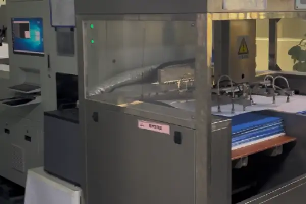
Therefore, I believe that rather than focusing our entire attention on flashy, eye-catching new features, we would be better served by gaining a deeper understanding of the foundational technologies that underpin those features—specifically, the design and manufacturing processes of PCBs. These seemingly inconspicuous elements are, in fact, often the critical factors that determine the overall quality and performance of a product. For example, within the battery management systems of electric vehicles, PCBs are responsible for monitoring the status of every individual battery cell; the precision of their design directly impacts both the safety and the efficiency of the entire battery pack. If the PCB layout is flawed or executed improperly, it can lead to uneven heat distribution or erroneous signal readings—issues that could ultimately trigger system malfunctions. Consequently, engineers utilize simulation software to optimize routing, ensuring uniform current distribution, and employ high-temperature-resistant materials to withstand the thermal environment generated during battery operation.
Of course, this does not imply that every product requires the most cutting-edge technology; rather, the appropriate design solution should be selected based on actual requirements. Sometimes, an overly complex design can actually increase costs and failure rates—a case of diminishing returns. For instance, for simple household appliances like electric fans or desk lamps, a single-layer or double-layer PCB is entirely sufficient, as their functions are singular and do not necessitate high-speed signal processing. Forcing the use of HDI or multi-layer boards would not only drive up production costs but could also introduce unnecessary complexity, thereby increasing the defect rate during manufacturing. Therefore, designers must strike a balance between performance and cost, opting for the most economically viable solution.
All in all, I believe that technological advancement should be driven by the need to solve practical problems, rather than by a blind pursuit of parametric breakthroughs. For the PCB industry, the true focus for the future should likely lie in how to better balance performance, cost, and reliability. After all, no matter how advanced a technology may be, if it cannot be widely adopted and applied, its actual value is significantly diminished—don’t you agree?
I recently had conversations with several friends in the circuit board industry and noticed a rather interesting phenomenon. Nowadays, people get incredibly excited whenever the topic of HDI PCB applications comes up. It seems as though the entire industry is scrambling to push in this direction. However, I suspect this trend may be becoming a bit overheated.
The reality I’ve observed is that many companies do not actually require such high-end technology. Everyone seems to be chasing narrower line widths and spacing, along with higher layer counts—acting as if they’ll be left behind by the times if they don’t achieve a level of 10-layer HDI or higher. But the critical question remains: does your product really require such a complex design? I’ve seen numerous projects where, in a quest for technological sophistication, teams insisted on adopting high-end HDI solutions; the result was skyrocketing costs and stagnant yield rates.
This is particularly evident now, with the AI concept being so hot; many companies feel their products will be considered obsolete if they don’t somehow incorporate an AI angle. Consequently, they rush blindly toward high-density, high-integration designs without giving it proper thought. This mindset is actually quite dangerous.
I recall a friend who works on industrial control equipment; originally, a standard four-layer board was perfectly adequate for their needs. However, they were eventually persuaded by a supplier to switch to an eight-layer HDI board. The cost nearly doubled, yet the performance improvement was negligible—so subtle, in fact, that the end users couldn’t perceive any difference whatsoever.
This brings me back to a more fundamental question: are we placing too much blind faith in technical specifications? The constantly evolving figures regarding layer counts and line widths are indeed captivating; however, the key to commercial success often lies not in the sheer sophistication of the technology employed, but rather in identifying the optimal intersection between that technology and the market.
Of course, I am not suggesting that high-end HDI lacks value. In specific domains that genuinely demand high-performance computing—such as specialized scientific computing equipment or high-end communication base stations—these advanced technologies do indeed deliver a qualitative leap in capability.
Yet, for the vast majority of consumer electronics and industrial applications, striking the right balance remains the paramount consideration.
I believe the industry currently requires a more measured and rational approach, rather than a relentless pursuit of breakthroughs in technical specifications. We should frequently ask ourselves: What level of performance does this product truly require? Which specific features are users actually willing to pay for? We must avoid blindly following trends.
After all, superior technology should serve the product—not the other way around, where the product is forced to compromise merely to accommodate the technology.
When everyone else is racing headlong in a single direction, perhaps pausing to reflect on whether that path is truly the right fit for you is the wiser choice. The same principle applies to HDI technology: its true value lies not in how advanced it is, but in how appropriately it is applied. This is where the true wisdom of designers and decision-makers is put to the test.
I feel that HDI technology has recently been somewhat overhyped—portrayed almost as a mystical necessity, as if any product failing to incorporate it is inherently obsolete. In reality, the collective rush toward high-end HDI solutions is often driven more by technological anxiety or a herd mentality than by the actual, practical requirements of the product itself.
I have encountered numerous project teams that, right from the outset, set their technical specifications excessively high. They operate under the assumption that since their competitors are utilizing third-order or even “any-layer interconnect” technologies, they must follow suit to remain competitive. The result? Not only does the manufacturing cost of the PCB board more than double, but the production yield rates also remain stubbornly low. Upon closer subsequent analysis, they discover that the pin pitch on the board’s critical chips is actually quite generous; a first-order or second-order HDI solution would have been entirely sufficient. Those superfluous layers and micro-vias turn out to be nothing more than a waste of money.
This brings to mind a fascinating phenomenon: when we discuss technology, we tend to focus exclusively on its “height”—that is, the extremes of its capability (e.g., how fine a line width or how small a via diameter can be achieved)—while rarely pausing to consider its “suitability.” The true value of a technology should not be judged solely by its level of advancement, but rather by the specific context in which it is deployed—and whether it fits that context with absolute precision. For instance, on the mainboards of consumer headphones or smart wristbands, adopting an ultra-fine, 8-layer “any-layer” HDI structure might yield negligible marginal benefits; conversely, the increased processing complexity could lead to extended production cycles and a higher number of potential failure points. The concept of “technological appropriateness” demands that engineers possess a deep understanding of the delicate balance between signal integrity, power integrity, and physical space constraints—rather than blindly stacking up technical specifications.
Take supplier selection, for example: many people place excessive emphasis on impressive-sounding equipment lists—such as whether a facility possesses the latest laser drilling machines or advanced plating lines. While these assets are certainly important, I believe it is far more critical to assess whether a factory truly understands your product requirements—specifically, whether they are willing to sit down with you to analyze which areas can be simplified and which demand absolute precision. For instance, ground vias within an RF module might require strictly controlled-depth drilling and via-filling plating to ensure impedance continuity; conversely, standard power connections can often be handled using more cost-effective mechanical drilling methods. Such differentiated process recommendations—tailored to specific functional zones—can significantly optimize the overall cost structure.
I once collaborated with an excellent supplier whose engineers would proactively suggest switching to lower-cost through-hole processes in certain non-critical areas, rather than merely pushing their high-end capabilities. This customer-centric mindset—prioritizing the client’s perspective—is far more reliable than simply showcasing technical specifications. They once shared a case study: by converting certain blind vias on a consumer electronics mainboard into buried vias—and simultaneously optimizing the stack-up sequence—they not only met all performance benchmarks but also boosted material utilization by 15% and reduced the cost per board by nearly 20%. This level of deep collaboration stems from the supplier’s thorough mastery of their own process library and their alignment with the client’s commercial objectives.
As for quality systems, it seems everyone nowadays is quick to cite ISO 16949 or ISO 13485 certifications, as if possessing such a certificate were a panacea for all potential issues. In reality, certification merely serves as an entry-level threshold; what truly determines the longevity of a partnership is a supplier’s day-to-day quality control habits and the speed with which they respond to problems. I recall an instance where we encountered a batch-wide soldering defect: the large-scale manufacturer—despite holding every conceivable certification—responded sluggishly; in contrast, a slightly smaller firm—distinguished by its strong engineering-centric culture—dispatched a team overnight to assist us in troubleshooting, and together, we quickly pinpointed the root cause. The root cause of the issue was a minute drift in a specific parameter of the electroplating solution. The factory not only rectified the problem immediately but also proactively upgraded its online monitoring system and incorporated this incident into its internal training curriculum to prevent recurrence. This organizational culture—one that views problems as opportunities for improvement—offers a far more robust guarantee of supply chain resilience than any mere certification document.
Therefore, my view is that when facing complex technical procurement decisions—such as those involving HDI PCB applications—decision-makers must establish a multi-dimensional evaluation framework. Within this framework, technical sophistication constitutes just one dimension; equally critical are cost-effectiveness, supply stability, and the fluidity of collaboration. At times, sacrificing all other aspects merely to chase a marginal gain in performance proves to be a truly counterproductive endeavor. For instance, in the realm of automotive electronics, factors such as long-term supply assurance for a technical solution, reliability data under extreme temperature conditions, and the rigor of change management processes may carry far greater weight than mere specifications regarding line width and hole diameter. An effective framework should be capable of dynamically adjusting the priority assigned to these various dimensions based on the product’s lifecycle, market positioning, and risk tolerance.
The pace of iteration in modern electronic products is incredibly rapid; what constitutes a high-end configuration today may well become the standard mid-range specification by next year. In such an environment, selecting a technical solution that is “just sufficient yet stable and reliable” is often a wiser strategy—and one more conducive to project success—than opting for the “most advanced” solution available. Ultimately, technology exists to serve the product—not the other way around, where the product is forced to contort itself to accommodate the technology. This “philosophy of sufficiency” demands that teams possess the capability to define requirements with precision and maintain deep insight into technological roadmaps. By avoiding being swayed by flashy marketing jargon, they can focus their resources and attention squarely on the core innovations that genuinely create value for the end user.
I have long felt that many people’s understanding of HDI is somewhat misguided. People tend to fixate on technical specifications—such as the number of layers, line widths, and spacing—and while these details are certainly important, they are rarely the factors that ultimately determine a project’s success or failure. What truly matters is the reliability of the partners you choose to work with. I have seen far too many teams whose designs look spectacular on paper, only to find themselves completely stalled and unable to move forward once they hit bottlenecks with their suppliers.
Ultimately, the application landscape for HDI PCBs has long since evolved beyond the simple confines of mobile phones and computers. Nowadays, any electronic product with even the slightest ambition aims to be more compact while simultaneously packing in more functionality—a goal that makes the high-density interconnect design philosophy absolutely indispensable. From wearable devices to precision industrial controllers, and even the tiny flight control boards found in drones, this technology is being adopted on a massive scale. But herein lies the critical question: You may be able to design it, but can your partners actually manufacture it? This is precisely why selecting the right supplier has become such a pivotal factor.
In my own experience, you shouldn’t simply take a supplier’s word for how cutting-edge their equipment is. You need to go and see for yourself whether their production lines truly operate smoothly, and—more importantly—whether their engineering team possesses the capability to resolve unforeseen issues on the fly. For instance, we once had a board design that required a specialized blind and buried via configuration; several suppliers claimed they could handle it. In the end, however, only one supplier actually sat down with us to analyze how material properties would impact signal integrity, and then adjusted the stack-up scheme accordingly to achieve a viable solution. You must be especially wary of those suppliers who merely nod and say, “Yes, we can do that”; they are often the ones who will saddle you with a host of unexpected headaches once mass production begins.
Therefore, rather than obsessing over the numbers listed in technical data sheets, you would be better served by dedicating more time to evaluating your suppliers. How responsive are they? How cooperative are they when faced with design changes? Do they possess sufficient technical reserves to accommodate your potential future requirements and upgrades? These “soft capabilities” often reveal far more about a partner’s true worth than any rigid technical metric ever could.
After all, the inherent complexity of the HDI process dictates that it cannot be treated as a mere “outsourced” task to be simply offloaded and forgotten. It demands a tight, seamless integration between the design and manufacturing ends, with both parties working in lockstep to drive the project forward. Finding a partner willing to tackle the toughest challenges alongside you is infinitely more valuable than simply finding a fabrication plant that offers the lowest quote. While this may sound like common sense, in the heat of actual project execution—often driven by tight deadlines—we frequently overlook this fundamental truth.
BMS reliability isn’t decided by algorithms — it’s decided by the PCB
Beamforming performance depends on phase coherence across every antenna element — and
A relay control board that works perfectly in the lab can fail
- Pienten ja keskisuurten erien tuotannon asiantuntija
- Korkean tarkkuuden piirilevyjen valmistus ja automatisoitu kokoonpano
- Luotettava kumppani OEM/ODM elektroniikkaprojekteihin
Aukioloajat: (ma-la) klo 9:00-18:30.