
Industrial Automation PCB Reliability: How to Achieve 10+ Years of Stable Operation
In the field of industrial automation, people often pay attention to AI
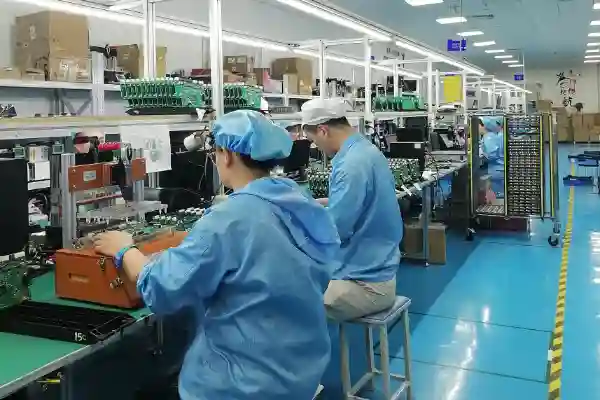
I recently chatted with a friend who works in smart hardware and discovered an interesting phenomenon—their team’s new product, developed over six months, stumbled during small-batch trial production. Where did the problem lie? A sensor on the circuit board kept malfunctioning inexplicably. Upon investigation, it was discovered that a worker at the contract manufacturer was handling it with bare hands without wearing an anti-static wrist strap.
This incident reminded me of a common pitfall for many startups: focusing solely on the glamorous aspects like chip selection or software algorithms. In reality, the true determinants of product stability are often the devil in the details—such as the fundamentally basic and easily overlooked aspect of electrostatic discharge (ESD) protection during PCB-kokoonpano.
When choosing PCBA suppliers, I pay particular attention to the details of their workshop management. During a visit to a PCB assembly factory in Shenzhen, I noticed an interesting contrast: Factory A’s showroom was filled with brochures about high-speed placement machines but vaguely addressed ESD measures; Factory B’s reception area had a real-time ESD monitoring screen on the wall, and even provided conductive shoe covers for visitors. Ultimately, we chose the latter, and in three years of cooperation, we haven’t experienced any batch quality issues.
Now, some clients strive to cram in as much functionality as possible, wanting to achieve supercomputer performance on a board the size of a fingernail. However, the heat dissipation and stress issues brought about by high-density packaging have become its Achilles’ heel. I handled a smart wearable project where the blind pursuit of thinness led to a surge in chip solder joint defects, ultimately forcing a return to a more robust packaging solution.
A good PCBA partner should be like a traditional Chinese medicine practitioner, focusing on systemic treatment rather than simply addressing the symptoms. Last week, a medical device company contacted me to recommend PCB assembly services. I specifically reminded them to pay attention to whether the foundry has a complete reliability testing process; after all, medical product failures can be life-threatening, which is far more important than simply comparing prices.
Ultimately, the electronics manufacturing industry is undergoing a transformation from extensive to intensive production. Ten years ago, a few secondhand machines might have been enough to start a PCBA workshop; now, without a comprehensive quality management system, it’s impossible to secure high-quality orders. This reshuffling is actually beneficial for companies that are serious about product development.
I’ve been pondering something lately: why are more and more companies willing to outsource the entire PCB assembly process? It’s not just about finding a foundry to solder a few components. A few days ago, I was chatting with a friend who works in smart hardware and discovered that their team doesn’t even have a single engineer who understands soldering; all PCBA production is outsourced to professional suppliers. This made me realize that the way electronics manufacturing works has truly changed.
In the past, owning your own production line was considered a symbol of strength, but that idea seems outdated. Today’s PCBA suppliers offer far more than basic assembly; they handle the entire process from design optimization and component procurement to post-production testing. You just need to state your requirements. This shift reflects a deepening of specialization. After all, electronic components are getting smaller and the manufacturing requirements are becoming increasingly stringent. Building your own production line is not only expensive but also requires constant technological updates; it’s better to delegate to more specialized professionals.
I’ve seen some startups initially try to save money by tinkering with PCBs themselves, only to have entire batches of products reworked due to substandard soldering, delaying their market launch. Later, they found a reliable PCB assembly manufacturer, which not only solved the quality issues but also reduced costs through bulk component procurement. This shows that choosing a good PCBA service is not just about saving time but also about mitigating risks.
Another interesting phenomenon is that PCBA suppliers are now acting as technical consultants. For example, before assembly, they will review your design documents and point out areas that might affect mass production efficiency. This advice is invaluable for design teams lacking manufacturing experience. After all, no matter how perfect the circuitry on the blueprints is, it’s useless if problems keep arising during actual assembly.
Of course, outsourcing doesn’t mean abandoning responsibility. You need to understand the required level of craftsmanship for your product. For example, ordinary consumer electronics may not have such high requirements for soldering precision, but industrial or medical equipment requires manufacturers with strict quality control processes. This is why there are so many different levels of PCB assembly services on the market; some specialize in small-batch rapid prototyping, while others excel in large-scale standardized production.
I think this division of labor will become increasingly common in the future, especially with the rise of the Internet of Things and smart hardware. Many teams’ core competencies are software and user experience, while hardware manufacturing has become a non-core aspect. Finding the right partner can help your product reach the market faster and, more importantly, make it more reliable, wouldn’t you agree?
I’ve seen many teams make the same mistake when choosing PCB assembly services—they always focus on the numbers on the quote. In fact, what truly affects the success or failure of a project are those easily overlooked details. For example, last week a client making medical equipment suddenly discovered that the yield rate dropped sharply during mass production. Upon investigation, it turned out to be due to batch differences in the flux used in the soldering process. These variables, hidden deep within the supply chain, often only become apparent after the product launch.
Finding a PCBA supplier is increasingly like solving a multi-dimensional puzzle. Simply looking at equipment parameters is no longer enough; you need to see how they handle unexpected situations. One PCB assembly manufacturer we worked with last year left a deep impression. When a key chip was in global shortage, they coordinated three alternative solutions within 48 hours and even redesigned hot air pads compatible with different packages.
Many people think that simply handing over documents to the factory is enough, but the process from design to mass production requires continuous communication. Especially as board density increases, those 01005 packaged components are the ultimate test of the precision of the placement machine. The most dramatic experience I’ve had was when a batch of BGAs had cold solder joints, which turned out to be due to a malfunction in the workshop’s temperature and humidity logger. These seemingly insignificant details are often the dividing line between high-quality PCBAs and ordinary assembly.
The pace of electronic product iteration is too fast now; sometimes, small-batch trial production doesn’t even wait for complete reliability testing. At this point, the supplier’s rapid response capability is crucial. A good PCB assembly service provider should act like a seasoned navigator, able to anticipate technical risks and flexibly adjust process routes. For example, recently we tried to integrate the RF module and main controller onto the same board, and the manufacturer suggested using a stepped stencil to solve the solder paste printing problem for different pin pitches.
Ultimately, PCA (Printed Circuit Assembly) isn’t simply about gluing components onto a board; it’s about ensuring that thousands of solder joints can function stably for years to come. This requires the assembler to have an almost obsessive control over material properties, process parameters, and equipment status. Sometimes, seeing solder joints that remain shiny and clean after undergoing high and low temperature cycling tests makes you realize that this industry truly requires a craftsman’s spirit.
I recently chatted with some friends in the hardware industry and discovered a rather interesting phenomenon—many people now only focus on the high-end, fully automated equipment when they talk about PCB assembly. However, from our actual production perspective, the problems often lie in the most basic steps.
I remember last year a customer came to us with design drawings for small-batch trial production. The board itself was quite complex, using a large number of micro-components and several special-sized through-hole structures. After the first batch of samples came out, it was discovered that some component leads weren’t fully tinned. After considerable investigation, it was found that the solder paste’s fluidity had changed due to insufficient settling time after mixing. Such details are often not explicitly noted in the standard procedures of PCB assembly manufacturers, but they precisely determine the reliability of the final product.
When choosing PCB assembly services, many people easily fall into a misconception—overly pursuing placement speed. In reality, for most small-to-medium batch projects, the component pre-processing stage is more important. For example, chips sourced from different channels may have different pin oxidation levels. If all are reflow soldered using the same oven temperature profile, it can result in poor solder joints or even require rework of the entire batch.
While through-hole technology is becoming increasingly rare, it remains irreplaceable in certain scenarios. We previously worked on a batch of industrial control boards that required the installation of high-power relays. A simple surface-mount structure couldn’t withstand long-term vibration, so we ultimately chose a through-hole solution combined with wave soldering. A good PCB OEM supplier should be able to flexibly combine different processes based on the actual application scenario, rather than simply recommending the so-called latest equipment.
During a visit to a partner’s workshop, I noticed their quality inspectors randomly checked finished PCBs with magnifying glasses, meticulously examining the solder paste’s condition. This seemingly primitive method is actually more effective at identifying potential problems than simply relying on 3D inspection equipment. After all, machines can only judge geometric dimensions, while experienced technicians can discern subtle differences in solder paste gloss.
Ultimately, PCB assembly isn’t just about piling on the latest technologies to create a good product. Every step requires experience. Like cooking, it’s not just about the stove’s heat, but also about mastering the order and timing of adding ingredients. This is the fundamental difference between a reliable PCB assembly manufacturer and an ordinary processing plant.
Over the years in PCB assembly, I’ve found that many people overcomplicate things. Finding the right PCB assembly manufacturer is more important than anything else, just like finding a skilled hairdresser—a good one saves you a lot of trouble. When I first started in PCB assembly services, I was always fixated on how advanced the equipment needed to be. Later, I realized that what truly affects the final product are the details.
For example, the design of the stencil openings is particularly important. Once, we were making a batch of boards with BGA chips, and the stencil provided by the supplier had the wrong aperture ratio, resulting in severe solder joint defects. I still remember the scene of the experienced worker painstakingly scraping away the solder paste with a magnifying glass during rework. Therefore, now when choosing a PCBA supplier, I always ask how they verify the process of their stencils. In fact, a professional verification process includes using laser cutting to measure the aperture, and also using 3D optical inspection to confirm the aperture taper and wall surface finish. Some high-end manufacturers even use simulation software to simulate the solder paste flow process to ensure that ideal solder joint shapes are formed during high-temperature reflow. Although this early verification increases costs, it can avoid catastrophic soldering defects during mass production.
Component placement is also an art. I’ve seen some manufacturers place surface-mount capacitors too close together to save space, resulting in solder balls flying everywhere during reflow soldering. Good PCB assembly services should know how to find a balance between density and reliability, rather than blindly pursuing miniaturization. A reasonable layout should consider the balanced distribution of heat capacity; for example, heat dissipation space should be reserved around high-power devices, and long parallel traces should be avoided for high-frequency signal paths. Experienced engineers will install solder mask bridges between components and employ solder-skimming pad designs in wave soldering processes; these details can significantly improve soldering yield.
A recent project gave me a new understanding of solder paste selection. It turns out that different brands of solder paste perform very differently at high temperatures, especially when using lead-free processes. One manufacturer I’ve worked with prepares two or three types of solder paste for different component types, using them like a chef seasoning dishes—this level of attention to detail is truly reassuring. For example, they use No. 5 powder solder paste for fine-pitch QFP chips to ensure printing accuracy, while No. 3 powder is used for large pads like those on heatsinks to increase solder paste deposition. They also select solder pastes with different activators based on the product’s operating environment; highly active solder paste is used for automotive electronics to cope with harsh environments, while medium-active paste is used for consumer electronics to control costs.
In fact, the most direct way to judge the reliability of a PCBA supplier is by how they handle abnormal situations. Once, we had an urgent redesign that required adjusting the stencil openings overnight. A reputable manufacturer would remake the stencil, while some small workshops might simply modify it manually. This difference directly affects the yield rate in mass production. Professional emergency response involves first creating a temporary laser stencil, then initiating the regular electroformed stencil production process, and increasing the frequency of X-ray inspections during the first-piece inspection. This systematic approach ensures both on-time delivery and consistent quality.
I now value a manufacturer’s understanding of the process more than the length of their equipment list. I’ve seen people use the latest pick-and-place machines but still misplace 0402 components, and I’ve seen experienced craftsmen use older machines to produce precision medical equipment. Ultimately, PCB assembly is a craft that requires accumulated experience. Truly knowledgeable engineers adjust the placement pressure based on the board thickness, set up special support fixtures for flexible boards, and can even judge nozzle wear by listening to the sound of the pick-and-place machine. This kind of experience gained through practice is far more valuable than the numbers on equipment parameter sheets.
I remember once visiting a factory and seeing them give QFN components special treatment, using a stepped design on the stencil to increase solder paste volume. This targeted solution is much more practical than vague talk of “advanced processes.” This stepped stencil thickens the ground pad area by 0.1mm, ensuring good heat dissipation while preventing chip floating. They also developed a custom reflow profile for QFN, setting a longer preheating time before the melting point to fully activate the flux. This customized process reduced the cold solder joint rate of QFN from the industry average of 3% to below 0.5%.
Now, every time I inspect samples, I pay special attention to the full and smooth solder joint shape. Behind these solder joints often lies the accumulation of mature process parameters. Finding a PCB assembly manufacturer with whom you can cooperate long-term can indeed make product development much more efficient.
Every time I see those circuit boards densely packed with components, I think about how behind them lies a sophisticated collaborative system. Many people think that finding a PCB assembly manufacturer is simply throwing in the blueprints and waiting for the finished product. But in reality, the entire PCBA process is more like solving a 3D jigsaw puzzle; every step tests the supplier’s comprehensive capabilities.
I’ve seen many startups focus on circuit design but neglect the seemingly simple step of component procurement. Sometimes, a small, inconspicuous resistor can stall the entire production schedule. The strength of a reliable PCB assembly service provider lies not in how advanced their equipment is, but in their ability to quickly mobilize resources and assemble components scattered around the world like building blocks on time. It’s far more important than simply comparing prices.
Once, we had a project that required chips with specific packages. All the major PCBA suppliers showed stock shortages, but a manufacturer we’d worked with for years resolved the issue within 48 hours using alternative solutions. They even anticipated the impending discontinuation of certain components and proactively offered alternatives. This risk management capability hidden behind the process is the truly valuable aspect.
Many people fall into the trap of comparing equipment specifications when choosing partners. However, what truly affects the quality of the finished product are the unseen details, such as temperature and humidity control in the workshop, the degree to which employees implement ESD protection, and even batch management on the material racks. These daily operational procedures are often more reliable than the technical specifications in brochures.
Ultimately, PCB assembly isn’t a standardized assembly line operation. Every project presents new challenges. Good partners will work with you to adjust soldering temperature profiles, optimize component layout and spacing, and even provide design improvement suggestions based on actual assembly conditions. This dynamic adjustment capability is far more important than simply producing according to blueprints. After all, circuit boards ultimately need to operate in various environments over the long term; theoretical data can never replace the experience accumulated through actual assembly.
Every time I see those complex circuit boards running in my hands, I think that PCB assembly is far more than just a technical job. I’ve seen too many people focus entirely on equipment parameters, neglecting the unseen details that truly determine success or failure. For example, when choosing a PCB assembly manufacturer, many people focus on the price, but the real question should be how they handle those tiny solder joint issues. An excellent PCBA supplier should be like a skilled traditional Chinese medicine practitioner taking a pulse, able to anticipate potential problems.
I remember a project we had last year where several inconspicuous cold solder joints appeared after reflow soldering. Some in the team suggested moving directly to the next stage, but I insisted on stopping to re-inspect the solder joint condition. The problem turned out to be a solder paste activity issue—a hidden danger that, if left until the functional testing phase, could render the entire batch of boards unusable. This incident reinforced my belief that the most crucial aspects of PCB assembly are often the most easily overlooked.
Many manufacturers like to boast about their automation levels, but when rework is truly needed, it still comes down to the skill of experienced technicians. The most reliable suppliers I’ve worked with have quality inspectors who can judge the soldering status of BGA packages by touch. This accumulated experience is more reliable than any testing equipment; after all, X-ray machines can only see the shape of the solder balls, while experienced technicians can sense the potential impact of thermal stress on components.
Recently, a client asked me why the same design documents yielded such significant differences between different manufacturers. The answer lies in the everyday details—some manufacturers treat testing as a separate process, while others integrate testing principles throughout the entire production flow. For example, they consider the possibility of future rework and leave room for adjustments before surface mount technology (SMT), or they calculate the relationship between solder paste thickness and component heat capacity when designing the stencil.
Sometimes, seeing newly hired engineers struggling with test reports reminds me of my own early days in PCB assembly. Back then, I always thought that as long as we followed the standard procedures, nothing would go wrong. Later, I realized that truly good products often arise from thinking beyond the standards. Like when handling double-sided mixed-assembly boards…
I’ve always felt that the most fascinating part of PCB manufacturing isn’t the design phase, but the post-processing stage. Many people focus on wiring layout but neglect the processes that truly determine the product’s lifespan. Take the industrial controller we made last year, for example. The three-proof coating alone required three reworks—the first time the coating thickness wasn’t up to standard, the second time we found a corner wasn’t covered, and only on the third time did it pass the salt spray test. These kinds of details often test the PCB assembly manufacturer’s professionalism more than the circuit design itself.
Now, many PCB assembly service providers are promoting flexible board processing, but few truly master rigid-flex board technology. I’ve seen manufacturers use ordinary reflow soldering profiles to process polyimide substrates, resulting in the entire batch of boards bubbling and deforming. The sintering temperature window for flexible boards is extremely narrow; a 5-degree increase will cause the material to curl, while a 5-degree decrease may lead to poor soldering. This kind of delicate work requires production line workers to have an almost intuitive grasp of the material properties.
The assembly of high-power modules is even more of a science. After two years of continuous operation at 150 degrees Celsius, traditional solder paste showed signs of whisker growth upon disassembly and inspection. Switching to eutectic solder in a nitrogen-protected furnace doubled the cost, but the thermal fatigue test results were significantly better. Recently, we’ve been testing a nano-silver paste sintering process; its thermal conductivity is indeed close to pure silver, but the pressure control precision is extremely high. Even slight vibrations in the workshop can affect the connection strength.
I was once impressed by the underfill process of an automotive electronics PCBA supplier. It wasn’t just simple dispensing; they meticulously inspected the adhesive layer height under a 40x microscope, requiring rework even for deviations as small as 0.1 millimeters. The manager explained that this was a lesson learned the hard way – years ago, a batch of automotive radar chips detached after 5,000 thermal cycles due to uneven adhesive thickness, leading to a large-scale recall.
These specialized processes truly test overall teamwork. Last week, a project involving both eutectic soldering and flexible board mounting required three meetings between the engineering and production departments just to coordinate the temperature profiles of the two processes. The final compromise was to partially shield the flexible board portion first, and then process the flexible area separately after the mainboard completes its high-temperature process. This ability to adapt flexibly is key to judging the quality of PCB assembly.
I firmly believe that good assembly shouldn’t be seen as a standardized process, but rather as a creative process imbued with craftsmanship. Just as a master craftsman can judge the density of a sintered silver layer by its reflection, some experience simply can’t be written into the work instructions. This is why similar equipment produced by different manufacturers yielded products with completely different reliability—machines are merely tools; the true essence of craftsmanship lies in human judgment.
I’ve seen many people obsess over superficial factors like price or delivery time when choosing PCB assembly services. In reality, the key to whether a board can operate stably for ten years often lies hidden in those seemingly insignificant process details.
I remember last year we had a project where we partnered with a new PCBA supplier. Their promotional materials were very attractive, and their prices were very competitive. However, the first batch of samples had problems. The boards developed cold solder joints in less than 48 hours of operation under high temperatures. Upon inspection, we discovered that their soldering temperature profiles were completely unsuitable for our components.
This experience made me realize that judging a PCB assembly manufacturer shouldn’t just be about the hardware they showcase; it’s more important to assess their depth of understanding of the processes. Good manufacturers will proactively discuss temperature parameters, solder paste selection, and even cleaning agent residue standards for each step. These seemingly trivial details precisely determine the reliability of the final product.
Now, before collaborating with a new PCB assembly manufacturer, I always ask them how they control the reflow soldering temperature rise rate and monitor solder paste thickness fluctuations. The answers often reflect whether they mechanically execute standards or truly understand the physical principles behind the process.
Once, during a visit to a top-tier automotive electronics PCBA workshop, I noticed that they had color-printed error-prevention reminders at every workstation. Even screws and torque wrenches were color-coded according to different specifications. This attention to detail is worthy of products with high reliability requirements.
In fact, there’s a very intuitive way to judge a supplier’s level—observe their reaction to problems. Do they rush to shirk responsibility or quickly organize engineers to analyze the root cause? The latter often indicates a continuous improvement capability, which is more valuable than any certification.
Recently, we’ve started collaborating with suppliers on data traceability systems for medical equipment projects. This not only records production batches but also links them to the temperature, humidity, and equipment status parameters in the workshop at the time. This transparent collaboration gives both parties greater confidence in the reliability of the final product.
Ultimately, good PCB assembly services should be a partnership, not just a simple client-supplier relationship. When suppliers are willing to spend time understanding your product’s application scenario and proactively share suggestions for process improvement, price becomes a secondary consideration. After all, nobody wants to gamble the success or failure of the entire project to save a few dollars.
In the field of industrial automation, people often pay attention to AI
Ever wonder how your phone maintains a stable signal? It relies on
When selecting components for a security monitoring system, most attention goes to
- Pienten ja keskisuurten erien tuotannon asiantuntija
- Korkean tarkkuuden piirilevyjen valmistus ja automatisoitu kokoonpano
- Luotettava kumppani OEM/ODM elektroniikkaprojekteihin
Aukioloajat: (ma-la) klo 9:00-18:30.