
Why the Circuit Board Beneath the Camera Determines Whether Your Surveillance System Holds Up for Years
When selecting components for a security monitoring system, most attention goes to
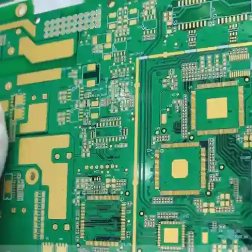
Recently, our engineers noticed an interesting phenomenon while debugging a high-frequency circuit board in the lab – many people’s understanding of high-end PCB materials is still limited to the parameter sheet level. That day, he told me that he was testing a millimeter-wave radar module using Rogers materials and found that even with substrates of the same nominal parameters, there were subtle differences in signal integrity performance across different batches. This difference often manifests as subtle variations in phase noise and insertion loss, especially in the frequency range above 28GHz. For example, a certain batch of boards showed an additional 0.2dB of loss at 77GHz; although the value is small, it can become a critical problem when the system link budget is tight. After in-depth analysis, we found that this fluctuation mainly stems from microscopic differences in the glass fiber weave density of the substrate, which leads to local changes in the propagation speed of electromagnetic waves.
This reminded me of a 5G base station project I participated in three years ago. At that time, the team tried various solutions to reduce signal loss, but ultimately found that the key to the problem was not in the quality grade of the Rogers PCB material itself – although we did choose a low-loss model – but in the process control during manufacturing. During a visit to the contract manufacturer, I noticed a detail: their temperature and humidity control in the workshop was relatively lax when handling ordinary FR4 materials. However, for high-frequency materials, a change in environmental humidity exceeding 10% can affect the moisture absorption rate of the dielectric layer, thereby changing the dielectric constant of the material. Even more noteworthy is the drilling process. When using ordinary tungsten carbide drill bits to process high-frequency circuit boards, the hole wall roughness can reach 18μm, while drill bits with special coatings can control the roughness to within 8μm, which is crucial for reducing signal reflection.
In fact, many people tend to overlook the symbiotic relationship between material properties and manufacturing processes. Take the coefficient of thermal expansion, for example. Laboratory data does show that certain models have excellent thermal stability, but in practical applications, we found that when manufacturing temperature fluctuations exceed a critical value, even the best materials will experience delamination, especially in designs requiring embedded components, where the lamination process requirements are even more stringent. For example, during multiple lamination processes, if the heating rate exceeds 3℃/second, some ceramic-filled materials will develop microcracks. These cracks gradually expand during thermal cycling tests, ultimately leading to interconnect reliability problems. We observed with a thermal imager that improper lamination parameters can cause local temperature differences in the board material of up to 15℃, which is enough to cause a 0.5% dimensional variation in the Z-axis direction.
I remember once helping a friend troubleshoot a car radar module. After disassembly, we found that although it was a standard 77GHz application scenario, the copper foil treatment on the board surface clearly did not meet the requirements for high-frequency signal transmission. Later, using a version with special surface treatment solved the problem. This incident made me deeply understand that the right materials need to be matched with corresponding manufacturing standards. In that case, the surface roughness of ordinary rolled copper foil reached 0.5μm, while high-frequency applications require reverse copper foil technology to reduce the roughness to below 0.2μm. More importantly, the control of copper foil crystal orientation is crucial; an ideal 110 crystal orientation ratio needs to reach over 85% to ensure minimal skin effect loss for high-frequency signals.
Now, when dealing with high-frequency projects, I pay more attention to whether the contract manufacturer has production lines specifically for handling special materials. Their cleanroom class is not the only indicator; the key is whether the operators understand the characteristics of these materials. For example, some engineers habitually use FR4 processing parameters to process ceramic-filled materials, which actually destroys the original performance advantages of the material. We have established an evaluation system that focuses on assessing the manufacturer’s understanding of material pretreatment. For example, high-frequency laminates need to be left to stand for more than 48 hours under specific temperature and humidity conditions before cutting, but many factories often ignore this step to meet deadlines. In addition, the energy parameters of laser drilling need to be dynamically adjusted according to the ceramic content in the material; the 20W laser power commonly used for ordinary FR4 materials will lead to excessive carbonization when processing boards with high ceramic content.
In a recent satellite communication project, we tried an innovative approach of mixing and stacking different types of materials. This method is not found in official documentation, but by adjusting the combination of dielectric thicknesses, we unexpectedly achieved better results in specific frequency bands. This perhaps illustrates that there is always room for exploration in the application of high-end materials. We mixed RO4350B and RO3003, and by precisely controlling the thickness ratio of different dielectric layers, we achieved a flatter phase response in the Ku band than with a single material. The key to this mixed structure lies in the interface treatment technology. We used a special plasma activation process to create a molecular-level bond between the different dielectric layers, controlling interface loss to below 0.05dB. Even more surprisingly, this mixed stacking structure exhibited better thermomechanical stability; the dimensional change rate was reduced by 30% compared to a single material during temperature cycling from -55℃ to 125℃.
In my years of experience in RF design, I’ve noticed that many people instinctively think of specific brands of high-end materials when it comes to high-frequency circuits. However, choosing a laminate is like choosing ingredients; more expensive isn’t always better. The key is to consider what characteristics your recipe requires.
I’ve seen many teams blindly pursue branded laminates, resulting in doubled costs. High-frequency design does indeed have stringent requirements for stability. Once, when testing the temperature adaptability of different materials, we found that some ordinary laminates performed well at room temperature but showed significant signal drift with temperature fluctuations. This highlights the importance of dielectric constant stability.
What truly affects high-frequency performance is often not the brand of the material, but the consistency of its internal structure. For example, when electromagnetic waves pass through a dielectric, if the material density is uneven, phase noise will be generated. This reminds me of a radar module I debugged earlier. Initially, to save costs, we chose a medium-priced laminate, but it resulted in resonance in the millimeter-wave band. The problem was only solved by switching to a material with ceramic filling characteristics.
What many people tend to overlook is the difference in processing techniques for high-frequency laminates. Once, we tried to directly apply the standard FR-4 production process to special materials, which resulted in microbubbles during the lamination process. Later, we realized that these materials require a specific hot-pressing curve, just like baking requires precise control of oven temperature.
Now, we’re seeing more and more domestically produced high-frequency materials emerging. There’s no need to be fixated on imported brands; the key is to establish our own testing database. Recently, in a 5G base station project, we used ceramic substrate materials developed by a local manufacturer. Not only did it reduce costs by 30%, but the dielectric loss tangent in humid and hot environments exceeded expectations.
What’s truly important is understanding the nature of the interaction between electromagnetic waves and the dielectric material, not blindly worshipping a particular brand name. Whenever I design a new product, I ask my team to first define the frequency boundaries of the application scenario and then work backward to determine the required material parameters. This often leads to more optimized solutions.
I’ve always found the field of high-frequency circuit boards particularly interesting. Many people may not realize that choosing Rogers PCB materials is actually a balancing act. Professional-grade boards do provide better signal integrity, but this doesn’t mean that all scenarios require the highest specifications.
I remember once helping a client with antenna design, and we tried different specifications of Rogers materials. Some projects are very cost-sensitive, so we had to find the best balance between performance and budget. Sometimes, using a slightly more common model and optimizing the layout can achieve good results. This taught me a valuable lesson: the most expensive isn’t necessarily the most suitable.
The quality of the etching process directly affects the performance of the final product. I’ve seen many cases where subtle deviations in the etching process led to the scrapping of entire batches of products. Especially when the circuit density is very high, even a small defect in a few square feet can render the entire board worthless. This kind of precision work really requires experience and patience.
I think many engineers nowadays rely too much on standard parameters. Every project has unique requirements and environmental conditions, such as temperature variations and mechanical vibration conditions, which all affect material selection. Once, we took on an industrial control project where the client initially specified a high-end Rogers material. However, after actual testing, we found that using a mid-range model was more suitable for the temperature fluctuations on-site.
Quality control is also worth discussing. I’ve seen too many people focus only on raw material certification, neglecting the details of the processing steps. The cleaning process after etching, for example, seems simple but directly affects product lifespan. One factory improved its manufacturing process by making changes to the cleaning stage, resulting in a 30% increase in the reliability of circuit boards of the same specifications.
Ultimately, choosing professional-grade high-frequency circuit boards is like choosing a partner. It’s not about how powerful it is, but whether it truly suits your project needs. Sometimes, spending a lot of money on top-of-the-line components is less effective than finding the most suitable solution. This industry requires a deep understanding of every detail, not blindly following the numbers on a specification sheet.
When selecting components for a security monitoring system, most attention goes to
Behind the mobile signals we rely on daily lies the sophisticated engineering
Many assume that wireless communication PCBs require expensive high-frequency materials. This guide
- Pienten ja keskisuurten erien tuotannon asiantuntija
- Korkean tarkkuuden piirilevyjen valmistus ja automatisoitu kokoonpano
- Luotettava kumppani OEM/ODM elektroniikkaprojekteihin
Aukioloajat: (ma-la) klo 9:00-18:30.