

Automotive Rain Sensor PCB: How Optical Paths, Potting, and Fabrication Quality Decide Field Performance
Do you think a rain sensor is just a simple circuit board?
Every time I see someone reduce the value of a PCB prototype down to simply “validating the design,” I feel that understanding is far too shallow. I’ve handled quite a few projects and noticed a pattern: a lot of people’s expectations for a prototype are overly idealistic.
You only realize where the real problems are once you actually start building. A friend in smart-home products got burned exactly this way — he assumed following the standard process would let him smoothly move into mass production.
In reality, going from the first sample to final design lock-in usually requires several rounds of adjustment.
The most extreme case I’ve seen was a team that revised their routing scheme eight times during the prototype stage before finally solving a signal-interference problem.
That kind of repeated revision process is precisely what exposes blind spots in the initial design.
Something a lot of people easily overlook is how material selection affects everything downstream.
For example, high-frequency circuits have completely different substrate requirements — the exact kind of consideration that matters enormously on a Point-to-Point Microwave Link PCB.
Sometimes, to save a little money, people choose an ordinary material, only to have the entire product line come out unstable — a false economy.
Another common misconception is over-chasing low cost and fast delivery.
Once, I saw a peer skip impedance testing to rush the schedule and go straight to small-batch production, only to have the entire batch scrapped and rebuilt.
On the surface, it looked like they saved two weeks; in reality, it delayed the entire quarter’s plan.
The genuinely reliable approach is factoring in potential mass-production process limits right at the prototyping stage.
For example, whether pad size suits automated production lines, whether trace spacing can meet existing equipment precision — these details often determine success or failure.
A recent case I came across was genuinely interesting: a startup team invited their contract manufacturer’s engineer — in this case a multilayer pcb manufacturer with deep stack-up experience — to participate in design review right at the prototype stage, proactively avoiding three potential production bottlenecks.
That kind of front-end collaboration model is worth learning from.
At the end of the day, treating a prototype as merely a “trial-and-error step” is a waste of resources — it should be the bridge connecting creativity and reality, with every revision paving the way toward scaling up.
Every time I see someone excitedly testing a freshly made PCB Prototype, I find it genuinely interesting. Actually, a lot of people easily overlook a key point — what genuinely determines a circuit board’s success or failure often isn’t those final debugging steps.
I’ve seen too many people pour all their energy into agonizing over trace width or via count. Once, helping a friend revise a drone flight-controller board, I found something interesting: he’d stacked a power layer on a four-layer board but mixed analog and digital ground together, causing sensor readings to drift. This kind of problem is completely invisible at the schematic stage — it only surfaces once the prototype comes back for testing.
Many EDA tools today are genuinely convenient, but they easily create an illusion — as if a few clicks of auto-routing solves everything. In reality, software can never replace an engineer’s understanding of current loops — for example, high-frequency signal paths need to stay as short as possible, and digital circuitry needs to stay away from analog components. These judgments require accumulated experience.
A recent project left a strong impression on me. The client insisted on compressing cost by converting a six-layer board into a four-layer one, and the first batch of samples all failed — only after readjusting component placement did it pass testing. Sometimes blindly chasing low cost actually increases the expense of downstream revisions.
The genuinely reliable approach is factoring in actual layout from the moment you draw the schematic — placing tightly related modules in adjacent areas, reserving enough debug-interface access. After all, no simulation, however perfect, compares to the reality of an actual power-on test.
I remember making a rookie mistake early in RF-circuit work — routing a clock signal right next to an antenna feed line, cutting wireless transmission distance in half. It took three times as long afterward to pinpoint the interference source. So now I’ve made it a habit: critical signal paths always get manually routed — anything auto-generated is treated as a reference at most.
At the end of the day, building a PCB Prototype is a lot like assembling building blocks — every step interlocks with the next. Spending more time optimizing layout upfront saves an enormous amount of debugging cost later. The longer you’re in this business, the more you find that the best tool is always the engineer’s own judgment.
Chatting recently with a friend about our experience building circuit boards, I noticed something genuinely interesting — a lot of people treat making PCB Prototypes as a mere compliance-check step. Actually, this is a genuinely fascinating business.
I remember how excited I was the first time I got my own designed board back. It literally started smoking the moment it was powered on. That’s when I understood that building a prototype isn’t simply turning a drawing into a physical object — it’s more like building a bridge between the virtual and real worlds.
Once, to save time, I skipped the impedance-matching check. As a result, the board completely failed to function in a high-frequency environment. That lesson made me realize every detail needs to be carefully scrutinized.
Now, seeing young engineers rush straight to mass production with their first prototype version, I always think back to how I was back then. Every trace and every via on a circuit board can hide a trap.
After doing this enough, I’ve found that what’s genuinely precious isn’t the final successful version — it’s the pile of failed test units stacked in the corner. They’re like footprints along the road to growth, recording every round of adjustment and improvement.
Sometimes, drawing on a glowing screen late at night, it suddenly hits me that these lines are about to become real copper foil and substrate. That process of creation from nothing is itself full of magic.
Recently, checking a junior schoolmate’s graduation project, I gained a new realization. He was fixated on the placement of a single component, when what actually matters more is whether the overall layout is reasonable. This kind of holistic thinking only develops through repeated practice.
Every time I get a newly sampled board, it feels like unboxing a mystery box. It might run flawlessly, or it might throw up an unexpected problem — but it’s exactly that uncertainty that makes the whole process so engaging.
I actually enjoy the early repeated-revision stage more now, because that’s where creativity genuinely shows through.
Watching soldered components glow and heat up on the board, that sense of accomplishment is hard to put into words — that’s probably why we’re willing to spend so much time fussing over these small things.
Every time I see a newly minted engineer holding an overly optimistic attitude toward PCB Prototypes, I can’t help but smile. They always assume tossing the design file to the manufacturer means sitting back and waiting for a perfect circuit board to arrive — that kind of thinking is almost adorably naive.
I’ve seen too many people stumble at the assembly stage. Even when the circuit board itself has no problem, an entire batch of components gets scrapped because soldering temperature wasn’t controlled properly — this happens all the time. Once, a young member of my team insisted on using his own tuned temperature curve, and it ended up scorching a five-thousand-dollar BGA chip entirely — I still remember that burnt smell to this day.
What I genuinely find interesting is that a lot of people today over-rely on outsourced manufacturing while overlooking the importance of internal debugging. Just last week, a client brought me a board made by a third party, complaining the signal was always unstable — opening it up revealed impedance matching hadn’t been done correctly at all.
Actually, the part most easily overlooked is the simplest thing of all — material preparation. Last year, helping a friend check a smart-home project, I found the resistor and capacitor components he used didn’t even meet the stated tolerance the design required, and he expected to compensate for it through software calibration — that kind of backwards approach is genuinely baffling.
At the end of the day, PCB development is more like walking a tightrope — any single oversight at any step wastes the entire upfront investment. Those who always want to skip prototyping and go straight to mass production usually end up paying ten times the cost to clean up the mess. There’s never a shortcut in this business.
Sometimes, looking at the failed units piled in a lab corner, I actually think they’re more valuable than a successful case — at least they remind us that every trace on a circuit board deserves respect.
Every time I see someone treat a PCB prototype as an optional step, I find it genuinely a shame. Anyone who’s actually built a product knows how important those few boards really are.
I remember our team’s first smart-home project — a young engineer suggested skipping the validation stage entirely and jumping straight to mass production. At the time, I insisted on building three rounds of PCB Prototypes first, and the first round already revealed a thermal-dissipation problem with the power-management chip. If not for those prototype boards, the return rate during mass production later would likely have gone off the charts.
Many startups today always want to save on prototype-stage cost, thinking they can fix things after mass production anyway. But the reality is that small-batch trial production and large-scale manufacturing are two completely different things. At the prototype stage, you can freely adjust trace thickness, change solder-mask color, even redo a sample without spending much money. Wait until the molds are already made to try to change something, and the cost becomes frightening.
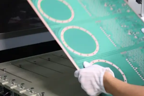
The most extreme example I’ve seen was an industrial-sensor company that skipped prototype validation and went straight to mass production, only to have connectors come loose across the entire batch during high-low temperature testing. In the end, they not only paid a breach-of-contract penalty but also had to reopen the mold for production.
Actually, good prototyping is like assembling building blocks — you need to check whether each individual piece is solid before confidently stacking them into a complete structure. A drone project I recently helped a friend with was a textbook example — through five rounds of prototype iteration, they improved antenna performance by 40%, something that would have been completely impossible to achieve once on the production line.
Some people always feel it’s too much trouble to have multiple manufacturers build prototypes, but it’s exactly that kind of comparison that reveals process gaps. Last week, comparing impedance-control performance between two factories, the exact same design file produced signal-integrity results differing by 15% — a difference that directly determines whether a high-speed interface can work reliably.
At the end of the day, PCB sampling isn’t a simple trial-and-error process — it’s what gives the design team room to breathe. Those seemingly repetitive validation steps often catch the most fatal problem before production begins. After all, nobody wants to see a warehouse full of unshippable products, right?
I’ve always found making PCB prototypes a genuinely interesting exercise — it’s like sketching a draft before assembling building blocks, just to see how it looks.
I remember once trying subtractive manufacturing for a small gadget and running into trouble — because I hadn’t fully considered how material thickness would affect signal transmission, the first attempt came out completely unusable! That’s when I understood why everyone emphasizes spending plenty of time on thorough, comprehensive testing at the early stage — after all, nobody wants to discover a problem only at the very end, right?
So now, before starting any new project, I always remind myself: don’t rush for speed at the expense of quality control — better to go a bit slower and make sure every step is done right.
Making PCB Prototypes reminds me of the first time I learned to ride a bike. At first, I always assumed finding a decent-enough manufacturer would settle things — it turns out that’s really not how it works. The prototype stage is like laying a product’s foundation — if the foundation is crooked, everything downstream has to be torn down and redone. I’ve seen too many teams try to save money and time on prototyping, only to have problems sprout up like weeds after rain once mass production begins.
A friend in smart-home products got burned exactly this way last year. The manufacturer they found made a four-layer board at the thickness of a double-sided board, and once powered on, signal interference was so bad it sounded like radio static. This kind of problem would have been easy to catch at the prototype stage, but rushing to meet a deadline, they skipped detailed inspection entirely. Re-sampling afterward delayed them two months, and team morale took a serious hit too.
Now, when communicating with partners, I always ask extra questions about process detail. For example, is surface finish immersion gold or hot-air solder leveling, is the board material’s Tg value high enough. These seemingly minor details often determine how the board performs in high-temperature, high-humidity environments. Sometimes a manufacturer gets impatient with too many questions, but compared to the cost of downstream rework, I’d rather be a demanding customer upfront.
A genuinely reliable manufacturer attaches a detailed test report when delivering a prototype. Inside the six-layer-board package I received last week was a yellowed slip of paper with handwritten impedance-measurement values for every via. That kind of old-school but conscientious attitude actually puts me at ease. After all, what we need isn’t the fastest or cheapest service — it’s a partner who can walk alongside the product from drawing to physical reality.
Recently, trying out a new manufacturer, I noticed something interesting. They proactively suggested enlarging a certain IC’s thermal pad area by 15%, even though it makes routing somewhat more troublesome. This kind of experience-based small improvement is often far more substantial than a price war. After all, when your product needs to work in a desert or polar environment, every extra dollar spent on the prototype is really insurance for reliability.
While recently working on an IoT-device project, I gained a new perspective on finding a PCB manufacturer. I used to think choosing a manufacturer was as simple as comparing price and lead time — now I’ve found there’s genuinely a lot more nuance to it. Especially when you need to sample, different manufacturers’ handling styles can directly affect project progress.
Once, I urgently needed a few prototype boards for testing and found a manufacturer claiming 24-hour shipping. The boards did arrive on time.
Every time I start a new project, I ask myself one question — what kind of PCB manufacturer do we actually need? This isn’t as simple as finding somewhere that can produce boards.
I’ve seen too many teams focus entirely on technical parameters while overlooking the actual collaboration experience. Those dense specification sheets do matter, but what genuinely determines a project’s success or failure is often the invisible stuff.
I remember a project last year where we found a manufacturer claiming to handle high-precision PCB Prototypes, and the first batch of boards ran into problems — not because their technical capability was lacking, but because communication was such a hassle. Every revision required back-and-forth emails, and even a simple question would drag on for days.
A good manufacturer should be like your partner, understanding your design intent rather than mechanically executing processing instructions. They’ll offer constructive suggestions right at the DFM stage, helping you avoid common pitfalls — that kind of forward-thinking advice is worth far more than fixing things after the fact.
Delivery time is another critical factor. I especially value manufacturers who can clearly commit to a timeframe — not necessarily the fastest, but with certainty. Compared to those who always say “as soon as possible,” I’d rather choose someone who gives a firm date, even if it means waiting two extra days — at least I can plan my downstream work accordingly.
Once, we ran into an urgent project needing fast iteration. That long-term manufacturing partner not only completed the PCB Prototypes ahead of schedule but also proactively offered testing suggestions. That kind of service beyond expectations made me realize choosing the right manufacturer significantly lowers project risk.
Now I pay much more attention to a manufacturer’s overall service capability, not just their technical specs. After all, making the board is only the first step — the follow-up support matters just as much.
I think a lot of people oversimplify PCB Prototypes. They think it’s just building a sample to see if it powers on — that’s really not how it works at all.
I’ve seen too many people, rushing for time, casually find a cheap manufacturer for sampling, only to hit revision after revision until they nearly break down. A friend who used to work on smart-home products rushed out the first version without even testing basic signal integrity, and once it hit mass production, severe interference showed up, requiring the entire batch to be reworked. That lesson hit deep.
The genuinely reliable approach is treating every prototype as a complete product validation. You need to check not just whether function is correct, but also whether the production process can keep up. For example, is trace width thin enough, will pads be too small — details ignored at the sampling stage become disasters at mass production.
Some manufacturers today have started using 3D printing to make circuit boards — a genuinely interesting development. Even though the technology isn’t mature yet, it does open up more possibility for design. That said, I think the key is still never skimping on the testing stage.
My own habit is to always leave enough testing time with every sampling run. Sometimes I even deliberately run extreme-environment tests — for example, performance under high-temperature, high-humidity conditions. It costs a few extra days, but it’s still better than problems surfacing later.
A recent project turned out exactly this way — it wasn’t until the third version that things finally stabilized. The first two versions technically worked but kept showing all kinds of small glitches under harsh conditions. Only after repeated debugging did we find that a component’s temperature rating wasn’t sufficient.
So, as anyone in electronics-product development knows: whatever corners you cut at the prototype stage, you’ll pay back double later. Rather than rushing frantically to catch up on schedule, it’s better to steadily and thoroughly validate every step.
I’ve seen too many teams treat PCB sampling as a simple procurement step. They think all it takes is sending out the Gerber files and waiting for the boards to arrive. This kind of thinking actually delays things quite a bit.
What genuinely matters is the interactive process between you and the manufacturer. A good partner proactively discusses design details with you — is trace-width spacing reasonable, will pad size affect soldering yield. They don’t just process to the drawing — they give you feedback grounded in engineering thinking.
I remember a project where the original prototype version kept having problems in the high-frequency section. Checking it ourselves repeatedly found no obvious error. It was later the manufacturer’s technical staff who suggested adjusting the grounding method, and performance immediately stabilized — proof that their experience filled in our blind spot.
When choosing a manufacturer, don’t just look at quote and lead time — the key is whether they can understand your design intent. Some manufacturers are cheap but genuinely painful to communicate with, having to explain requirements from scratch every single time, actually slowing down progress. Finding a partner who can speak your language raises efficiency enormously.
Many manufacturers today offer online ordering and progress tracking, which genuinely helps with fast iteration. You can see in real time which process stage the board is at, and adjust your plan promptly if there’s a delay. That kind of transparent workflow makes the entire development process far more controllable.
Quality stability can’t be overlooked either. Sometimes, rushing to save time, you choose an unfamiliar manufacturer, only to find impedance wasn’t controlled properly or the surface finish has a problem once the boards come back — forcing a redo, a genuine waste. Once you build a long-term partnership, the manufacturer understands your quality requirements better, reducing unexpected surprises.
At the end of the day, finding a PCB manufacturer isn’t a one-time transaction — it’s finding a reliable partner for your product’s entire lifecycle. Their technical support helps you avoid detours, and the transition from prototype to mass production also goes far more smoothly — a far more meaningful metric than simply comparing price.
While recently tidying up my studio, I dug up the very first PCB prototype board I made years ago, and looking at those crooked traces, I couldn’t help but laugh. Back then, I always assumed a multilayer board was something high-end — now I realize what genuinely tests skill is refining a simple design to perfection.
A friend in smart-home products complained to me last week that the four-layer board they paid a fortune to have prototyped by a manufacturer still didn’t get impedance matching right. Actually, a lot of engineers easily fall into the trap of chasing layer count. Once, taking over a drone project, the client insisted on an eight-layer-board design, and it later turned out six layers was fully sufficient, saving 30% of the cost.
Genuinely good design isn’t about how many layers you stack — it’s about how sensibly you allocate resources at each layer. It’s like building with blocks — you need to place critical signals in the safest position.
I remember once helping a student team revise their competition entry — their double-sided board layout was so chaotic they hadn’t even left space for thermal-dissipation holes. I walked them through replanning component placement, isolating the power circuitry separately, and ultimately achieved better performance at the same cost. This kind of good habit, formed right at the prototype stage, matters far more than fixing things later.
Now, when I see a design that treats a six-layer board as the default standard, I remember myself when I first started, always assuming complexity meant sophistication. In reality, the most elegant industrial-control board I’ve ever seen achieved perfect compatibility between gigabit Ethernet and motor driving using just four layers — the key was cleanly separating analog and digital sections like slicing a cake.
Every time I review a design now, I prefer looking at how well an engineer uses blank space. Boards crammed with components squeezed into every gap are actually more prone to problems — leaving white space is real technical confidence.
Making PCB prototypes is actually genuinely interesting. I’ve seen no shortage of people chase speed from the very start, eager to place an order today and get the board back tomorrow to test. But honestly, fast doesn’t necessarily mean good.
I remember once helping a friend look at a project whose board design was especially complex — using many layers of stack-up structure and involving a combination of different materials. Rushing to meet a deadline, they chose a supplier claiming three-day delivery, and once the boards arrived, the lamination clearly hadn’t been handled well — bubbles were visible between the board materials, and some areas even showed delamination. It all had to be redone, which actually delayed things even more.
I think what matters most when making a PCB prototype is understanding exactly what your design needs, rather than blindly chasing speed. This is especially true when using newer processes like additive manufacturing — you need to leave enough time in the process to fine-tune parameters, because while this technology can produce genuinely fine circuits, it demands extremely tight process control, and even a slight deviation can affect the entire board’s performance.
Another time, I tried making a high-frequency signal board myself, thinking that with few layers it shouldn’t be a big deal, so I chose a fast-prototyping service. Testing the board once it came back, signal integrity was a complete mess. Careful inspection afterward revealed impedance control hadn’t been handled properly, with dielectric-constant fluctuation causing severe signal attenuation. From that point on, I understood that for certain specific applications, you genuinely can’t rush.
Of course, this doesn’t mean rapid prototyping is unusable in every scenario. If your design is relatively simple — an ordinary double-sided board or four-layer board without strict impedance requirements — fast service genuinely saves a lot of time. But once high-density interconnect or special materials are involved, you need to be far more cautious.
My current approach is to assess the design’s complexity every time before making a new board. If I feel it might exceed the scope of a standard process, I communicate with the manufacturer ahead of time to see whether they have relevant experience or can offer process support. It might cost a few extra days, but at least it guarantees the board you get back is reliable.
After all, the whole point of prototyping is to validate the design. If inaccurate test results come from a problem in the manufacturing process itself, then the entire purpose of prototyping is defeated — don’t you agree?
I’ve always felt making a PCB is a lot like building with blocks — you need to first check whether the pieces in hand can actually form the shape you want. A lot of people jump straight into wanting mass production — that kind of impatience is dangerous. The worst case I’ve seen was a team that skipped prototype validation entirely, and the first batch of boards came back with the power module conflicting with the signal lines — the entire shipment had to be scrapped.
Actually, the fun of building electronics products is in the repeated tinkering. Once, helping a friend debug an audio board, the frequency-response curve looked beautiful in software simulation, but once actually soldered, we found the decoupling capacitors around the op-amp were placed too far away. This kind of problem is simply invisible without hands-on testing — you have to listen to the noise coming out of the speaker to understand what “the gap between the ideal and reality” really means.
Some younger engineers today rely especially heavily on simulation-software data, which is of course convenient, but never forget the importance of physical validation. It’s like cooking — you can’t just look at the recipe; you have to taste the seasoning yourself. I’ve made a habit of taking the board through different environments at the engineering-sample stage — testing heat dissipation in a hot workshop, testing signal stability in a location with heavy electromagnetic interference. Sometimes I’ll even deliberately push voltage to the critical threshold to see exactly when the board fails.
On the cost of PCB Prototypes, I think spending a few extra thousand dollars upfront on two or three iterations is far more cost-effective than a product recall later. I remember once, during a revision, discovering we’d chosen the wrong connector model — this kind of small detail is invisible on the drawing and only surfaces once you actually assemble the physical object.
What left the deepest impression on me was a smart-home project last year. The initial version, chasing thinness, packed the routing too densely, and mass-production yield never climbed. We later built a thicker prototype and spent two months testing before finally solving the problem.
At the end of the day, electronics-product development is a continuous process of trial-and-error. Those seemingly redundant validation steps are actually paving the way for the future. Even now, every time I see a new board’s power light turn on, I still feel that same excitement as the first time — that’s probably the romance of being an engineer.
When it comes to making PCB prototypes, I think a lot of people easily fall into a trap — always looking for the “perfect” service provider while overlooking the working style that genuinely suits them.
I’ve seen quite a few teams spend enormous amounts of time comparing parameters between different suppliers, actually delaying real development progress. In reality, the value of a PCB prototype lies in quickly validating an idea, not chasing flawless production quality.
I remember once, our team urgently needed to test a new design, and we went straight to a small local factory claiming 24-hour turnaround. Their online platform looked as crude as something built a decade ago, but they won out on direct communication. I sent the design file at ten at night, and the first batch of bare boards was ready by the next morning. The iteration advantage that speed brings is worth far more than waiting an extra week for so-called “perfect craftsmanship.”
Many companies today love bragging about their 3D-printing capability being able to integrate electronic and mechanical parts, but I personally hold a reserved view on that. Unless your product has special structural requirements, a step-by-step approach is often more efficient — focus first on stabilizing the circuit through debugging, then worry about enclosure fit.
Assembly is even more like that. Some teams put blind faith in a fully automated process and forget how important manual inspection is. Once, we received a batch of boards that looked flawless on the surface, only to find a critical component had been placed backward — even the smartest system has a hard time catching that kind of problem in time.
At the end of the day, the core of prototyping is trial-and-error efficiency. Rather than agonizing over a supplier’s ranking or technical buzzwords, it’s better to build a stable partnership. Finding a partner who understands your design intent and can give you fast feedback on problems beats everything else.
I’ve increasingly come to feel that good prototyping should be as natural as chatting with an old friend. You don’t need to explain too much background — they grasp the key point right away; when a problem comes up, a single phone call clears it up. That kind of efficiency gain from mutual understanding is something no advanced technology platform can replace.
Of course, this doesn’t mean rejecting new technology either. For example, we now first build a rough structural mockup with 3D printing, fit the PCB inside to check the layout, and only then finalize it. But that kind of supporting experimentation is a different matter entirely from blindly chasing technology integration.
Finally, I want to say — don’t let flashy service terms dazzle you. What genuinely matters is always: can your design quickly become a testable physical object? Can problems be adjusted promptly when they arise? Whether the platform looks cool or the technology is cutting-edge is secondary.
After all, we’re doing product development here, not attending a tech expo!
I’ve seen too many teams stumble at the PCB prototyping stage. They always assume finding a manufacturer who can prototype quickly is enough, only to discover once they receive it that even basic function doesn’t run. Actually, choosing a manufacturer is far more complicated than most people think.
Sometimes your parameters look perfectly compliant on paper, but actual soldering still runs into problems. That’s when, if the manufacturer can give you reliable engineering feedback, it often saves several rounds of revision time. I once worked with a particularly meticulous manufacturer whose engineers would inspect every single via with a magnifying glass — delivery was two days slower, but downstream debugging efficiency was actually much higher.
Many manufacturers today boast about how advanced their equipment is, but what genuinely matters is whether they understand your design intent. A good manufacturer should be able to point out potential risk in your design, rather than waiting until the board fails to start arguing over responsibility. I remember once we had a high-frequency circuit requiring special handling, and the other side’s technical director spent half an hour on a video call explaining impedance-matching key points — that kind of support is worth far more than any certification.
The validation stage can’t be treated carelessly either. Some small factories skip necessary inspection steps to save cost, only to discover appallingly low yield once mass production begins. I’ve made a habit, on any first collaboration, of placing a small trial order first, focusing on checking whether their quality-traceability system is sound. After all, every problem at the prototype stage could affect downstream mass production.
At the end of the day, finding a manufacturer is like finding a partner — looking at price and equipment alone isn’t enough. What matters most is whether they’re willing to spend time understanding your needs, and whether they can offer constructive input at the technical level. After all, what we need isn’t simple processing service — it’s a partner who can solve problems together with us.
I’ve seen quite a few people whose understanding of PCB Prototypes still stays at a fairly basic level. They think making a prototype just means connecting the circuit and making sure it powers on. This kind of thinking actually overlooks a lot of key factors.
I remember once helping a friend check a board that kept having problems. On the surface, all the traces were connected, but it just wouldn’t run stably in actual operation. It later turned out a conductive path in a certain area had been designed too casually, causing signal interference with each other. That incident made me realize a prototype’s value isn’t just about achieving function — it’s even more about exposing hidden problems in the design.
Many people today, the moment innovation comes up, think of using the newest technology — for example, printing the entire circuit board directly. That approach genuinely is convenient in certain specific scenarios, but I’ve found it often can’t solve complex problems. Especially when circuit density is high, traditional manufacturing methods are actually more reliable in guaranteeing reliability.
I prefer building several different-scheme prototypes early on and running comparative testing. Sometimes a seemingly simple change produces unexpectedly good results — for example, just adjusting a component’s placement can significantly improve thermal dissipation.
Some tools today genuinely make the manufacturing process simpler, but that doesn’t mean we can skip necessary validation steps. After all, no matter how advanced the printing technology, it can’t replace the importance of actual testing.
Every project has its own unique needs — no single method is universally applicable. We need to make the right choice based on the specific situation — that’s the real meaning of doing prototyping well.
After years of making PCB Prototypes, I’ve developed one particularly strong realization — sometimes the more expensive option is actually the more cost-effective one. I remember a medical-device company’s first time working with us, insisting on procuring all their own components — the project dragged on for two months and was still missing a critical chip. Switching to our in-stock components, we shipped the board in three days.
Many people think outsourcing component procurement adds cost, overlooking a key point — time is money too. Having your engineer spend two weeks shopping around for a supplier isn’t as good as letting them debug two more circuit revisions instead.
I’ve seen too many clients agonize excessively over BOM cost at the prototype stage — especially startup teams, always wanting to squeeze it down to the absolute minimum, when what genuinely deserves attention is iteration speed. Last week, a smart-home client had originally chosen a cheap sensor with a long lead time; I suggested switching to an in-stock model three dollars more expensive, ready for placement the next day — as a result, he collected five sets of samples within three days, validating the thermal-dissipation issue ahead of schedule.
Component-market volatility is severe these days, and self-stocking carries real risk. Once, helping a robotics team handle an emergency substitution, their designated main-control chip suddenly went out of production — fortunately, our warehouse had a functionally similar alternative, and a slight circuit modification kept the project moving.
Actually, a good prototype manufacturer is more like a partner who can anticipate risk. Last year, building a controller for a new-energy vehicle, we found the connector the client chose had insufficient temperature rating — even though it was still within the quoted scope, we proactively suggested switching to a pricier industrial-grade version. They ended up genuinely avoiding a disaster during high-temperature testing later.
Sometimes, when a client shows up with a densely packed component list, I’ll first ask which items are genuine performance requirements and which are just habitual choices. Once, we helped a drone team consolidate twenty resistors into a single array package, shrinking board area by 15% directly.
At the end of the day, what a prototype competes on isn’t perfection — it’s fast validation. The market moves so quickly these days that by the time you’ve haggled every single component down to rock-bottom price, a competitor might already be three generations ahead.
Every time I see one of those articles making PCB manufacturing sound almost mythical, I can’t help but laugh. Cost advantage, technology leadership, global footprint — these big buzzwords sound impressive, but anyone who’s actually run a few projects knows finding the right PCB manufacturer is nothing like that.
When I first got into hardware design, I made the same mistake too, assuming the lowest quote was the right choice. The first batch of boards came back with pads off from the drawing by half a millimeter, and impedance control was a complete fantasy. I later understood that a good PCB manufacturer needs to understand your design intent the way an experienced doctor reads a pulse. They need to know where precision genuinely must be nailed down, and where there’s room for flexibility.
Now, when looking for a supplier, I pay especially close attention to their prototyping process. Some factories treat a sample like mass production, practically issuing a full inspection report for every single step. But actually, for a board at the validation stage, fast trial-and-error matters more than flawless perfection. Once, on an RF project, the partner factory’s manager called me directly and asked: “Should we do half-side impedance matching first on the second version? That’d save two days.” That kind of insider-level suggestion was worth far more than an 18% price cut.
Speaking of domestic alternatives, that’s genuinely interesting too. Plenty of domestic manufacturers today can genuinely produce high-performance materials, but the problem often shows up in detail handling. For example, with the same high-frequency board material, some factories consistently leave tiny bubbles at the board edge during lamination — it doesn’t affect performance, but it plants a landmine for downstream assembly. So now, when I look at a supplier’s sample, I specifically check those inconspicuous spots.
I’ve recently noticed something genuinely interesting: some small-batch PCB manufacturers are actually better suited for innovative projects than large factories. Their equipment might not be as advanced, but their engineers are willing to spend half an hour studying your stack-up design. Compared to grand ambitions of building a factory in Southeast Asia, that kind of focus puts me far more at ease.
At the end of the day, choosing a supplier is like finding a partner — hardware specs alone are useless. What matters is whether they understand your design philosophy, whether they’re willing to stay up late with you at critical moments to revise a plan. After all, no process standard, however good, beats a manufacturing partner who genuinely knows the business — a distinction that matters just as much whether you’re sourcing from a general multilayer pcb supplier or a specialized high Frequency PCB manufacturer.
Do you think a rain sensor is just a simple circuit board?
Sunroof control PCB design is easy to get wrong when teams are
As a veteran hardware engineer, I’ve found that a lot of people
- Pienten ja keskisuurten erien tuotannon asiantuntija
- Korkean tarkkuuden piirilevyjen valmistus ja automatisoitu kokoonpano
- Luotettava kumppani OEM/ODM elektroniikkaprojekteihin
Aukioloajat: (ma-la) klo 9:00-18:30.
Get quote, solution or any question, Andre always here to help