

Why the Best PCB Supply Chains Are Built Like Relationships, Not Transactions: Lessons for Satellite Communication PCB Programs
What actually makes a long-term PCB supply chain partnership work — shared
Why We Nearly Blew Production Because We Ignored the PCB Until Too Late
Not long ago, a project nearly went off the rails — building a communication baseboard for a new vehicle’s domain controller. At the time, we poured all our effort into chip selection and software architecture, and it wasn’t until two months before mass production that we found ourselves stuck on the most basic link of all: the PCB. Looking back now, a lot of people’s understanding of this area is actually fairly one-sided — always thinking that finding a multilayer board supplier and handing them a Gerber file is the end of the job.
In reality, an Automotive Communication Module PCB is a completely different animal from an ordinary digital circuit board. The equipment inside a car doesn’t just sit on a desk pushing data — it has to withstand cold starts at minus forty degrees, endure sustained high temperature near the engine bay, and guarantee that over ten years, board delamination or CAF failure won’t take down the entire CAN bus. Several of the multilayer board suppliers we worked with initially assured us confidently there’d be no problem, but the moment thermal-cycling testing began, via fractures and snapped copper traces were everywhere.
We later found the problem was that they had no concept at all of thermal-stress accumulation in an automotive environment. An ordinary consumer-electronics PCB’s lifespan is at most three to five years — once an automotive communication module is installed, it’s essentially expected to last as long as the vehicle body itself. If it fails midway, the labor cost of replacing it can exceed the cost of the part itself. So when we later screened suppliers, we didn’t look at the shiny samples on their trade-show booth at all — we went directly to the production line to look at their lamination process and inner-layer inspection capability, especially their experience with thick-copper mixed lamination and multi-order HDI boards.
There’s another easily overlooked point: how much a board material’s dielectric constant changes with temperature. Many automakers today are pushing gigabit or even ten-gigabit automotive Ethernet as the backbone network — the moment differential-pair impedance control drifts even slightly, the eye diagram closes outright. Some multilayer board suppliers’ recommended high-Tg materials look great at room temperature, but above 85°C, the DK value drifts badly, and signal integrity simply can’t be guaranteed. We tested several domestic board materials ourselves and found two companies whose hydrocarbon resin systems were actually quite solid — high-temperature stability no worse than Rogers, at roughly one-third the price — though their production capacity often couldn’t keep up with demand, which is genuinely a headache in the supply chain.
On the topic of vehicle electrical/electronic architecture, I actually think the industry has become a bit too enamored with central-compute platforms right now. Stuffing every ECU’s function into one box is theoretically clean, but the moment the main control board inside that box fails, the entire vehicle goes dead — the functional-safety risk is too high. I lean more toward a hybrid zonal-plus-lightweight-central approach — distributing high-real-time-requirement communication processing across several zonal gateways, keeping each region’s PCB scale from getting too large, making thermal dissipation easier and fault isolation possible, while also lightening the load on the main control board. This approach actually places higher demands on multilayer PCB design, because you need to cram isolated power for multiple buses into a limited area — including CAN FD termination matching and Ethernet common-mode filtering — a pile of details that, handled poorly, will fail an EMC test outright.
Last year, one of our design revisions failed exactly because we overlooked the ground-loop routing of the LIN transceiver, causing the entire communication module to repeatedly reset during BCI injection testing. It took two weeks of troubleshooting to trace it back to a misplaced split line on layer two of a four-layer board — after revision, it passed immediately. This lesson was deep enough that now, at every design review, I insist the layout engineer draw out the return paths for those critical loops, whether they find it tedious or not.
Ultimately, an Automotive Communication Module PCB tests not a single technical point, but a team’s reverence for whole-system reliability — and whether the multilayer board supplier genuinely understands what “automotive-grade” means, rather than simply printing AEC-Q100 on the spec sheet and calling it done.
Why Chip Specs Alone Never Tell You Whether the Board Will Survive
After many years in automotive electronics, I increasingly feel that choosing a communication module was never something you could settle just by sitting down and comparing chip-datasheet parameters. Very often we get overly absorbed in how many ports a switch chip supports, or how many fewer milliwatts the PHY draws, while overlooking the more fundamental thing: the board itself. What you’re holding is an Automotive Communication Module PCB — it’s not a simple substrate. It has to carry away tens of watts of heat while guaranteeing signal integrity across an environment from minus forty to over a hundred degrees. I’ve seen too many teams obsess over chip compute power during selection, only to discover at the mass-production stage that the PCB stack-up design was unreasonable, high-speed differential-pair impedance drifted badly, and the module’s packet-loss rate simply couldn’t be brought down.
You first need to clearly determine exactly where in the vehicle this board will sit. Sitting quietly inside a cockpit domain controller, or stuffed near the engine bay, getting shaken numb all day long? This determines what requirements you should raise when finding a multilayer PCB supplier. Some suppliers specialize in consumer-electronics boards — beautiful process, low price — but the moment you mention automotive-grade high-Tg material, or lamination-uniformity control down to the micron level, they start hedging. I got burned once, using a factory with no automotive-grade experience — the result was the board delaminated outright during thermal-shock testing, copper-foil peel strength nowhere near adequate. We later switched to a factory specializing in automotive boards — from the very start they recommended a mixed lamination structure, separating the power layer from the high-speed signal layer, and specifically adjusted the prepreg type to reduce CAF (conductive anodic filament) risk. None of these details are visible just from reading a chip datasheet.
On the topic of module-level comparison — many people think a zonal controller is simply an upgraded traditional gateway, just integrating more functions. But once you actually build it, hardware complexity rises exponentially. What used to be handled by a four-layer board with a simple MCU as the main controller for a CAN gateway now needs to support Ethernet, needs to support TSN, and needs to reserve a PCIe interface for a 4G/5G module — that’s no longer something a four-layer board can handle. I especially dislike the idea that “swapping in a bigger chip solves it.” Change the chip, and the entire power tree has to be redone — you need to calculate voltage drop, consider Vcc ripple’s effect on the PLL, or TSN’s clock-synchronization precision simply won’t reach spec. These all need to be compared at the system level right at the selection stage — not by looking at chip specs alone.
Also, don’t blindly worship the central-compute-unit communication baseboard the moment you start. This kind of architecture does look clean, but concentrating all communication onto one board also concentrates the risk. Once that board fails from a local short circuit or an EMC issue, the entire vehicle can go dead on the spot. Moreover, this kind of oversized PCB places extremely high demands on a supplier’s process capability — for example, how to guarantee overall board thickness tolerance during lamination, how to avoid warpage causing BGA cold joints. Not every multilayer PCB supplier can take this on. I actually think, on some projects, keeping an independent communication-gateway module, or making it a standardized daughter card, is smarter than piling everything together — both for iteration flexibility and fault isolation.
Ultimately, selection isn’t a contest of who knows more — it’s a contest of who knows how to make trade-offs. I often remind myself: don’t get led astray by a supplier’s demo board — it uses the most ideal stack-up and materials, a world away from mass production. You need to think through the worst case first: how badly will the signal eye diagram close under high temperature, could common-mode noise couple into the RF front end through the power plane, could via impedance drift as the board ages. Once you’ve thought this through, and go back to look at those beautiful curves in the chip datasheet, you’ll have a much clearer scale in your mind.
Why the Gateway Role Has Become a Language-Barrier Translator
Anyone in automotive electronics knows that small, unremarkable-looking communication-module PCB actually determines whether data inside the car can flow smoothly. I recently talked with an engineer at a multilayer PCB supplier, and he complained that automakers’ requirements have become increasingly outlandish — one board needs to run high-speed Ethernet while also being compatible with the old LIN bus, forcing the stack-up from four layers up to eight, with impedance control precise to two decimal places. This actually reflects a very real problem: during architecture design, everyone wants to go straight to all-Ethernet in one step, only to find, once it lands, that things like window controls and seat adjustment still need LIN to keep cost down.
The gateway’s role becomes especially awkward as a result. In the ideal architecture, it should be a lightweight data router, but the reality is it has to simultaneously translate CAN FD, LIN, and even some proprietary protocols — turning it into a translator dealing with languages it can barely understand. The most outlandish project I’ve seen had a gateway MCU running at over 80 percent load long-term, just from handling the trivial signals sent up by several hundred LIN nodes. I eventually recommended they stop fighting it out at the gateway layer, and push some edge compute down to the zonal controllers, letting the gateway handle only policy-based data forwarding. This approach was actually borrowed from multilayer board design thinking — separating the signal layer from the power layer, isolating what needs isolating, not letting interference bleed across the whole system.
On the topic of multilayer boards, finding the right supplier is critical. Many factories tout their ability to build “automotive grade” boards, but the moment you actually hand over the Gerber file, they can’t even properly calculate differential-pair length matching. I got burned once — a batch of boards, due to layer-to-layer dielectric thickness deviation, caused the Ethernet eye diagram to close, and the entire batch had to be scrapped. We later switched to a multilayer PCB supplier specializing in automotive communication modules — they even select copper-foil roughness based on signal frequency, and that’s what finally solved the problem. So now, when I look at a board factory, I don’t look at how many certifications they have — I look at whether their engineers can clearly explain why the surface layer’s LIN signal traces should use mesh copper rather than solid copper.
Actually, automotive electronics is a fairly interesting field — technology evolves with a lot of fanfare, but once it lands on the PCB, it’s all a micron-level negotiation. Anyone loudly proclaiming the complete elimination of CAN and LIN has probably never actually laid out a board themselves.
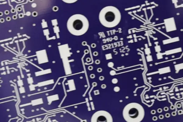
Why an 8-Layer Board With Beautiful Chip Specs Still Failed the Eye Diagram
Over the past couple of years, I’ve worked on quite a few domain-controller and smart-cockpit projects, and noticed a particularly interesting phenomenon — the moment automotive communication modules come up, everyone’s attention locks onto the chip, as if selecting a certain Ethernet-capable SoC settles everything. But once you actually get the board running, the problem is often in the PCB itself — especially the Automotive Communication Module PCB.
Let me give an example. On a previous project, we tripped up on an automotive Ethernet switch chip. The chip’s own specs looked beautiful — supporting multiple 2.5G channels, power consumption reasonably restrained. But when we handed the schematic to a multilayer PCB supplier for prototyping, they built an eight-layer board using a conventional stack-up plan. When it came back and we tested it, the high-speed differential pairs’ eye diagram wouldn’t open at all — signal integrity was a mess. We later found a supplier specializing in automotive radar boards — they understood far more than we did about layer-to-layer dielectric thickness and glass-fiber-cloth selection, and directly recommended a low-loss M4 material, giving explicit control ranges for copper-foil roughness on adjacent layers. After the revision, using the same chip, signal quality was completely different.
This taught me a lesson: in automotive Ethernet, the PCB’s position is far higher than you’d imagine. You can’t just find any factory capable of processing multilayer boards to handle it. The higher a chip’s integration level, the more sensitive the PCB’s trace density, power integrity, and thermal-dissipation copper design become. Especially under today’s domain-control architecture, one board needs to cram in an MCU, switch chip, PHY, plus a pile of eFuse and PoDL power circuits — heat sources clustered together, and no amount of poring over the chip datasheet solves anything. You need to deeply engage with the PCB supplier, letting them understand your stack-up intent, even requiring them to provide impedance-test coupon reports, rather than trusting their verbal promise that they can “default to 100-ohm differential.”
I later developed a habit — pulling a multilayer PCB supplier’s process-capability data into the project at the proposal stage, rather than waiting until the schematic is finished. For example, I’ll have them first provide the current board material’s dielectric constant and loss tangent at 1GHz and 2.5GHz, and then I use these parameters for simulation, rather than the ideal model given by the chip vendor. Only this way does the result match up with actual prototyping. Many friends think this is redundant, but only someone who’s been burned understands: once an automotive communication module’s PCB causes Ethernet-link packet loss because of a signal-integrity issue, debugging the upper protocol stack alongside it becomes a nightmare — you can’t even tell whether it’s a chip-driver problem or a physical-link problem.
Overall, I think the industry’s current worship of chips has gone a bit too far, leaving the PCB — this foundational discipline — neglected instead. Five years ago, in the era of low-speed CAN/LIN buses, PCBs really could be drawn casually. But now that Ethernet is becoming widespread, especially when carrying raw video streams and radar data, a good Automotive Communication Module PCB and a reliable supplier are the real key to keeping your link genuinely stable.
Why the Communication Module Should Be Treated as Flowing Glue, Not a Fixed Block
I recently helped a domain-controller team review their board — they’d been stuck on the communication module’s layout for a full two months. The problem was very typical — they were too eager to treat the Automotive Communication Module PCB as an independent small board. This approach might have worked five years ago, but if you’re still piling on materials in the traditional standalone-gateway form today, the resulting bandwidth will absolutely be insufficient, and thermal dissipation will be a mess. Many people haven’t realized that automotive communication modules should no longer be viewed as a “module” — they’re more like a kind of glue that flows with compute demand, needing to seep in wherever high bandwidth and low latency is needed.
Among the multilayer PCB suppliers I’ve worked with, genuinely few truly understand this shift. Most factories still hand you a proposal based on consumer-electronics stack-up experience — jumping straight to recommending 8 or 10 layers, and when you ask why, they say there are a lot of high-speed signals. But the difficulty in an Automotive Communication Module PCB was never layer count — it’s how you control impedance consistency for PCIe or multiple SerDes groups within a total board-thickness limit of 2.0mm or even thicker, while also suppressing heat. If a multilayer board supplier hasn’t done automotive-grade high-current copper thickness and inner-layer copper balancing before, the signal shift caused by board warpage later on will make you question everything. I got burned by this — afterward, when selecting suppliers, I always first check whether they’ve done batch production of buried copper blocks or local mixed-lamination schemes — even at slightly higher cost, that’s better than the board blowing up.
Now let’s talk about form factor. Many people today shout about central-compute platforms integrating everything, as if the communication module will eventually disappear. I don’t think it’s that absolute. Compute is consolidating toward the center, but the physical wiring harness hasn’t disappeared — the vehicle body’s sensors and actuators are becoming increasingly distributed. You can’t run a thick, expensive gigabit Ethernet cable back to the central brain from behind every LiDAR. So the future form factor will be a kind of “distributed spine” — the central unit retains the strongest compute for fusion processing, but the zonal communication baseboards will miniaturize, even become a kind of flex PCB attached to the vehicle body frame. This kind of small Automotive Communication Module PCB isn’t sensitive to layer count, but has extremely demanding requirements for the stack-up material’s dielectric constant and loss factor, because you need to run hundred-megabit -T1 or 1-T1 signals in a palm-sized area, while also withstanding the cabin’s outside temperature-humidity cycling.
The relationship between bandwidth and compute is also often misunderstood. It seems like more compute should mean mindlessly piling on more bandwidth. Actually, in high-level autonomous driving, what genuinely consumes bandwidth isn’t compute itself — it’s moving raw sensor data. For example, an 8-megapixel camera running at 30fps, if uncompressed, can saturate a 1Gbps link on its own. But if you do preprocessing at the front end, using edge compute to extract feature points before transmitting, bandwidth demand drops by an order of magnitude immediately. So when designing a communication baseboard, you can’t just look at the SoC’s peak compute — you need to factor in the entire data flow’s compression strategy and sensor-fusion approach. I saw a project using Orin-level compute, where the communication baseboard only reserved a 100Mbps -T1 channel for radar, because they’d moved point-cloud processing to the zonal controller, and the center only received the object list — that’s clever, the board is easier to build, and cost is under control.
Many multilayer PCB suppliers now love pushing full-board blind/buried vias, which look advanced, but aren’t necessarily suitable for an automotive communication module. Blind/buried vias do improve routing density, but an automotive board’s lifespan is calculated at 15 years or longer — repeated thermal shock will crack the bottom of a blind via, a failure mode that would never surface in consumer electronics. I lean toward using through-holes as much as possible, then guaranteeing signal return paths through optimized stack-up design, and won’t easily go with blind/buried vias unless density genuinely can’t fit otherwise. This experience came from a supplier specializing in automotive radar boards — they’ve supplied millimeter-wave radar boards to Tier 1s for over a decade, using blind vias extremely sparingly, but with extremely well-controlled yield.
Why CAN FD Still Beats Ethernet for Most Sensor Aggregation Tasks
I’ve worked on quite a few domain-controller and zonal-gateway projects. Nowadays, everyone jumps straight to talking about automotive Ethernet, as if not using 100BASE-T1 makes you obsolete. But in actual operation, many scenarios don’t need that much bandwidth at all — forcing Ethernet on actually makes the entire hardware design especially awkward. The most outlandish case I saw: a Tier 1, to aggregate data from several sensors on a vehicle, insisted on using Ethernet — the result was the board needed two extra layers, and just debugging the common-mode choke and ESD protection took nearly two months, and in the end the BOM cost was almost forty dollars higher than a CAN FD-based solution. What forty dollars means in a passenger car, I don’t need to elaborate.
So now I lean toward treating the Automotive Communication Module PCB as a cost-allocation game. The key isn’t chasing what’s new — it’s clearly understanding the real throughput needs of every communication port. CAN FD at 5Mbps is more than adequate for diagnostics and body control, and its fault-tolerance mechanism and maturity are something automotive Ethernet can’t catch up to in the short term. I even think the industry has put too much effort into the 802.1 family of standards — putting the cart before the horse. It’s not that TSN doesn’t matter — it’s that 802.1Qbv’s gate scheduling and 802.1Qav’s credit shaping are extremely painful to tune in real multi-hop mixed traffic. The moment software configuration gets complex, the probability of something going wrong is higher than with hardware, and many chips claim to support 802.1AS-Rev time sync, but actual testing shows end-to-end jitter still can’t be controlled, ultimately requiring software patches to compensate.
When selecting a chip, don’t just look at port count. The biggest pitfall I fell into was a switch chip claiming to support the full TSN feature set — only after buying it did I discover its 802.1CB frame replication and elimination function only works under specific port combinations, and once hardware MACsec is enabled, line rate directly drops by half. This kind of detail is never explicitly stated in the datasheet — you can only test it yourself on a bench. So I later just locked in two multilayer PCB suppliers, having them get involved early to help me evaluate how routing and vias affect 100-ohm differential impedance. Because once you go above 2.4Gbps multi-gigabit Ethernet, board layer count and material selection matter more than the chip itself. I stick with a supplier who can stably produce 4-layer mixed lamination with a Tg no lower than 175°C — even at a slightly higher price, that’s far better than PHY packets dropping frequently later due to impedance deviation, driving you to question everything while chasing the root cause.
In the automotive Ethernet race, I think what genuinely needs to be competed over isn’t the chip — it’s the PCB. However powerful a chip’s features, if it can’t fit into a board meeting cost requirements, it’s worth nothing.
Why Board Consistency Matters Ten Times More Than Beautiful Parameters for TSN
Talking about the PCB in automotive communication modules, my biggest takeaway over the past couple of years is that the old days of “find a multilayer board supplier, draw it per reference design, and call it done” are long gone. Now, the moment TSN is involved, every hardware decision is tightly bound to real-time performance — move one trace, and the entire clock-sync scheme could shift out of alignment. This isn’t a joke.
I handled a project where, selecting the supplier for the Automotive Communication Module PCB, we nearly stumbled on the multilayer board’s dielectric-constant tolerance. Many companies claimed they could do high-Tg, low-loss material, but very few could actually guarantee stability batch to batch. One claimed tolerance controlled at ±0.05, but actual measurement showed the dielectric constant could vary by 0.2 at different positions on the same board — for Ethernet signals above 125MHz, this closes the eye diagram outright. We later switched to a smaller multilayer PCB supplier — their equipment didn’t look as impressive, but their process discipline was extremely strict, correcting residual copper ratio after every layer’s lamination against actual impedance — the resulting board consistency was far better. This made me realize that at the hardware level for TSN, stability matters ten times more than beautiful parameters.
On the topic of real-time performance — many people think it’s just software timestamping and configuring gPTP, and that’s it. But the pitfalls on the hardware side run much deeper. Take the interface between the switch chip and the PHY — RGMII’s delay compensation — if the PCB design doesn’t enforce length matching, or the reference-plane split is unreasonable, nanosecond-level jitter gets amplified by TSN’s scheduling mechanism. I saw a case where, under full load, a zonal controller’s CAN message pass-through delay would occasionally spike to several hundred microseconds. Tracing it to the end, we found a differential pair on the PCB wasn’t ground-guarded, and was disturbed by switching noise from a nearby DC-DC converter, causing frequent MAC-layer retransmission — the application layer directly perceived “real-time” turning into “erratic.” So now, when I look at hardware, I always focus on board-level EMC and power integrity — that’s more effective than switching to any high-end SoC.
Hardware architecture choice is also closely tied to how TSN is implemented. Some chip vendors delegate traffic shaping and gate scheduling entirely to an on-chip hardware accelerator, with the CPU barely involved — in this case, the PCB’s stack-up design needs to prioritize guaranteeing a low-latency path between the chip and the external PHY, rather than blindly chasing layer count. Other schemes rely on software for scheduling, which places extreme demands on memory bandwidth and interrupt response — hardware then needs to make DRAM traces extremely short and give the real-time core independent power, preventing it from competing for current with other logic. Neither is absolutely better — it depends on what problem your TSN profile actually needs to solve. I actually think a multilayer PCB supplier who’s thoroughly grasped these hardware details is far more valuable than one who simply knows how to laminate a ten-layer board.
Why “Supports TSN” on a Datasheet Means Almost Nothing at Minus Forty Degrees
I’ve recently worked on several domain-controller projects in a row, and almost every requirement list included TSN support, as if not attaching this acronym makes something less advanced. But once you actually dig into hardware design, you’ll find this is far more complex than printing “supports TSN” on a datasheet. I’ve seen quite a few chips where the vendor talks up the 802.1AS timestamp unit endlessly, but the moment it’s on a board, synchronization precision across the full temperature range simply can’t stay stable — especially at the -40°C end, where the crystal’s own frequency drift combined with power-noise coupling can push master-slave clock offset straight up to several hundred nanoseconds — at which point all the gate scheduling becomes decorative. Ultimately, hardware-level time-awareness capability can’t be guaranteed by the chip alone — board-level routing, stack-up, even the process consistency of the multilayer PCB supplier you choose, all discount that seemingly perfect TSN spec.
The Automotive Communication Module PCB’s role in the whole chain is actually far heavier than most people imagine. Poorly controlled phase consistency in high-speed differential pairs causes PTP messages to develop asymmetric delay right at the physical layer — no amount of software calibration afterward can fix that. Once, to catch up on schedule, we switched to a lower-priced multilayer PCB supplier, and the resulting impedance fluctuation directly raised the automotive Ethernet packet-loss rate, triggering the frame-replication-and-elimination redundancy mechanism frequently — the entire system’s determinism actually got worse. This made me thoroughly understand: TSN isn’t something you achieve by buying a pile of 802.1Qbv-capable switch chips and soldering them onto a board — it tests your control over the entire chain, from chip selection, to clock-tree design, to PCB manufacturing tolerance.
Now, whenever I see a scheme touting TSN as a selling point while glossing over hardware details, I instinctively raise a question mark. Genuinely reliable coexistence of mixed critical traffic doesn’t rely on some feature of some chip — it relies on how much effort you’re willing to put into layout, and how much you’re willing to invest in real-environment test validation. Functional safety is the same — once ASIL decomposition is done, hardware metrics point directly to random hardware failure. If the multilayer PCB supplier’s process report can’t produce data on copper-thickness uniformity and layer-to-layer registration accuracy, however elegant your designed redundant link, it could still fail from a micro-short or an impedance jump. So perhaps more important than agonizing over whether a chip supports TSN is first finding a board factory that can build your carefully designed stack-up exactly as intended.
Why a Buried Via’s Z-Axis Fracture Defeated an ASIL-D Design
Working in this field for years, I increasingly feel that whether an Automotive Communication Module PCB can withstand the harsh environment inside a car often doesn’t hinge on those beautiful ASIL-level annotations on the drawing — it hinges on the invisible details inside the multilayer PCB supplier’s workshop. Everyone talks about “safety first,” but once it lands on the hardware, many people still stare at the diagnostic coverage rate on the chip datasheet, forgetting that once an internal-layer micro-short occurs even once under vibration and thermal shock, the entire communication link goes completely dead.
This isn’t scaremongering. I handled a domain-controller project where the ADAS signal ran on a 12-layer board, with ASIL-D decomposition done extremely rigorously — physically isolating high-level and low-level paths, even using different ground layers. But precisely because the multilayer PCB supplier’s lamination process wasn’t stably controlled, after a few hundred thermal cycles, Z-axis expansion directly tore apart the buried via responsible for the safety path. At the time, none of the diagnostic mechanisms had a chance to report an error — the MCU’s lockstep core couldn’t detect this kind of physical-layer failure at all, because it wasn’t a logic error — the circuit had physically broken. That’s when I realized that elegant decomposition at the hardware-architecture level is completely useless in the face of rough manufacturing. This kind of failure mode is extremely hidden — the buried via sits at an internal layer, invisible to visual inspection, only confirmable through X-ray or cross-section analysis, and conventional electrical testing often passes under static conditions, only surfacing under dynamic stress once the vehicle is on the road.
So now, when I select a multilayer PCB supplier, I don’t look at how many layers they can support, or what minimum trace width and spacing they can hit. What I care about is their control over glass-fiber-cloth weave pattern — for example, the fiber-bundle-gap difference between opened-weave and plain-weave cloth — at Ethernet transmission above 10Gbps, uneven weave pitch introduces picosecond-level delay deviation, directly worsening differential-pair phase consistency. Whether they run batch-to-batch consistency testing on DK’s temperature variation — I once saw a supplier switch resin formula without notification, causing dielectric constant to spike at -40°C, causing originally matched trace lengths to suddenly detune, causing radar-signal frame loss. And whether they run stress simulation for mixed lamination of thick-copper regions and signal regions — this simulation can predict uneven resin flow caused by copper-thickness difference during lamination, avoiding stress concentration at microvias from CTE mismatch during later reflow or thermal cycling, which could trigger fatigue cracks. These are the things that genuinely concern safety. A car has to run back and forth between the winter of Northeast China and the summer of Turpan — if the board’s dielectric constant drifts significantly, even a small impedance jump will prevent a high-speed signal’s eye diagram from opening, and the end-to-end protection mechanisms ASIL requires often trigger inexplicable fault codes at the exact instant the CRC can’t compute.
I even think that over-reliance on ASIL decomposition can sometimes cause people to overlook something more fundamental. However safely you draw the communication path, if the board’s own power integrity has a problem — say a transient current causes the reference plane to collapse — the CAN FD or Ethernet physical-layer waveform running on top will distort outright. Just like when electric power steering suddenly engages, a large current pulse excites wideband noise on the ground plane, coupling into an adjacent CAN bus — even with a common-mode choke at the physical layer, it’s hard to fully suppress this kind of board-level crosstalk. Software and diagnostic logic are completely powerless against this kind of thing. So now, when I look at a hardware design scheme, I spend a lot of time studying the Automotive Communication Module PCB’s stack-up and power distribution, checking whether the supplier genuinely has experience separating high-di/dt loops from sensitive analog front ends, rather than simply placing a few isolation components on the schematic and calling it done. Ultimately, the reliability of that board inside a car grows out of the lamination press’s parameters — it’s not filled in from an FMEA spreadsheet. For example, the temperature-rise rate and pressure uniformity during lamination directly determine resin fill rate and layer-to-layer bond strength — once these parameters deviate from the optimal window, however high your design redundancy, it won’t withstand long-term vibration testing.
Why the Same Chip Performed Differently Once the Layer Impedance Drifted
A gateway project I’m working on just finished prototyping. Testing it when it came back, we found the signal quality in the communication-module section just wouldn’t come up no matter what. The board used eight layers, the chip was a fairly mainstream automotive Ethernet switch chip, fully AEC-Q100 certified — by rights, this kind of oddity shouldn’t happen. After several days wrestling with it alongside the hardware team, we finally traced the problem to the PCB itself — not a design failure, but an impedance-control problem on the supplier’s side of the multilayer board. The differential pairs required 100 ohms, but actual measurement showed dispersion absurdly large — in some places drifting above 120 ohms, closing the chip’s eye diagram into a sliver.
This made me reconsider something. Many people, when selecting a multilayer PCB supplier, only stare at IPC class and whether they can do via-fill. But for a high-frequency, high-density board like an automotive communication module, what genuinely matters is material-batch consistency and layer-to-layer registration precision. The same factory, last month’s boards were fine — this month they switched to a new batch of base material, the loss-tangent value changed, and the entire link’s characteristics went off. However powerful the chip, however comprehensive its AEC certification, if the board can’t perform, signal integrity is a mess, and thermal management collapses with it. Because of reflection caused by impedance mismatch, the chip’s internal driver stage generates extra heat, eating up all the junction-temperature margin that was originally reserved.
So I later shifted my approach — no longer just looking at the chip’s spec sheet and certifications, but instead first screening for multilayer board suppliers who can stably supply high-frequency board material and control layer-to-layer offset within ±2 mils. Factories like this are actually rare — many claim to build automotive-grade boards, but by mass-production time, inner-layer copper-thickness deviation can reach 20 percent — an absolute disaster for automotive communication modules. The environment inside a car can casually reach seventy or eighty degrees, sealed behind the glove box with no fan — heat is conducted to the housing entirely through the PCB’s copper foil and vias. If copper thickness is uneven, a local hot spot will directly push the chip’s junction temperature past AEC-Grade 2’s 105-degree ceiling — however beautiful your simulation looks, it’ll fail at the real-measurement stage.
I remember a case I saw before — a certain domain controller, just because they switched to a lower-quoting PCB supplier, saw the entire communication module’s packet-loss rate rise by three orders of magnitude. It was eventually traced to glass-fiber-cloth voids caused by the lamination process, causing severe signal distortion at high speed. The chip’s diagnostic function couldn’t detect this kind of physical-layer problem at all — it only reported a pile of inexplicable link interruptions. This is why, when talking with suppliers now, I don’t just ask whether they hold IATF 16949 certification — I’m more willing to ask directly for their CPK data, especially CPK for layer-to-layer dielectric thickness and electroplated copper thickness. This data can’t be faked — a supplier able to hit above 1.67 basically guarantees board consistency.
Ultimately, in automotive electronics, the chip and the PCB are two legs bound together. AEC certification guarantees a chip’s reliability under specific conditions, but PCB manufacturing deviation directly breaks those conditions. Especially in a communication module, a multilayer board isn’t a simple substrate — it’s itself part of the high-frequency signal path. Get one differential trace wrong, and no amount of compensation from the chip’s internal equalizer helps. So in recent team selections, I’ve required putting the multilayer PCB supplier’s process-capability report side by side with the chip’s AEC report, to see whose parameters actually match. This matching isn’t about looking at datasheet maximum values — it’s about whether the two can still work together stably under real production tolerances. Since building this habit, prototype failures have genuinely dropped a lot.
Why Thermal Simulation Should Come Before Chip Integration Debates
Over these past few years working on automotive communication-module projects, I increasingly feel that choosing the right PCB is far from as simple as finding a multilayer board supplier and connecting the traces. Many people jump straight into staring at chip parameters, comparing this against that, only to have the whole system exposed the moment the finished board runs thermal testing. Take the Automotive Communication Module PCB — its real difficulty isn’t trace width and spacing — it’s how you fit heat, signal integrity, and later testing into your head all at once, ahead of time.
One experience left a particularly deep impression. At the time, I was helping put together a proposal for a domain-controller project, and two engineers on the team argued for a long time over how to integrate the switch chip and PHY. One insisted on a single-chip solution, thinking the BOM would be cleaner and procurement simpler; the other thought a discrete PHY, though taking more space, was more flexible and lower risk. I didn’t rush to take a side — I had them run thermal simulation on the board first. It turned out the single-chip solution, inside our nearly sealed enclosure, pushed junction temperature to an unacceptable level — even with a thermal pad added, it couldn’t be suppressed. Only at that moment did everyone understand: selection isn’t about choosing chip features — it’s about whether this whole assembly can survive in the real environment. We later switched to a discrete solution, spreading the PHY out, using PCB copper foil to spread the heat — temperature distribution immediately became much gentler. This made me even more certain of something: when facing a multilayer board supplier, you can’t just throw a stack-up structure at them — you need to tell them which regions need thick copper, which places need thermal balancing, even how the ground-copper shape affects the thermal-dissipation path.
Testing is also often underestimated. In several projects I’ve been through, everyone’s busy debugging logic and running protocols early on, and by the time the module reaches the EMC lab, testing reveals a shock — radiated emissions over spec, conducted interference failing too. Looking back, the ground-via spacing on the board and how the shielding can was seated — these details were all overlooked. We later established a hard rule: when drawing the Automotive Communication Module PCB, every high-speed differential pair must have ground vias reserved nearby, and the shielding can’s contact surface must be designed as a continuous, low-impedance path. At first, hardware colleagues thought this was a hassle, but later, running CISPR 25 testing and passing on the first try felt genuinely great. You’ll find that a good board’s reliability isn’t built by piling on a bunch of filter components afterward — those components’ performance changes as they age — rather, sorting out the grounding and shielding structure right at the start makes the board far more durable.
So now, when I talk with peers, I always say: don’t just fixate on the chip’s datasheet for selection. You need to consider the entire PCB as a system — from signal integrity to thermal, to batch consistency from your multilayer PCB supplier at mass production — all of it needs to be thought through in advance. Especially for automotive modules, vibration, temperature cycling, and salt spray — these environmental stresses stack together, and any weak point on the board gets amplified. My experience is: finding a supplier willing to communicate process details with you matters far more than simply comparing price. They can tell you which resin system is less prone to delamination at high temperature, or which surface finish is friendlier to long-term automotive-grade reliability. None of this is something a chip datasheet can give you.
Ultimately, developing an Automotive Communication Module PCB is a comprehensive job balancing thermal, electrical, and mechanical concerns. Every hour you save upfront comes back doubled at the testing stage. Rather than that, it’s better to lay all the difficulties on the table from the start, honestly run simulations, run comparisons, and choose the board and scheme that can go the distance with you.
Why a Hidden Guard Band in the Gate List Broke Our Sensor Sync
There’s one thing about working on automotive communication modules that I still remember clearly to this day. At the time, we were rushing a domain-controller project, with TSN running on the board. Before design even started, we were fixated on locking down the multilayer board supplier, thinking that as long as the factory could do 8 or 10 layers with acceptable impedance control, we’d be fine. Later, when the samples came back for testing, we found there was always a microsecond-level misalignment between the point-cloud data cut over from the LiDAR and the camera video stream — no amount of tuning fixed it. At first we suspected trace-delay issues, and pulled out stack-up parameters from several multilayer PCB suppliers to compare, even having the supplier redo impedance testing — we found the board material’s Df value drifted badly at high temperature, directly causing differential-pair delay differences. We switched to a supplier with long-term experience in automotive radar boards, using low-loss FR-4 to level out the trace delay — but the sync problem still wasn’t fully resolved.
This showed the problem wasn’t only in the PCB — the TSN selection was also flawed. The switch chip we used on the board at the time, per the datasheet, claimed support for 802.1Qbv. We ran a brief comparison against two other models, looking at surface-level parameters like gate count and bandwidth — they all looked similar, so we chose the most cost-effective one. Only during joint debugging did we discover its gate list had a hidden guard band during switching — that gap required the on-chip MCU to participate in rewriting registers; the hardware couldn’t switch through on its own. This action, accumulated during data bursts, tore open the sync window between the camera and radar. Eventually, forced by circumstance, we spent a week re-doing selection thoroughly, going through the register description line by line, before finding a chip with a fully hardware-based scheduling engine, where gate switching was completely handled internally by microcode — jitter dropped straight to the nanosecond level. This experience made me completely drop my reliance on parameter sheets. Now, every time I do Automotive Communication Module PCB design, I look at the TSN chip’s detailed implementation mechanism together with the supplier’s board-material process — neither can be evaluated in isolation.
What actually makes a long-term PCB supply chain partnership work — shared
Practical, experience-based strategies for how to reduce PCB procurement risks — from
Real factory-floor lessons on how to optimize a PCB manufacturing process —
- Pienten ja keskisuurten erien tuotannon asiantuntija
- Korkean tarkkuuden piirilevyjen valmistus ja automatisoitu kokoonpano
- Luotettava kumppani OEM/ODM elektroniikkaprojekteihin
Aukioloajat: (ma-la) klo 9:00-18:30.
Get quote, solution or any question, Andre always here to help