
Optical Network Terminal PCB: What Really Determines Whether Your Fiber Broadband Performs as Promised
Have you ever wondered why your home internet speed fluctuates unpredictably? The
The Board Nobody Talks About Is What Keeps 5G Running
I was recently chatting with a friend who builds base stations. He mentioned that what gives their team the most headaches nowadays is not fancy antenna designs — it is that board sitting inside the cabinet that looks entirely unremarkable: the wireless baseband board that handles all the digital signals. This component lacks the presence of the RF section, but once it encounters a problem the entire base station may go silent.
Many people think 5G is all about relentlessly stacking frequency resources. In reality, the true bottleneck is often hidden in these circuit boards that process massive volumes of data.
Think about it: a single base station must simultaneously serve hundreds or even thousands of user devices, each uploading and downloading data. All these data streams ultimately converge on that baseband PCB for encoding, decoding, and scheduling. This is not simple forwarding — it is more like directing traffic at an impossibly congested interchange. And this interchange must achieve zero errors. A single data packet that takes a wrong turn or arrives a few nanoseconds late can affect the experience of a large group of users.
In a Massive MIMO scenario, a single baseband board must process data streams in real time from 64 or even 128 antenna elements, performing large-scale matrix operations to form precise beams. This places near-impossible demands on the consistency of intra-board signal synchronization and transmission latency. Millisecond-level processing delays translate directly to video buffering or game disconnections from the user’s perspective.
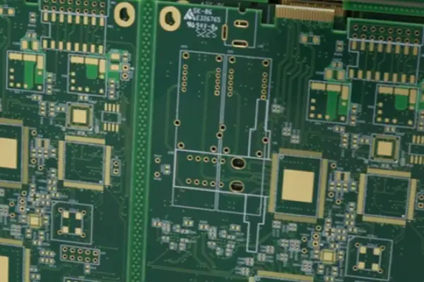
What Serious HDI PCB Manufacturers Actually Focus On
I have visited several factories producing high-end circuit boards and noticed an interesting pattern. The HDI PCB manufacturers who truly excel at this type of product rarely go around boasting about how impressive their technology is. Instead, they focus on details that sound unglamorous yet are extraordinarily demanding — such as how to ensure that after pressing together dozens of board layers, the impedance of the inner traces remains highly consistent; or how to control signal reflections when placing densely packed vias in an extremely limited space.
These things sound anything but exciting. But they are precisely what determines whether a board can run stably at high speeds.
Such manufacturers might spend several months optimizing the flow parameters of a special prepreg material to ensure uniform dielectric thickness during multilayer lamination. Or they might deeply study electroplating bath chemistry to achieve denser, more uniform copper deposition on deep via hole walls — reducing losses during high-speed signal transmission. These microscopic differences, amplified to the system level, translate into the difference between adequate and exceptional performance.
Why You Cannot Simply Integrate Everything Into the Chip
Someone might ask: given this complexity, why not use more advanced chips to integrate everything directly?
The problem is that 5G standards and application scenarios are still rapidly evolving. A design that is current today may require upgrading next year. If everything is locked into the chip, the cost would be prohibitive. A well-designed baseband PCB can actually provide a degree of flexibility — allowing adaptation to new requirements by replacing certain components. This places higher demands on designers: you must not only know how to address the present, but also leave space for possible future direction changes.
For example, reserving interface points and power supply arrangements for a future AI inference module, or pre-embedding some high-speed channels for subsequent bandwidth upgrades. This forward-looking design thinking requires engineers to have deep understanding of communication protocol evolution and semiconductor development trends.
The Trap of Extreme Physical Density
Many engineers receive a specification and immediately bury themselves in layout, trying to cram all chips into the smallest possible space. The result? DDR fails to run at its rated speed, or a critical synchronization signal is contaminated by power supply noise to the point of being unusable.
The problem is that they considered only integration in the physical sense while ignoring isolation in the electrical sense. A good baseband PCB design is more like planning the transportation and communities of a miniature city. You must let the financial district (high-speed data), the research district (precision clock), and the industrial district (high-power supply) be closely connected while not interfering with each other.
I recall a case shared by an HDI PCB manufacturer I worked with. A client submitted a very aggressive design using many blind and buried via techniques to minimize board area. But during prototype testing, the board consistently dropped packets. Everyone investigated and found that a critical voltage regulation module was placed too close to a group of high-speed serial differential pairs. The tiny ripple on the power supply was coupling into the data lines. Under high loads, this caused bit errors.
The solution was not to upgrade to more expensive board material. Instead, the layout was adjusted in a way that seemed to waste space — giving that power module a quiet zone of its own, with its filtering circuit optimized. The cost increase was minimal, but stability jumped immediately.
Stacking more layers and using ultra-fine traces is not always the optimal solution. Rational partitioning and shielding strategies, combined with careful ground plane design, often achieve more with less. What ultimately judges a board’s quality is its long-term stability and reliability in actual equipment — not how compact and high-tech it looks on the drawing.
The Digital Section Is Where the Real Engineering Challenge Lives
Many people assume that RF boards dealing with analog signals are more complex. But when you genuinely go deep into designing a modern communication device’s core processing board, you discover that the challenges of the digital world are an entirely different dimension.
Imagine needing to route dozens of groups of high-speed differential pairs in the space of a palm, each requiring strict timing relationships to be maintained. This is absolutely not something you can handle by simply drawing a few lines.
I have seen far too many projects fail to achieve full-system performance due to digital signal quality problems, spending months of debug time without finding the cause. In one 5G device development case, the system was consistently unstable under high load. After extensive investigation, the root cause was traced to an ordinary-looking circuit board. A critical clock signal line was run parallel to adjacent data lines for too long, producing severe crosstalk. At the same time, the board material’s dielectric constant fluctuated significantly with temperature — as the device heated up, signal transmission delay drifted.
After comparing several common high-speed board materials, I found that one model — although not the top performer in loss specifications — had special optimization in its fiberglass weave pattern. In actual testing, its eye diagram quality was better and jitter was smaller. This is why many professional manufacturers now develop specialized board material series for different application scenarios.
Layer Stack Planning: A Multi-Floor Functional Architecture
The first time I saw a twenty-layer board stack-up structure I was genuinely impressed — it was like designing a miniature skyscraper, with each floor having a clearly defined function.
How to arrange the power layers, how to partition the ground planes, which layer should carry high-speed signals, which should handle low-speed control signals — the depth of consideration required is enormous.
And you cannot only look at single-board performance. You must also consider the compatibility of the entire system. The interface between the baseband processing section and the RF front end is especially critical. Any slight impedance discontinuity or excessive crosstalk at that interface causes bit error rates across the entire link to spike.
We had one project where we initially used ordinary connectors to save cost. Testing revealed that data throughput in certain frequency bands consistently fell short of the theoretical target. Switching to a connector specifically designed for high-speed transmission — though considerably more expensive — immediately brought performance into specification. That is the classic example of details deciding success or failure.
Power Distribution Network: The Root Cause People Miss Most Often
Wireless baseband processors see enormous power consumption swings in operation. At times, the instantaneous current demand spikes to hundreds of amps. And the rate of change is extreme — the current may multiply several times within a single microsecond. This kind of instantaneous high current is an enormous test for the power delivery network. If poorly designed, voltage swings like a roller coaster and chips may crash directly.
Different capacitance values cover different frequency ranges. Large capacitors handle low-frequency fluctuations; small capacitors manage high-frequency transient changes. You must combine them and use them together — and placement matters enormously. Closer to the chip’s power supply pins is always better.
Some well-executed designs place the power layer and ground layer extremely close together — sometimes with only about 0.1mm separation. The purpose is to form a natural parallel-plate capacitor, providing the shortest possible return path for high-frequency transient currents.
Power integrity and signal integrity are mutually interactive. When the power supply is unstable, noise couples onto signal lines through shared paths, causing eye diagram closure or timing errors. Especially on 5G chips operating at very low supply voltages, even a few tens of millivolts of noise can cause the entire system to malfunction.
Manufacturing Is Where Theory Meets Reality
Many engineers arrive at HDI PCB manufacturers with perfect simulation reports, only for the manufactured boards to fail mysteriously in the field.
Dimensional stability control is one of the most painful problems. Microscopic errors accumulate across many layers during lamination and can push final registration tolerances beyond acceptable limits. For a board used in testing with dimensions approaching 400 by 120mm and thickness exceeding standard specifications, managing expansion and contraction through multiple lamination cycles required several rounds of process adjustment during trial production.
The material interface problem is equally important. Many wireless baseband PCBs are not made from a single material. If the stress between interface layers or the mismatch of thermal expansion coefficients is not properly managed, long-term reliability will suffer significantly. Some boards test normally at the start but show delamination or cracks after temperature cycling experiments.
Rather than endlessly chasing more aggressive material specifications, it is often better to first calibrate your press parameters properly. Different batches of resin may have different flow characteristics. Minor variations in copper foil surface roughness. These factors produce measurable effects on insertion loss at high frequencies — factors that were often overlooked in the lower-speed era.
Integration Is Not Always the Right Answer
Everyone now likes to pack various functions onto a single board, as though higher layer count and greater complexity signal more advanced technology. But when layer count increases, how do you handle thermal dissipation? How do you manage signal interference between different functional modules?
Sometimes simplifying the design actually delivers more reliable overall performance. Physically separating sensitive analog receive circuitry from digital processing and power management modules, with independent power layers and grounding strategies, is far more effective than piling everything together.
I explored what happens when AI inference modules are integrated directly into existing baseband board architectures. To power and cool that high-performance SoC, the multilayer PCB layer count was pushed to eighteen or more. The board became thick and rigid, more prone to problems in environments with vibration or large temperature variations — solder joint fatigue and subtle inner-layer delamination all emerged.
A more flexible modular design — where the core computational functions use a stable, proven platform and the rapidly iterating AI processing units are handled as separate, swappable cards — often delivers better long-term reliability. It reduces main board complexity while allowing the intelligence layer to be updated without disrupting the core digital foundation.
Finding the Right HDI PCB Manufacturer: What Specification Sheets Cannot Tell You
Selecting a PCB supplier is essentially selecting a business partner. You are not looking for a simple processing factory — you are looking for a team that can solve problems with you.
The right manufacturer will engage early in the design process. They will proactively flag which designs are theoretically perfect but will have low yield at mass production scale; suggest adjustments to avoid potential stress concentration; or explain why a specific signal routing approach will introduce practical EMI issues during manufacturing.
One of the best manufacturers I have worked with approached a situation where material supply became constrained with complete confidence — because they had established relationships with multiple upstream suppliers and maintained intelligent safety stock. Our project timeline was essentially unaffected while a competitor told their customer to wait two weeks.
On testing: many factories claim they can perform comprehensive testing, but actual execution is another matter entirely. True testing should run throughout the entire production process, from incoming material inspection through to finished product verification, with clear standards and data records at every step. For high-requirement products like wireless baseband boards, temperature cycling tests and long-term reliability validation absolutely cannot be skimped.
Real-world reliability is designed, manufactured, and tested into the board — not simulated into it. You must assume the board will eventually face all kinds of extreme conditions: dramatic temperature changes, continuous power-on and power-off cycling stress, the constant presence of moisture in the air. Then make your material and process selections based on those assumptions, and design your verification plan accordingly.
The Balance Between Ideal Performance and Real-World Robustness
Sometimes the greatest benefit that technical progress brings is not linear performance improvement — but the additional design margin and design freedom it provides. New materials and processes may allow routing to be somewhat more relaxed, eliminating the agonizing over saving every fraction of a millimeter of trace length. That additional margin ultimately translates into more stable product performance and longer service life.
For wireless baseband PCBs, you must always remember that this board will operate 24 hours a day, 7 days a week inside a base station. The environmental temperature will vary. The electromagnetic environment around it may be complex.
After your simulation software has the impedance perfectly tuned — have you considered that after the board material undergoes multiple reflow soldering cycles, its dielectric constant may shift slightly? Does your design have sufficient margin to tolerate that shift?
That is the core difference between an engineer and a pure theorist: we must find a solid balance between ideal physical models and the uncertainty-filled real world.
The companies that build the most reliable wireless baseband boards are almost never the ones chasing the most aggressive specifications. They are the ones who have internalized this lesson — and built their entire design and manufacturing process around it.
Have you ever wondered why your home internet speed fluctuates unpredictably? The
In the field of industrial automation, people often pay attention to AI
Ever wonder how your phone maintains a stable signal? It relies on
- Experto en producción de lotes pequeños y medianos
- Fabricación de placas de circuito impreso de alta precisión y montaje automatizado
- Socio fiable para proyectos electrónicos OEM/ODM
Horario comercial: (de lunes a sábado) De 9:00 a 18:30