

Laser Marking Machine PCB Signal Integrity Failures: Why Galvo Jitter and Ragged Marks Rarely Start With the Laser
A fiber laser marking machine that ran perfectly for six months can
I’ve always found circuit board making genuinely interesting. Early on, I tried doing it myself, and quickly discovered those sesame-seed-sized components can drive you absolutely crazy. Especially the 0402-package parts, where pad spacing is so tight a pin can barely fit through, let alone hand soldering. Once, stubbornly refusing to believe it couldn’t be done, I insisted on taking on a 0603-package component and ended up wasting an entire sheet of copper-clad laminate.
Looking back now, why fight yourself over it? Making a PCB by hand is inherently a process full of variables. I remember once using toner transfer to make a board — even though the printer had a freshly replaced toner cartridge, the transfer onto the copper board still kept breaking traces. It later turned out the iron’s temperature wasn’t uniform, and toner simply hadn’t pressed firmly onto the finer lines.
On pad sizing, I have a bit of practical wisdom: factory-made boards are indeed refined, but when doing it yourself, you need to leave generous margin. I generally make pads a few tenths of a millimeter larger than the original size, so even if drilling is slightly off, it won’t scrap the whole board.
As for via design, this is probably the most frustrating part of DIY circuit boards. Plated vias are basically impossible to achieve in a home workshop, so my habit now is to route everything on a single side as much as possible, reserving jumper-wire positions wherever a layer change is genuinely needed. It doesn’t look elegant, but at least it guarantees connectivity.
Sometimes seeing those beautifully finished miniature circuit boards online still tempts me, but after a few failures, I’ve become much clearer about exactly what scale I can handle. Now, if I run into a particularly fine-pitch design, I’ll go straight to a professional prototyping service — after all, time is a cost too.
Honestly, the most fascinating part of making a PCB by hand is that sense of imperfect authenticity. The satisfaction of successfully powering up a circuit each time is something factory prototyping simply can’t replicate. The key is finding a difficulty level that suits you — starting with simple through-hole components and gradually progressing is how you keep the passion alive.
Every time I see someone eagerly starting their first PCB, it reminds me of what I was like back then. Back then, I thought all it took was drawing the traces, transferring them to the board, and etching — done. What actually happened? That board was an absolute mess, traces broken in places, and several pads had fallen off entirely.
Actually, a lot of people underestimate the patience this DIY process requires. It’s not a simple copy-paste job — it’s a craft that requires repeated practice. The first time I tried, I used the toner-transfer method, fully confident that a few passes with an iron would do the job, only to find the toner adhered unevenly, and after etching, some fine lines simply weren’t there at all. I later understood that temperature control and pressing time both need to be dialed in through trial and error — there’s no shortcut.
The mistake beginners make most often is probably rushing — always wanting to get it right on the first try. I remember once, to save time, mixing the etching solution especially concentrated, and it over-etched the copper foil, leaving even the parts that should have stayed behind fragile enough to snap at the slightest touch. Making a PCB genuinely can’t be rushed — every step needs a solid, steady approach.
Then there’s drilling — don’t underestimate how simple it looks, because it demands real precision. If the drill bit wanders or you press too hard and the hole position shifts, soldering components afterward becomes a real headache, and you might have to redo the whole board. Now I always locate the position with a small drill bit first, then gradually widen the hole — it costs a few extra minutes, but it avoids a lot of problems.
The biggest challenge in DIY PCB work isn’t really the technique itself — it’s the mindset. Many people give up after one or two failures, but I’ve always felt that every failure helps you understand material characteristics better — things like copper-clad-laminate quality, transfer-paper type, even ambient humidity all affect the final result. Only through hands-on practice can you build the kind of experience that’s never written in a book.
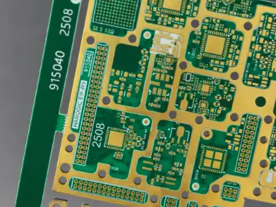
Now I actually recommend beginners start with a simple single-sided board — don’t jump straight into a complex double-sided or multilayer board. Get the basic process solid first, then gradually increase the difficulty. That way you keep your interest alive while genuinely seeing progress. After all, the sense of accomplishment from making your own working board is something you’ll never get from a store-bought one.
I’ve been making circuit boards by hand for several years now. Early on, I always assumed getting the traces right was all it took — until the first time I actually watched copper foil curl up under heat, I realized it’s nowhere near that simple.
I remember once spending two full days making a double-sided PCB. Drawing the design went smoothly, and the printout looked great, but the soldering stage turned into total chaos. The iron that day was an old, non-adjustable one borrowed from a friend, and the moment it touched the first chip pin, I smelled something burning — not the pleasant rosin smell, but the acrid smell of scorched plastic.
I later gradually came to understand that soldering is actually a job requiring a sense of rhythm. You need the iron tip to stay in contact with the pad for exactly the right amount of time — too short and the solder won’t melt, too long and you’ll lift the copper foil right off the board.
Now I’ve made a habit of applying a thin coat of flux to pads first with a small brush, especially for fine-pitch surface-mount components. This step gets overlooked by a lot of people, but it genuinely saves a lot of trouble. Flux doesn’t just help solder flow more smoothly — more importantly, it protects fine pads from oxidizing and turning black through repeated heating.
On temperature control, I now use a soldering iron with precise temperature adjustment. Different board materials actually need different temperatures — fiberglass board can handle higher heat than paper-based board, while flexible circuit boards need special care. Once, soldering a connector onto a flex board, I set the temperature 5 degrees too high, and the substrate near the connector visibly deformed.
What gives me the biggest headache is a chip with many pins, especially BGA packages where the pins sit underneath the chip. You can’t see the soldering condition at all — you’re going entirely by feel. That’s when flux becomes your lifesaver — you need enough of it, but not so much that it flows everywhere.
Inspection after soldering is also critical. I’ve made it a habit to look everything over with a magnifying glass first before powering it on. Sometimes a solder joint that looks perfect to the naked eye is actually just barely hanging onto the pin, and the slightest vibration can break the connection. This kind of problem is especially common in small-batch DIY work, since unlike a factory, there’s no automated optical inspection equipment — it all comes down to manual checking.
Now, every time I work on a new PCB, I set aside plenty of dedicated time for the soldering stage. This step genuinely can’t be rushed — the more you hurry, the more likely something goes wrong. Sometimes an entire afternoon might only get one complex chip properly soldered, but slow, careful work always beats rushing through it only to have to tear it all apart and redo it.
Every time I see online tutorials for making a PCB, I find them genuinely interesting, but only when you actually try it yourself do you realize it’s not that simple.
I tried using ordinary A4 paper for toner transfer once, and the result was an absolute disaster. Switching to the glossy backing paper from adhesive labels helped somewhat, but I still had to repeatedly adjust the temperature several times to find the right setting.
Speaking of temperature control, this is genuinely a skill. Too hot and the toner smears together; too cold and it won’t adhere properly. I tried using a clothes iron and found the temperature difference between the center and the edges was too large to guarantee even heating.
Actually, I think the etching step is the most critical. Many people assume mixing up some ferric chloride solution roughly right is enough, but if concentration control isn’t right, problems come up easily.
I remember once, rushing to finish quickly, I peeled the paper off right after transferring, and a large patch of toner came off with it.
Now I prefer using a modified laminator as my toner-transfer device — the temperature is much more stable. That said, I still always run a small test before starting any real job.
The most frustrating thing about making a PCB is broken traces or short circuits — sometimes it looks fine to the naked eye, and then the moment you power it on, something goes wrong.
At the end of the day, this is a skill you build through practice — nobody gets it perfect on the first try. Try a few more times and you’ll gradually pick up the tricks.
Sometimes failure actually teaches you more — like learning what temperature range works best for your equipment, or which etching solution gives the best results.
Looking back now at those early boards I made, they were genuinely a mess, but it’s exactly those experiences that helped me gradually work out a method that suits me.
The most important thing in doing this kind of work is patience — rushing only makes mistakes more likely. Now I always prepare all my materials in advance and leave plenty of time to work through it slowly.
Honestly, the joy of DIY work is in the process itself. The finished product might not be as refined as a factory-made one, but the feeling of making it yourself is completely different.
Every time I successfully make a working board, I feel a real sense of accomplishment, even if it took several days — it’s worth it.
I think anyone who enjoys hands-on work can understand this feeling — it’s about enjoying the process of creating something from nothing.
Of course, prototyping prices are so affordable these days that handing it straight to a factory might be more convenient. But the experience of doing it yourself is something money can’t buy.
Sometimes friends don’t understand why I spend so much time making boards myself, but they don’t get the satisfaction of creating something with your own hands.
Maybe this is what craftsmanship looks like — time-consuming and effortful, but the moment you see the finished product, it all feels worth it.
These days, I genuinely enjoy this slow, deliberate process — it feels remarkably stress-relieving.
If you’d like to try making a PCB yourself, I’d suggest starting with a simple single-sided board. Once you get comfortable, move on to more complex double-sided or multilayer boards.
Remember not to chase perfection too hard — getting it working on your first try is already quite an achievement.
I’ve recently noticed something interesting — many people treat PCB making as something that must be done entirely by hand. In reality, the most fascinating part of circuit design is the process of bringing an idea to life. I remember the first time I tried making a board with a sensor, I spent two days fiddling with it on my apartment balcony, and the traces still etched unevenly. I later sent the design file to a professional prototyping shop, and three days later received a finished product — the refined quality made me suddenly realize that handing certain steps off to professionals is actually the smarter choice.
Desktop-level equipment is genuinely becoming more accessible these days, but that doesn’t mean every step needs to be done yourself. Just as we don’t raise a cow ourselves just to drink milk, choosing the right tool and method for the job is what actually matters. This becomes especially clear when you need to iterate on a circuit repeatedly — that’s exactly when the value of rapid prototyping shows itself. Spending just a small amount of money gets you factory-grade process quality, which is far more efficient than repeated trial and error at home.
A hardware team I know once insisted on making every PCB themselves, and their project timeline fell seriously behind as a result. It wasn’t until they outsourced prototyping for a core board that they discovered the signal-interference problem that had plagued them for so long wasn’t a design flaw at all — it was a limitation of their DIY process. That experience gave me a deep appreciation for the fact that professional prototyping isn’t just about saving time — more importantly, it gives you a reliable process baseline. And for something engineered to run unattended for years — a Cell Tower Power Supply PCB out on a remote tower site, for instance — that reliable baseline isn’t optional at all.
Of course, making simple circuits by hand is still a great way to learn. But when you need to implement complex functionality, handing the prototyping stage to a professional service lets you focus your energy on the circuit innovation that actually matters. After all, our goal is to build a good product, not to become an all-around craftsman. This kind of division of labor actually lets an individual creator produce more professional work.
Sometimes choice matters more than effort. Using the right production method at the right stage might be exactly the wisdom behind mastering circuit design.
When it comes to making circuit boards by hand, I think what gives people the biggest headache isn’t drawing the layout or etching the copper — it’s actually the steps that look simple that trip you up most easily. Take drilling, for example — a lot of people assume grabbing any old hand drill will get the job done.
I made this exact mistake when I first started — I only had a few standard-size drill bits on hand and just pushed forward anyway. What happened? Either the hole came out too large and ate away most of the pad edge, or I pressed too hard and snapped a fine drill bit right inside the board — the kind of moment that makes you want to throw the whole thing in the trash. I gradually came to understand: making a PCB really isn’t something you can wing.
Choosing the right tool matters enormously — especially for holes under one millimeter in diameter, which genuinely require patience and accumulated experience. For drilling IC pin holes, for example, it’s best to use a fine carbide micro drill bit in the 0.1 to 0.3mm range — a precision tool set with an interchangeable-head handle is genuinely useful, since these bits are both more durable and far more precise. Of course, if you’re only making one or two boards occasionally, you can also thread thin wire through an un-drilled hole and solder it in place — more of a hassle, but at least it guarantees you won’t ruin the whole substrate through an operating mistake.
I’ve also found that a lot of people overlook one detail: lightly punching a small dimple at the center of each pad with a manual center punch before drilling is genuinely worthwhile — it effectively prevents the drill bit from sliding off-center when it starts. After all, alignment that looks fine to the naked eye doesn’t mean there won’t be a tiny deviation during actual machining.
Finally, a word on speed control: too fast and you burn out the drill tip’s lifespan; too slow and you hurt cutting efficiency — so finding the right range matters. Personally, I prefer a medium speed paired with gentle, even downward pressure to work through the process — that protects the tool while still getting a good result. In short, doing a circuit board well starts with taking these seemingly unremarkable details seriously. Handle every step carefully and you’ll hit far fewer detours, and get to enjoy that moment when the finished board lights up that much sooner.
While making circuit boards by hand, I’ve noticed something interesting — a lot of people focus all their attention on precisely controlling the etching process. In reality, what genuinely determines success or failure is the most easily overlooked step: the quality of the toner transfer.
I remember the first time I tried, I used an ordinary laser printer, and the result was mediocre — the trace edges always came out rough. It was only after switching to dedicated transfer paper that I understood why veterans always emphasize this detail. Traces that look complete to the naked eye are actually riddled with tiny gaps under a microscope, and those spots become breakthrough points during etching.
On mixing the etching solution, I actually have a different take. As a beginner, I also strictly weighed everything by ratio; now I trust my own observation more, since every batch of material has different activity levels. For example, the last batch of ferric chloride I used was noticeably stronger than what I had six months ago, so I appropriately reduced the concentration. The key is keeping the liquid flow even.
Temperature control genuinely takes some experience. When making boards in winter, I like keeping the container in a basin of warm water to maintain a constant temperature; in summer, I avoid direct sunlight. Once, not paying attention to ambient temperature, the etching speed spiraled out of control and the traces ended up thinner than a strand of hair.
The most frustrating step is film removal — press too hard and you damage the copper foil, too light and residue is left behind. I’ve now found a clever workaround: soften the toner with warm water first, then gently roll a cotton swab over it to wipe it away. This protects the traces while cleaning thoroughly.
Honestly, the most fascinating part of making circuit boards is running into a new problem every time. Last week I solved over-etching at the corners; this week I found bubbles tend to form around the vias. This ongoing process of solving one problem after another is more satisfying than simply succeeding once.
At the end of the day, hand-fabrication itself is an art form — chasing absolute perfection actually kills the enjoyment. What matters is finding the rhythm that fits you within a controllable range. I’ve even come to enjoy those small imperfections now — they give each board its own unique character.
Every time I see a beginner eagerly starting to make a circuit board, I get a little worried. Many people assume that once the traces are drawn correctly, it’ll simply power up and work — but reality often turns out otherwise.
I made plenty of mistakes myself when I first got into circuit-board making, and the most obvious one was overlooking the importance of detail. For instance, during soldering, letting two pins get too close together causes a short circuit — and once that happens, at best a single component fails, at worst the entire board is scrapped.
Once, I helped a friend check a self-made audio amplifier board. He complained it smelled like it was burning the moment he powered it on. Looking closely, I found a capacitor installed with reversed polarity, plus obvious solder-residue buildup near the power circuit — a classic result of inadequate visual inspection.
Actually, the thing to fear most in making circuit boards is rushing to finish. Some people like soldering every single component in one go before testing — that approach carries real risk, because once something goes wrong, it’s hard to quickly pinpoint exactly where the error occurred.
My habit now is to work in stages — solder the power section first, confirm voltage stability, then gradually add other functional modules. That way, even if something isn’t working right, the troubleshooting scope is much narrower.
Also, many people easily overlook tool selection — for example, using ordinary tweezers to adjust tiny surface-mount components, or not having a proper magnifying glass to check solder-joint quality. These seemingly minor details often determine success or failure in the end.
One more point is about component selection. Some people, chasing miniaturization, choose extremely small packages, which makes hand soldering genuinely difficult and actually increases the odds of a mistake. I generally recommend beginners start practicing with larger-sized components first, then try more fine-pitch designs once they’re comfortable.
At the end of the day, making a circuit board isn’t just a technical skill — it tests patience and attention to detail just as much. Every failure is really an accumulation of experience — as long as you learn the lesson, you’ll do better next time.
I’ve always found it genuinely interesting that people still make circuit boards by hand today. Many might feel it’s too time-consuming — and it does take real effort. But I’ve found this process lets you truly understand how a circuit becomes a physical object, step by step. From schematic design to PCB layout to actual fabrication, every stage requires considering practical issues like current-carrying capacity and signal integrity — details that are hard to fully appreciate in simulation software alone.
I remember being especially nervous the first time I tried making a board with toner transfer. My hands were shaking as I placed the printed design onto the copper board. By the time etching started, I was even more careful, terrified of making a mistake. Even though the final product had somewhat rough edges, seeing the traces I designed appear clearly in front of me gave a genuinely special sense of accomplishment. Especially when testing continuity with a multimeter, hearing that beep confirming the circuit was connected — all the effort suddenly felt worth it.
Plenty of fast, cheap prototyping services can be found online today. But I still enjoy occasionally making a board by hand, especially for small experimental circuits. Through the DIY process, you discover a lot of design issues you wouldn’t have noticed otherwise — things like insufficient trace width or pads that are too small. Once, a power trace I designed was too thin, and it noticeably heated up once powered on — that experience gave me a much deeper understanding of the relationship between trace width and current.
One time, I helped a friend repair an old piece of equipment that needed a discontinued circuit board replaced. We tried making it ourselves and found some aspects of the original design weren’t quite reasonable, so we improved the layout along the way. It took a whole weekend, but fixing it felt even more satisfying than simply buying a new board. We even added an overcurrent protection circuit on top of the original functionality, making the old equipment safer and more reliable to use.
Of course, I’m not saying every situation is suited to DIY. Complex multilayer boards, or anything requiring high precision, definitely calls for a professional manufacturer — the kind of specialized multilayer pcb manufacturer o high Frequency PCB supplier that has the equipment and process control a home setup simply can’t match. But for learning and experimentation, going through the entire process from drawing to physical object teaches you far more than theory alone. Things like adjusting layout based on component size, or arranging component spacing with thermal considerations in mind — these are skills you only truly master through hands-on practice.
I think making circuit boards yourself these days is more like a way of keeping your hands sharp. It’s a bit like a chef occasionally preparing a meal entirely from scratch instead of always relying on pre-made ingredients. Every board you finish gives you a fresh understanding of circuit design — an experience no amount of tutorial-watching can replace. Especially when you need to quickly validate an idea, DIY fabrication lets you see a physical result within hours.
Honestly, once you’ve done enough of it, you realize the hardest part of DIY work isn’t the technique — it’s the patience. Sometimes a single small mistake means starting over from scratch, but every failure helps you remember one easily overlooked detail. This kind of learning is slow, but it’s genuinely solid. For example, drilling off by just a fraction of a millimeter can prevent a component from mounting properly — a lesson that makes you pay much closer attention to dimensional precision in future designs.
When I teach students now, I also suggest they make a few boards by hand before considering going straight to professional prototyping. Because only by personally experiencing toner-transfer temperature control and etching-time judgment will they truly understand which design details affect the fabrication outcome. This kind of experience is especially useful for future design work. I often have students compare a hand-made version of the same board against a factory-prototyped version — by comparing pad precision and trace-width consistency, they get a much more intuitive understanding of how process requirements shape design.
Every time I see someone enthusiastically getting ready to make a PCB, I can’t help wanting to offer a few reminders. Many people jump straight into design software, draw out the circuit, and assume connecting the traces is all it takes — but there’s a detail that’s especially easy to overlook: trace width.
I’ve seen quite a few beginners directly apply factory-grade parameters to a board they’re making by hand, and you can imagine the result: traces as thin as a strand of hair either fail to transfer at all, or snap the moment you’re careless during etching. This really isn’t their fault, because most tutorials focus on how to draw the layout and rarely mention the subtle but critical differences that come up during actual fabrication.
Another common misconception is assuming that once the traces are drawn, the rest of the steps are all roughly the same. In reality, every process step has its own temperament — for example, if your copper-clad-laminate thickness differs, etching time needs to be adjusted accordingly, or you’ll easily get side-etching that eats away even the traces meant to be preserved. Once, I used the wrong copper-foil thickness — even though my design had plenty of trace width, the finished trace ended up much thinner than expected, nearly ruining the entire board.
Drilling is another step people shouldn’t underestimate. Many assume grabbing a hand drill and punching a few holes is enough, but even a slight position deviation makes soldering components afterward genuinely painful. Once, trying to save effort, I skipped using a drill press, and several dual-row headers ended up misaligned, forcing me to force them into place — the board’s lifespan was probably significantly reduced as a result.
At the end of the day, the biggest challenge of making a PCB yourself isn’t the technique itself — it’s how you combine design with process. You need to think through, ahead of time, what could go wrong at every step, rather than tracing back the cause only after a failure. For example, when drawing the layout, you need to consider how fine a trace your transfer paper can actually handle, and how to control etching-solution concentration — these details often matter more to success than the circuit design itself.
Of course, this process genuinely teaches you a lot. Every mistake is a lesson, and gradually you’ll build up your own experience, learning exactly which parameters work best for your tools and materials.
A fiber laser marking machine that ran perfectly for six months can
A Microgrid Controller PCB kept showing signal jitter during grid-tied testing, and
After years of building PCs, I’ve noticed that most people obsess over
- Experto en producción de lotes pequeños y medianos
- Fabricación de placas de circuito impreso de alta precisión y montaje automatizado
- Socio fiable para proyectos electrónicos OEM/ODM
Horario comercial: (de lunes a sábado) De 9:00 a 18:30
Get quote, solution or any question, Andre always here to help