
Heat Dissipation Challenges and Solutions in PCB Circuit Board Design
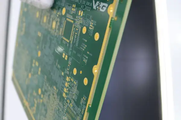
Circuit boards are more than just that green board in a phone
Recently, while looking through some old electronic devices, I suddenly realized something: why are modern mobile phones so thin? Upon disassembling them, I discovered that the circuit boards inside were exquisitely crafted, almost like works of art. This transformation is largely attributed to the development of HDI technology.
I remember seeing circuit boards covered in thick, robust lines when repairing mobile phones ten years ago; now, they have evolved into fine meshes visible only under a microscope. This transformation represents not just technological advancements, but a revolution in design philosophy across the entire electronics industry.
Once, I visited a friend’s factory and saw them producing a special type of HDI PCB board. Workers had to wear protective suits and operate in a cleanroom. This level of precision manufacturing reminded me of the work of Swiss watchmakers, where every step requires extreme focus.
Many people may not know that the smartphone functions we take for granted today, such as facial recognition and high-speed charging, rely on these seemingly insignificant circuit board technologies. Without sufficiently precise wiring design, even the most powerful chip cannot reach its full potential.
I particularly admire those technical teams that dare to break with convention. They are not satisfied with existing manufacturing standards but constantly explore more advanced possibilities. Like the Ultra-level processes some manufacturers are now experimenting with, this completely transcends the scope of traditional circuit boards; it’s more like microscopic architectural engineering.
Interestingly, technological advancements often lead to unexpected applications. For example, the miniature sensors used in medical devices or the control modules of autonomous driving systems in cars—these fields have much stricter reliability requirements for circuit boards than consumer electronics.
Sometimes I think that in a few years, when we look back at today’s technology, it might seem primitive, but it’s precisely this spirit of continuous breakthroughs that drives the entire industry forward.
Whenever I see circuit designs that pursue ultimate performance, a question always comes to mind: Are we focusing too much on parameters? Especially in the design of circuit boards used in critical equipment, such as HDI PCB boards, engineers often expend a lot of energy for a few percentage points of performance improvement.
I’ve seen many design teams, when choosing HDI technology, immediately stack more layers to pursue finer linewidths. However, this approach doesn’t necessarily yield the best results. Once, while working on a medical equipment project, we found that appropriately reducing the number of interconnect layers actually improved signal integrity because it simplified the transmission path of high-frequency signals. For example, in the design of the control board for an MRI machine, we streamlined the 12-layer board to 8 layers, reducing signal reflections by optimizing the wiring topology. Actual measurements showed a 15% reduction in signal overshoot.
Power module design is prone to pitfalls. Many believe that using the thickest copper foil solves the high-current problem, but in practice, the heat dissipation bottleneck often lies in the dielectric layer, not the conductor itself. I recall a car charger project that initially used 10-ounce thick copper foil, only to find the thermal failure point on the FR4 material. Switching to thinner copper foil with a metal substrate truly solved the problem. Specifically, we used 2-ounce copper foil with an aluminum substrate, and thermal simulations showed a 22°C reduction in junction temperature compared to the original design, while simultaneously reducing weight by 30%.
The most easily overlooked aspect of Fabricación de PCB is material compatibility, especially when the design needs to handle both high-speed signals and high-power transmission. Simply pursuing high performance parameters can introduce hidden dangers. In a communication base station power supply project, we attempted to integrate digital control and power conversion on the same board, only to find that the heat dissipation paths interfered with each other. Ultimately, we had to separate them into two boards connected by connectors, increasing size but significantly improving reliability. In this case, the difference in thermal expansion coefficients between the TG170 board in the digital section and the ceramic substrate in the power section caused stress concentration at the solder joints. Separating the boards and using flexible wiring resulted in better thermal management.
Many engineers now associate high-density interconnects with laser drilling. However, in certain scenarios, mechanical drilling combined with via filling is more economical and practical, especially for power modules that need to carry high currents. Overly dense microvia arrays can weaken current-carrying capacity. I prefer to use a mix of drilling methods with different aperture sizes depending on the current. For example, in server power supply design, 0.3mm mechanical drilling with copper filling is used for paths with currents above 5A, while 0.1mm laser microvias are used for signal lines. This ensures current carrying capacity while controlling drilling costs.
The real test of design skill lies in balancing interconnect density and power density within a limited space. Sometimes, designs prioritize miniaturization by squeezing signal and power lines together. Although HDI technology is used, electromagnetic compatibility (EMC) tests frequently fail. Good design should provide appropriate spacing between lines with different functions, much like urban planning. In practical design, the concept of a “signal corridor” can be adopted. For example, in the layout of a smartwatch motherboard, an isolation area is reserved for the RF module, and power lines are grounded. This way, even with a line spacing of only 0.1mm, radiated emission tests can be passed.
My recent involvement in a new energy vehicle project has given me a new understanding of power electronics. The sampling circuit in the battery management system needs to handle weak signals while withstanding high-voltage isolation, which places high demands on the PCB’s insulation materials and structural design. We ultimately chose a solution of locally thickening the dielectric layer in critical areas, rather than using expensive materials for the entire board. This targeted design controlled costs while meeting safety standards. In practice, the PP dielectric layer was increased from 0.1mm to 0.4mm in the 1000V withstand voltage area, while maintaining the standard thickness in other areas. This only increased the board cost by 18% while achieving the 8mm creepage distance required for UL certification.
Ultimately, there is no standard answer to PCB design. The key is understanding the trade-offs behind each technology choice. For example, HDI technology can indeed improve integration, but it also brings increased costs and yield challenges. My experience is that preparing several alternative solutions for rapid verification at the beginning of a project is much more efficient than patching things up later. For example, in a recent IoT gateway project, we simultaneously conducted prototype tests on three solutions: through-hole, blind/buried via, and arbitrary layer interconnect. We ultimately found that for this application scenario, using a 4-layer board with selective immersion gold processing achieved the best balance between performance and cost. I’ve been pondering something lately: everyone’s been talking about how amazing and advanced HDI technology is. It’s true! It’s made a significant contribution to the miniaturization of electronic devices. But I think many people are overlooking a crucial point—what truly determines the quality of an HDI PCB board isn’t those fancy specifications, but rather the most basic process control.
I remember visiting a factory last year, and I was struck by the sight of an experienced worker in the workshop meticulously inspecting circuitry with a magnifying glass. He told me that many manufacturers are pursuing ever-smaller apertures in pursuit of layer thickness, neglecting the most basic alignment accuracy. The result is lower yield rates and higher rework costs.
In fact, building HDI is like assembling a building with blocks; it’s not about using more or more advanced blocks to create a more stable structure. Sometimes, overly complex structures can become a burden. I’ve seen designs where the dielectric layer is made extremely thin to stack more layers, leading to delamination during thermal stress testing.
There’s a misconception in the industry that intelligent equipment solves all problems. But the reality is that even the most advanced machines still require people with process knowledge to operate them. I once witnessed a fully automated production line scrap an entire batch of boards due to a simple missetting of lamination parameters. What does this illustrate? Even the most advanced technology cannot function without human experience and judgment.
Speaking of environmentally friendly materials, this is also a topic worth discussing. While halogen-free materials are certainly advantageous, their thermal stability is often inferior to traditional materials. Finding a balance between environmental requirements and performance requires engineers to have a deeper understanding of material properties, rather than simply following trends.
I believe the key to the future development of HDI lies not in blindly pursuing higher density, but in making existing technologies more stable and reliable. After all, users of electronic products don’t care how many layers you use; they only care whether the equipment can operate stably for three to five years.
Sometimes the simplest solution is the most effective. For example, improving heat dissipation design is more effective than simply pursuing high thermal conductivity materials in solving practical problems. This reminds me of a project I worked on before, where the team spent a lot of time researching new composite materials and finally discovered that adjusting the wiring layout could reduce the operating temperature by 15%.
Ultimately, good HDI design should be an art of balance—finding the optimal combination between density and reliability, cost and performance. This might be more meaningful and better reflect the value of engineers than simply pursuing technical specifications.
Every time I see HDI boards in precision instruments, I’m reminded of my childhood experience disassembling radios. Back then, I had no idea about micron-level precision; being able to solder components with a soldering iron was already a feat. Thinking about it now, those crooked solder joints would probably be impossible to transmit a signal on today’s HDI boards.
Actually, the most troublesome part of PCB design isn’t the circuit design itself, but ensuring that so many layers align perfectly. Once, I visited a factory and witnessed them performing alignment checks after lamination. A worker pointed to the image on the X-ray machine screen and said that the current requirements are as strict as one-third the diameter of a human hair. Looking closer, I realized that those hair-thin lines indeed require extreme precision. For example, in high-density interconnect boards with more than 10 layers, the interlayer alignment deviation must be controlled within 20 micrometers; otherwise, drilling might cut critical signal lines. Factories now commonly use optical positioning systems, etching precise alignment targets on each core layer and then using a CCD camera for multiple calibrations. Even so, during the high-temperature, high-pressure lamination process, differences in the thermal expansion coefficients of materials can still lead to micron-level displacements. This necessitates engineers considering thermal compatibility during the initial material selection phase.
Speaking of solder mask, I’ve found that many engineers underestimate its importance. Especially when dealing with micro-components like 01005, a misalignment of the solder mask layer exceeding 25 microns can render the entire board unusable. I recall our team once reworked a medical device HDI board three times due to precision issues with the solder mask windowing. In fact, the solder mask layer not only needs to precisely cover non-pad areas, but its thickness uniformity directly impacts soldering yield. Too thin a layer leads to insulation failure, while too thick a layer can cause tombstoning during micro-component soldering. High-end equipment now uses laser direct imaging technology to create solder mask patterns, improving precision to the 5-micron level and allowing for real-time thickness monitoring to adjust coating parameters.
More and more manufacturers are now using dry film solder mask to replace traditional ink processes. While this approach is more expensive, it is undeniably more reliable when handling ultra-fine pitch components. In a previous project, we needed to create 0.2mm BGA packages, and we solved the problem of easily broken solder mask bridges using dry film technology. Dry film solder mask, through vacuum lamination, can form a more uniform protective layer, and its dielectric constant stability is about 15% higher than liquid ink. Especially when dealing with CSP packages with a pitch of less than 0.3mm, dry film can create solder mask bridges only 30 micrometers wide, while traditional ink processes are close to their limit at 50 micrometers. However, dry film requires extremely high substrate surface flatness; any unevenness exceeding 5 micrometers can lead to incomplete lamination.
Choosing the surface treatment method also requires extreme care. While electroless nickel-palladium-gold plating is effective, improper thickness control can cause more problems. I’ve seen people try to save money by making the gold layer only 0.02 micrometers thick, and the boards oxidized after only six months in storage. You really can’t cut corners in this kind of situation; the required thickness must be maintained at every step. Taking the ENIG process as an example, the nickel layer needs to be stable at 3-5 micrometers to effectively block copper diffusion, while a gold layer thickness below 0.05 micrometers will result in pinhole defects. Currently, some automotive electronic boards with extremely high reliability requirements add a 0.2-0.5 micrometer palladium layer below the gold layer as a diffusion barrier. Although this increases costs by 20%, it can extend the solder joint lifespan by more than three times.
Material selection is also a complex matter. Once, we tested more than a dozen substrates for a high-frequency project and finally found that ordinary FR4 had more than three times the loss at high frequencies compared to specialized materials. This experience taught me that sometimes spending more on materials can save on later repair hassles. For example, in a 77GHz automotive radar board, we ultimately chose the Rogers 4350B substrate, which has a loss factor of only 0.0037 at 10GHz, while ordinary FR4 reaches 0.02. More importantly, the temperature coefficient of the dielectric constant of the specialized high-frequency materials can be controlled within ±50ppm/°C. This means that signal phase stability can be maintained within 3% over an operating temperature range of -40°C to 125°C.
Looking at these precision circuit boards now feels like looking at a miniature city. Each line is a street, each via is an overpass, and the resistive layer is the city’s green belt—it can’t take up too much space, yet it must provide the necessary isolation. This ingenious design always makes me feel the charm of engineering.
Ultimately, making a good HDI board requires not only technical parameters, but also a dedication to detail. Sometimes, a difference of just a few micrometers can drastically alter the product’s lifespan. This pursuit of excellence is perhaps the most valuable quality in our industry.
I’ve seen too many engineers treat HDI design as purely software manipulation. They think that once the circuit diagram is drawn, everything is fine, and they only rush to contact the manufacturer to fix problems when prototyping occurs.
In fact, the most important thing is flexibility in the design phase. In a previous project, we needed to fit over two hundred connection points into a space the size of a fingernail. We tried three different microvia arrangements before finding a balance. Sometimes, what you think is the optimal stacking method can be rendered useless in actual production due to material expansion coefficients.
Now, when I communicate with factory workers, I directly ask about the precision limits of their equipment for microvias. Once, they mentioned that their laser drilling machine’s yield rate dropped to 70% when processing microvias smaller than 0.1mm, which prompted us to decisively adjust our design.
Many people easily overlook the deformation of HDI boards at different temperatures. I once handled an eight-layer board that tested perfectly in the lab, but during mass production, the temperature difference in the lamination process caused misalignment of the inner layer microvias, rendering the entire batch unusable.
Instead of rigidly adhering to design specifications, it’s better to leave room for flexibility. Once, we deliberately increased the spacing of critical lines by 20%. Although the theoretical density decreased, the yield actually increased by 30%.
What’s truly important is understanding the underlying logic of manufacturing processes. For example, why certain substrate materials are better suited for deep blind vias, and why high-frequency signal lines must avoid specific via arrangements. These details are often more valuable than rigidly adhering to design rules.
Recently, while working on an automotive electronics project, I discovered that heat dissipation requirements completely change microvia layout strategies. The traditional dense stacking method used in fiber optic communication boards simply doesn’t work next to power devices. This made me rethink the fundamental meaning of high-density interconnects (HDI).
Ultimately, HDI design isn’t about pursuing parameter limits, but about finding a delicate balance between performance, cost, and manufacturability.
I’ve always felt that many people have a misconception about HDI boards—overly focusing on the numbers on the material specification sheets while ignoring the dynamic balance in practical applications. Take copper foil, for example. While the roughness data measured in the lab is important, what truly determines success or failure is often its adaptability within a specific stack-up structure.
Last year, a smart wearable project left a deep impression on me. The client insisted on using a particular ultra-low roughness copper foil, resulting in delamination during repeated bending tests. Later, they switched to rolled copper foil, which, although with a slightly higher surface roughness, tripled the flexibility life. This made me realize that the quality of materials cannot be judged without considering the application scenario, just as running shoes cannot be judged solely on breathability while ignoring cushioning requirements.
The stack-up design of HDI boards is more like assembling a 3D jigsaw puzzle. Once, we tried to cram six differential pairs into a 1+N+1 structure; the flowability of conventional prepreg was simply insufficient to handle the densely packed laser aperture areas. Later, we switched to a two-stage lamination process: first, filling the laser aperture cavities with a high-resin-content PP sheet, and then performing the main lamination, which achieved better dielectric uniformity.
The real test of design skill is actually the power supply integrity layout. I’ve seen too many cases where all the effort was spent on signal layer optimization, resulting in insufficient chip power supply and a decline in overall board performance. Now, when planning the stack-up, we simulate current loops in advance, and when necessary, we even allocate a separate adjacent ground layer for the power layer. This seemingly wasteful approach often results in more stable operation.
My recent experience with automotive radar board projects has once again broadened my understanding. In the millimeter-wave band, the losses caused by copper foil roughness are more severe than anticipated. However, simply pursuing a smooth surface can affect bonding strength. Ultimately, we found a new balance between roughness and adhesion by adjusting the browning treatment parameters. This practice of constantly breaking conventional wisdom is the most fascinating aspect of the HDI field.
In the end, an excellent HDI board is not a product of simply piling up parameters, but rather a designer’s comprehensive understanding of various factors such as current path, thermal management, and mechanical stress. Just like a master chef doesn’t rigidly adhere to a recipe but adjusts the heat according to the characteristics of the ingredients, this dynamic adjustment wisdom is the true core competitiveness.
I’ve always found the quality control of HDI boards particularly interesting. Many people may not understand the intricacies behind it.
I remember once receiving a batch of sample boards that all looked quite neat. But when we started cross-section analysis, we discovered quite a few problems. For example, some boards had micro-cracks at the interlayer bonding points, problems that are impossible to detect with the naked eye.
Speaking of the testing phase, I think the most challenging are the long-term stability tests. This involves placing the board in a high-temperature, high-humidity environment with continuous power and observing its performance. This process is particularly revealing of a board’s true quality.
I’ve seen boards that perform well initially in testing, but problems gradually emerge over time. For example, insulation performance deteriorates, or subtle leakage occurs. These require sophisticated instruments to detect.
Evaluating the quality of an HDI board cannot be based solely on a single indicator. Sometimes, individual tests may all meet standards, but problems still arise when used together. It’s like cooking: every ingredient is in the right amount, but the flavor is still off.
I prefer to carefully observe the minute details during the slicing process. For example, is the copper thickness of the vias uniform? Are there air bubbles or voids in the filler material? These seemingly insignificant details often determine the overall lifespan of the board.
Many manufacturers are now pursuing thinner boards, but I believe thickness is not the only standard. The key is to find a balance between thinness and durability. While excessively thin boards save space,
I’ve seen too many people overcomplicate HDI board issues. Often, the problem lies in the most basic aspects—such as the seemingly high-end cleanroom environment.
Last year, a customer complained about inexplicable short circuits on their HDI PCB boards. They had spent a lot of money upgrading their equipment but neglected basic workshop management. When I visited the site, I understood immediately—the so-called cleanroom wasn’t even following basic changing procedures. Workers in ordinary work clothes brought in more dust than the street outside.
The truly critical issues are often the easily overlooked details: the frequency of operator glove changes, the management of material transfer windows, and even the floor cleaning methods all affect the final result. For example, during micro-hole metallization, sweat residue on gloves can alter the surface tension of the plating solution, leading to uneven plating within the holes. If a negative pressure difference isn’t maintained at the material transfer windows, fibrous dust brought in by external airflow can adhere to the dry film surface, causing development defects. Even more insidious is floor cleaning; if highly volatile cleaning agents are used, the rising vapor can condense into an invisible liquid film on the low-temperature board surface, affecting the depth of focus accuracy of laser drilling.
When it comes to failure analysis, many people’s first reaction is to use high-end instruments. However, in my experience, reviewing process flow records often yields clues. In a recent case, comparing temperature and humidity records revealed that failures were concentrated during the rainy season. Although the workshop was labeled a cleanroom, the dehumidification system was inadequate, leading to abnormal chemical concentrations. Specifically, sodium carbonate in the developer solution accelerates carbon dioxide absorption when humidity exceeds 60%, with the effective concentration decreasing by 15% weekly, directly causing jagged edges on the circuitry. Another copper plating case showed that fluctuations in ambient humidity caused palladium colloids in the activator to flocculate, ultimately resulting in backlight testing showing poor light transmission at level 3 or higher.
Many manufacturers now blindly pursue certification levels, forgetting that the essence of a cleanroom is continuous maintenance. We have a supplier we’ve worked with for three years whose cleanroom level isn’t the highest, but they conduct complete particle count tests every quarter. This pragmatic attitude is more important than simply having high-level certifications. Their red, yellow, and green three-color early warning mechanism is particularly noteworthy: a yellow alert is triggered when the number of 0.3μm particles exceeds 80% of the standard value for two consecutive hours, immediately activating the backup fan; if metal particles larger than 5μm are detected simultaneously, the alert is upgraded to red, automatically isolating the relevant work sections and tracing the product batch within the past two hours.
In fact, the biggest fear in HDI manufacturing is assuming that investing in high-end equipment will solve all problems once and for all. What’s truly needed is maintaining sensitivity to every step, from material storage to personnel training—a tightly interconnected system. For example, if the substrate of vacuum-packed materials is not resealed within 4 hours after unsealing, its surface oxide layer will increase from 0.8nm to 2.5nm. This tiny change can cause the taper angle deviation of laser drilling to exceed 5 degrees. Furthermore, if new employee training neglects to teach them how to identify anti-static wrist strap failures—such as observing whether the wrist strap monitoring light exhibits regular, weak flashing—random open-circuit problems may not be exposed until impedance testing three months later.
Sometimes the simplest improvements are the most effective. For example, adding real-time monitoring screens to key processes allows operators to visually see changes in environmental parameters. This immediate feedback is far more useful than post-event analysis. Our temperature and humidity dashboard in the laser drilling room is a prime example: when the screen background changes from blue to yellow, operators automatically adjust equipment compensation parameters to keep the hole wall roughness below 0.8μm. Similarly, the countdown timer for the lifespan of the copper plating solution allows employees to anticipate additive failure 15 minutes in advance, increasing the first-time problem interception rate by 40%.
Ultimately, quality control is not about piling up technical specifications, but about establishing a work habit of full participation. When everyone realizes that their actions affect the final product, expensive testing equipment becomes a backup plan. Like our one-minute self-inspection method: before shift handover, operators use their mobile phones with macro lenses to photograph three sample areas; by comparing color differences, they can detect early signs of solution activity decay. This method of transforming professional judgment into intuitive perception reduces the average time to detect process anomalies from 6 hours to 20 minutes.
Having worked on HDI boards for so many years, I’ve come to a slightly different conclusion—sometimes obsessing over parameters can lead to neglecting real-world application scenarios. Take core board thickness, for example. I’ve seen too many engineers obsessively pursue theoretical values only to stumble at the fundamentals.
Last week, a customer brought in a solution they claimed was optimized to the extreme, but it simply wouldn’t run on a typical factory’s production line. Those precisely calculated thin core boards can indeed improve performance, but the reality is that most production lines simply can’t handle such delicate materials. Every time I see a core board as thin as a cicada’s wing getting deformed in the etching machine, I feel like they’re pushing the limits of physics.
The truly reliable approach is to thoroughly understand the manufacturer’s actual capabilities first. We once tried setting the dielectric layer spacing of the HDI PCB board to around 75 micrometers. Although it was more conservative than the theoretical optimal value, it was more stable. This design directly increased the yield by 15 percentage points when mass-producing eight-layer boards.
Regarding testing, I prefer a combination of methods instead of single-point testing. For example, when performing impedance testing, don’t just focus on the fluctuations in the TDR value. One board passed all individual tests, but after actual installation, it consistently experienced high-frequency signal loss. It was later discovered that the dielectric constant of the core boards varied slightly between different batches. This kind of problem requires comparing the impedance curve with the actual waveform to pinpoint the issue.
Now, I get a headache seeing orders that demand top-tier parameters from standard factories. I once had an order where the client insisted on extreme parameters, resulting in a third of the boards being stuck in the etching process during mass production. Ultimately, we switched to a slightly thicker core board, which theoretically reduced performance by 5%, but the cost dropped by 40%, and we delivered two weeks ahead of schedule.
Making HDI boards is actually quite similar to cooking—not every kitchen is suitable for molecular gastronomy. Instead of forcing all factories to handle ultra-thin materials, it’s better to adjust the design approach based on the actual production line. After all, a good design is one that can be stably mass-produced; lab-level parameters are just for reference, and applying them directly to the production line often results in disaster.
Recently, when working on six-layer blind/buried via boards, I focused on material compatibility. Choosing a medium-sized core board with optimized laser drilling parameters, while not boasting impressive specifications on paper, resulted in near-zero failure rates across three consecutive batches of products, a pragmatic approach far more effective than pursuing extreme parameters.
I’ve seen many people spend ages focusing on fancy parameters when designing HDI systems. Often, the problem lies in the most basic material selection—especially the seemingly insignificant HDI PCB board substrate.
I remember a medical equipment project last year that almost failed. In pursuit of ultimate signal integrity, they chose ultra-low roughness copper foil, only to find tiny cracks appearing at the micro-hole locations after multiple laminations. Switching to a medium-roughness copper foil solved the problem—appropriate surface texture enhances resin adhesion, resulting in a stronger bond between the hole walls.
Many engineers nowadays focus on maximizing linewidth when discussing HDI, neglecting the thermal compatibility of the materials. One test revealed that an eight-layer board made of ordinary FR4 material, after three reflow soldering cycles, caused the innermost micro-holes to expand into elliptical shapes due to Z-axis expansion. Later, using high-Tg materials and adjusting the lamination process stabilized the issue.
In fact, the choice of copper foil thickness needs to be considered in conjunction with actual process capabilities. I’ve seen people insist on using 1/3 ounce copper foil for long-distance power lines, resulting in unacceptably poor linewidth uniformity after etching. Sometimes, slightly increasing to 1/2 ounce, while theoretically limiting linewidth, actually leads to higher actual yields.
The most easily overlooked aspect is the synergistic effect of different material combinations. For example, when using ultra-thin copper foil with a high-resin-content substrate, if the lamination temperature profile isn’t properly adjusted, uneven resin flow can easily occur, leading to inconsistent depths during subsequent laser drilling.
Now, I increasingly feel that good HDI design is like cooking—it’s about the perfect combination of ingredients. Simply pursuing the ultimate in a single parameter can easily backfire; the key is to find a material combination that suits your process window.
Recently, chatting with some friends who do circuit design, I noticed an interesting phenomenon: everyone seems to be heading towards ultra-fine lines when discussing HDI boards. However, I think that instead of blindly pursuing parameter limits, it’s better to first understand the application scenario—does your device really need line density as fine as a hair?
I’ve seen too many engineers focus solely on ultra-high-level specifications while neglecting the fundamental issue of material compatibility. For example, attempting to apply mSAP technology to a standard FR4 substrate results in Z-axis expansion that completely ruins alignment accuracy. Once, while disassembling the motherboard of a flagship mobile phone brand, I discovered that their HDI PCB board deliberately mixed two dielectric layers in the chip packaging area. Liquid crystal polymer was used near the BGA, while other areas retained conventional epoxy resin. This gradient design was more practical than a completely high-end board. This differentiated material layout effectively disperses thermal stress and avoids cost spikes caused by excessive use of expensive materials. Especially in mass production, savings of a few cents per square centimeter in material costs accumulate significantly.
Currently, some manufacturers tout semi-additive processes as miraculous, but few can truly achieve stable mass production control. Last year, I visited a factory in Shenzhen; their approach was quite clever: using a modified semi-additive process for critical signal layers while retaining the subtractive process for power layers. This controlled costs while ensuring the 20μm linewidth requirement in the core area. This flexible combination is more in line with the realities of manufacturing than forcing a complete upgrade across the board. They even used a 2oz thick copper foil design on the power layer, retaining the subtractive process to meet high current carrying requirements while avoiding the yield risks associated with thick copper in the semi-additive process.
Speaking of packaging integration, a recent attempt to directly bond 0.3mm pitch CSP chips to a six-layer HDI board revealed a detail: many simulation software programs assume an absolutely flat board surface, but after actual lamination, micron-level wavy deformation causes stress concentration at the solder joints. We solved this by locally thickening the solder mask layer. This reminded me that sometimes the bottleneck isn’t the process itself but rather the collaborative design across different stages. Using scanning electron microscopy, we discovered that a 0.1mm bend in the BGA corner area causes the solder balls to experience over 15% additional shear stress—a microscopic deformation easily overlooked in conventional testing.
New materials are indeed exciting, but don’t rush to chase concepts. In one test, a certain nanocomposite substrate showed impressive Dk values at room temperature, but its dielectric loss tripled in low-temperature and high-humidity environments. Conversely, the most traditional PTFE material performed most stably in the 5G millimeter-wave band. My current practice is to perform at least three rounds of temperature cycling tests on each material before drawing conclusions. Especially in the -40℃ to 125℃ cycling range, some new materials exhibit dielectric constant drift exceeding 8%, which is disastrous for phase-sensitive antenna designs.
Actually, what the industry lacks most isn’t technology, but common sense. I’ve seen people insist on making embedded passive components to 01005 specifications, only to have adjacent blind vias cracked by a hot air gun during repairs. Some designs, excessively pursuing parameters, create new vulnerabilities. True reliability should be built on system fault tolerance. For example, a 0402 pad pre-installed in parallel on the power path is more effective at handling sudden failures than obsessively embedding 01025 capacitors.
Recently, I was redesigning an industrial control motherboard. Initially, I planned to use an 8-layer Ultra HDI stack. However, I discovered that by changing the two MCUs from onboard to SiP packaging, a 4-layer conventional HDI could meet timing requirements and save 30% on board material costs. This made me realize that sometimes changing your approach is more effective than rigidly adhering to process limitations. SiP packaging internalizes the traces that would otherwise require inter-board interconnection into the package itself, shortening critical signal paths and reducing impedance discontinuities caused by vias.
Ultimately, technological evolution shouldn’t be an arms race, but rather an expansion of the toolchain for problem-solving. When you have both laser drilling machines and regular mechanical drills at your disposal, and when you can flexibly choose subtractive, semi-additive, or even hybrid processes, it’s easier to find the optimal cost-performance solution. After all, good engineering isn’t a parameter tournament, but an art of balance. Just as a seasoned chef chooses different cooking techniques based on the characteristics of the ingredients, an excellent engineer should precisely match the process menu according to the product positioning.
I’ve recently noticed an interesting phenomenon: many technical discussions portray high-density interconnect boards as incredibly mysterious. In reality, from a practical application perspective, it’s not that complicated.
Last year, our team worked on a project using HDI PCB boards. The biggest headache wasn’t the technical specifications, but the heat dissipation. You know, with the increased computational demands of AI, the heat generated by those densely packed circuits is far more exaggerated than imagined. During one test, we found that the temperature in a certain area was more than ten degrees higher than expected; we later discovered it was due to an overly aggressive microvia density design.
Now, many people only focus on the number of layers and linewidth when they talk about HDI. But what truly tests a manufacturer’s process capabilities is long-term operational stability. I’ve seen too many cases where lab data looks amazing, but various problems arise once on the production line. Especially for boards used in servers, which need to operate continuously for years, even the smallest defect will be magnified over time.
A customer once brought us what they claimed to be the most advanced sample, but in simulated daily use testing, signal attenuation appeared in the third week. We later discovered the problem was a mismatch in the thermal expansion coefficients of the materials—a detail that’s impossible to detect in routine testing.
I think there’s a misconception in the industry right now: an overemphasis on breakthroughs in specifications at the expense of refining the fundamental processes. It’s like building a house; just calling it a high-rise building won’t help if the foundation isn’t solid—it will still collapse. Especially with the increasing number of AI applications, reliability is actually more important than performance metrics.
I remember once visiting a factory and seeing a master craftsman manually adjusting drilling parameters. I asked why they didn’t just use automated equipment. He said that while machine-drilled holes are neat, experience is still needed to judge special materials. This detail left a deep impression on me. Many companies today, in pursuit of efficiency, have abandoned this spirit of craftsmanship.
Ultimately, technology serves applications. Instead of obsessing over the number of layers, we should think more about how to make the design more suitable for real-world usage scenarios. After all, even the most advanced technology, if it can’t guarantee basic stability, is worse than using a mature and reliable solution.
I’ve always felt that many people’s understanding of HDI technology is somewhat misguided. A few days ago, while browsing industry forums, I saw someone using the number of microvias as the sole criterion for measuring PCB quality, and I couldn’t help but shake my head—it’s as one-sided as evaluating a car by only looking at how many tires it has.
I’ve encountered many engineers who focus excessively on improving a single metric. I remember a medical device project team that insisted on pursuing an 8-micron linewidth limit, resulting in a 30% drop in yield. In fact, that handheld monitor didn’t need such extreme parameters; a standard HDI design could perfectly support vital sign monitoring. Sometimes, a moderate amount of design redundancy can actually make a product more robust.
The real test of skill lies in the collaborative design between different modules. Last year, when redesigning our smart home control system, we discovered that the electromagnetic interference between the WiFi module and the high-frequency sensor was far more complex than we had imagined. We solved this problem by adjusting the stack-up structure and embedding the sensitive signal lines in the third layer. This kind of invisible interconnect optimization is often more valuable than pursuing high specifications.
Some manufacturers like to boast about how many levels of HDI boards they can produce, but few discuss the impact of different materials on long-term stability. I handled a batch of industrial gateway products that initially ran normally for six months, but then experienced mass failures. It was eventually discovered that the glass transition temperature of the substrate was mismatched, leading to micro-cracks after thermal cycling. These kinds of details often require learning through trial and error.
I value the holistic design thinking more than blindly piling on technical specifications. A good PCB layout should be like urban planning, with both dense commercial areas and sufficient green spaces. When designing the last automotive radar board, I specifically implemented physical isolation between the digital and analog grounds. Although this increased the board thickness by 0.3 mm, it resulted in cleaner signal quality.
Recently, I’ve started focusing on the application scenarios of flexible HDI and found the demands of wearable devices for irregularly shaped boards particularly interesting. The curved motherboard of a fitness tracker requires simultaneous consideration of bending lifespan and component layout; this three-dimensional interconnect design is more challenging and interesting than planar wiring. Perhaps the breakthrough point for next-generation electronic products lies in these interdisciplinary fields.
Over the years of making HDI boards, I’ve noticed a rather interesting phenomenon—many people think that high-density interconnects mean drilling as fine as possible. However, the real test of manufacturing skills isn’t how small the holes you can drill, but whether the subsequent processing can keep up.
I’ve seen many factories buy high-end laser equipment and think they can make HDI boards, only to find the impedance of the boards fluctuating wildly. The problem often lies in the materials—those extremely thin core boards deform easily with slight heat; even with precise laser alignment, they can’t withstand the material’s own twisting and turning.
A client insisted on a 0.1mm microvia design, and we advised him to loosen the limit to 0.15mm for better stability. He persisted and tried one version, and sure enough, the yield dropped to less than 30%. The problem was solved by using a more suitable dielectric material, but the cost had increased. This incident made me realize that designers and manufacturers really need more communication.
Some manufacturers are now using a semi-additive method for circuit fabrication, which is indeed more suitable for fine-grained circuits than the subtractive method. However, it’s important to note that this method requires a higher degree of substrate flatness. If the copper foil is too rough, burrs can easily form on the edges of fine circuits.
Recently, I’ve been testing a new resin material and found that it absorbs laser light very evenly. The hole walls produced with the same parameters are much smoother, saving a lot of time on plasma cleaning. This made me realize that sometimes changing the material is more effective than adjusting the parameters.
Actually, there’s a very intuitive way to judge the quality of an HDI board—look at its thermal stability test data. Boards that can withstand more than six thermal cycles often don’t rely on a single outstanding feature, but rather on achieving a score of over 80 in every step.
I now prefer to compare HDI board manufacturing to a band performance—laser drilling is like the lead singer, very eye-catching, but if the substrate, electroplating, and other musicians don’t coordinate well, the whole performance will still fall apart.
Ultimately, the hardest part of making HDI boards isn’t perfecting a single parameter, but maintaining a balance between all aspects. Like cooking, the heat and seasonings must be just right; you can’t make a good dish by just stir-frying over high heat.
I remember once attending an exhibition and seeing a German equipment manufacturer demonstrate their multi-layer alignment system; the precision was truly astonishing. But their engineers privately said that to achieve the best results with this system, temperature and humidity control must begin from the moment the boards arrive at the warehouse.
So now, when I take on a project, I first ask the client what they value most—maximum dimensional accuracy or long-term reliability? These two are often mutually exclusive.
After all, a good HDI board shouldn’t be a laboratory exhibit, but an industrial product that can operate stably in various environments.
I’ve always felt that the HDI board manufacturing process particularly tests patience and accumulated experience. I recall encountering a tricky problem while working on an eight-layer project – a slight misalignment would always occur after the second lamination. This deviation, almost imperceptible to the naked eye, was visible under a microscope, showing a misalignment of approximately five micrometers in the circuit connection points.
The problem stemmed from inaccurate calculation of the material’s coefficient of thermal expansion. Different substrate materials exhibit varying shrinkage rates under high temperature and pressure; simply applying standard parameters can easily lead to cumulative errors. In that case, we adjusted the pre-compensation value, scaling the inner layer pattern by 0.03%, resulting in a significant improvement in alignment accuracy during the third trial production.
The pattern transfer process also deserves attention, especially the development stage after exposure. Once, fluctuations in the chemical concentration caused burrs to appear on the edges of fine lines; this was stabilized by using a real-time monitoring system.
Many people easily overlook the impact of ambient temperature and humidity on the substrate. During the summer rainy season, semi-cured sheets in the warehouse absorb moisture, creating residual gas during lamination that affects bonding quality. Now, we equilibrate the materials in a temperature- and humidity-controlled workshop 24 hours in advance.
Having worked in this industry for a long time, I’ve found that what truly determines the quality of the finished product is often not a cutting-edge piece of equipment, but rather the meticulous control over these seemingly ordinary steps. For example, fluctuations in vacuum levels can lead to uneven dielectric thickness, thus affecting impedance control. These details require repeated adjustments to find the optimal balance.
Sometimes customers ask why boards of the same specifications from different manufacturers have such different stability. I think the answer lies in these subtle differences in daily operations. From material storage to parameter fine-tuning, each step needs to be flexibly adjusted according to the actual working conditions. This is the key to manufacturing high-quality HDI circuit boards.
The manufacturing process of HDI boards is actually quite interesting, especially after you delve into the details. I recently talked to some engineers and found that their biggest headache is the metallization of microvias. Imagine, such small apertures, needing to uniformly plate a copper layer inside—it’s truly a technical skill.
I remember a case where a factory encountered problems when trying to make high-density HDI boards. Their electroplating process always had issues; either the hole walls weren’t completely covered, or voids appeared. Later, they discovered that the pretreatment wasn’t done properly—if the inside of those tiny holes wasn’t cleaned thoroughly, it would affect the subsequent electroplating results. The differences in manufacturing processes for HDI boards are quite significant. Some manufacturers still use traditional methods to process microvias, resulting in consistently low yields. Professional HDI factories, on the other hand, employ more advanced horizontal electroplating lines with special additive formulas to ensure that every tiny hole is perfectly filled.
I’ve observed an interesting phenomenon: Some manufacturers, even when producing HDI boards, place great emphasis on the initial substrate treatment, spending considerable time on pre-treatment to ensure smooth operation of subsequent electroplating processes. Others focus more on later pattern transfer technology. This reflects different technological choices.
While laser direct imaging technology is becoming increasingly widespread, I believe we shouldn’t blindly pursue the latest equipment; the key is to consider actual needs. Sometimes, traditional methods combined with experienced operators can produce more stable products. After all, HDI board manufacturing is a systematic process where every step must be well-coordinated.
Many people are currently discussing the future development direction of HDI boards. I personally believe that as electronic products become thinner and lighter, microvia technology will continue to evolve. We may see more innovative electroplating processes and materials applied in this field in the future.
The deepest lesson I’ve learned in this industry is that it’s easy to talk the talk but not walk the walk. To truly master HDI boards, you need extensive practical experience and meticulous refinement of every detail. Sometimes, seemingly simple processes hide years of experience and accumulated expertise.
Recently, I visited a workshop specializing in HDI production. Their attention to detail in every step, especially the temperature control and additive ratios during electroplating, was like conducting a scientific experiment. This rigorous attitude was truly impressive.
Ultimately, HDI board manufacturing is both a science and an art. It requires finding a balance between strict technical standards and flexible, innovative thinking—that’s probably what makes this field so captivating.
Circuit boards are more than just that green board in a phone
From disassembling old routers to visiting electronics manufacturing plants, I gradually realized
As an electronics enthusiast, I’ve come to understand firsthand the impact of
- Experto en producción de lotes pequeños y medianos
- Fabricación de placas de circuito impreso de alta precisión y montaje automatizado
- Socio fiable para proyectos electrónicos OEM/ODM
Horario comercial: (de lunes a sábado) De 9:00 a 18:30