
Battery Monitoring System PCB: Why the Hardware Foundation Determines Everything Else
BMS reliability isn’t decided by algorithms — it’s decided by the PCB
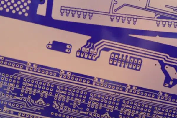
I’ve always felt that many people have their priorities backward when it comes to understanding PCBs. Everyone tends to fixate on chip models or layer counts, as if those were the only factors determining a board’s quality. In reality, what truly enables a board to operate stably for a decade or more is often the most unassuming fundamental material—specifically, the stuff known as fiberglass. You might view it as just a rigid plastic sheet, but there is a lot more to it than meets the eye.
I made this mistake myself when I first started out in hardware design, assuming that a substrate was just something that “got the job done.” Later, a batch of industrial control equipment we produced ran into major issues at a client’s site—ranging from signal interference to inexplicable reboots. After half a month of troubleshooting, we discovered the problem lay in the most fundamental area: we had used a mediocre PCB substrate to cut costs. Under the factory’s constant vibration and temperature cycling, the boards gradually deformed, causing micro-cracks to appear in the fine traces. That experience taught me that the science behind fiberglass PCBs is just as complex as designing the circuitry itself.
Speaking of glass fiber, it isn’t exactly a new invention. People began experimenting with various materials to reinforce plastic substrates as early as the mid-20th century. So, why did glass fiber ultimately emerge as the winner? I believe it comes down to its unique properties. Think about it: the material is inherently insulating—a crucial quality for circuit boards—and highly heat-resistant, capable of withstanding the high temperatures of the soldering process. Most importantly, it offers excellent mechanical strength without the conductivity or rust issues associated with metals.
However, I have to say that the quality of PCB materials marketed as “fiberglass” varies wildly these days. To cut costs, some manufacturers use loosely woven fiberglass cloth or skimp on resin formulations. Such boards might look fine initially, but various problems tend to crop up after a year or two of use. The most extreme case I’ve seen involved a consumer electronics motherboard; in less than a year, the substrate warped, causing an entire row of pins on a BGA-packaged chip to develop poor solder joints.
That’s why I pay close attention to the material datasheets provided by suppliers when making a selection. I carefully examine the glass transition temperature and the coefficient of thermal expansion—especially the Z-axis data, which is critical for multilayer boards. For key projects, I’ll even ask suppliers to send cross-section samples so I can inspect the weave density of the fiberglass cloth and the quality of the resin fill.
Of course, fiberglass PCBs aren’t a cure-all. They aren’t suitable for applications where weight is a critical concern or where flexibility and bending are required. That said, for the vast majority of electronic devices that demand stable, reliable operation—whether it’s a server motherboard in a data center rack or a control unit next to an automotive engine—a high-quality fiberglass-reinforced substrate is an investment that pays off.
I feel the industry has a bad habit of obsessing over so-called “breakthrough tech” while overlooking the potential to improve these fundamental materials.
In reality, there is still plenty of room for optimization in fiberglass PCBs—such as better balancing mechanical strength with dielectric properties or enhancing high-frequency stability. These are tangible ways to improve the quality of the final product.
Unfortunately, few manufacturers seem willing to invest R&D effort into these foundational materials; most prefer to hype up the latest chips they’re using or the flashy features they support. Ultimately, the soul of a circuit board lies not just in the code it runs or the data it processes, but in its ability to reliably support all of that across a wide range of environments.
Fiberglass—or more precisely, fiberglass-reinforced material—is that unsung yet indispensable guardian.
It may never appear on a product’s promotional page, but without it, many of the electronic devices we take for granted might never make it out of the laboratory.
I often feel that people misunderstand circuit boards. They tend to focus on the complex circuitry and components as the key elements, whereas the substrate supporting it all—such as a fiberglass-reinforced PCB—is the true, quiet hero. While it isn’t a new invention, there are solid reasons why it remains the industry standard.
Just think about the rigors a circuit board endures: from factory soldering and installation into various devices to withstanding temperature fluctuations and high-frequency signals. If the foundation isn’t solid, those precision circuits would fail in no time. Fiberglass acts much like rebar in concrete; the framework formed by curing it with resin provides essential structural support—a fact many people overlook.
I’ve seen designs where the substrate was made excessively thin in the pursuit of a slim profile; the result was a product that deformed under slight pressure and suffered from cracked solder joints. It’s a shame, really, because the issue often stems not from complex technology, but from a poor choice of basic materials. The rigidity provided by fiberglass is hard to match with other materials, ensuring the PCB maintains its shape during both manufacturing and actual use.
Let’s also consider the impact of temperature changes. Electronic devices generate heat during operation, and ambient temperatures fluctuate. Resin materials tend to expand and contract significantly when heated; if used alone for a board, dimensional stability would be compromised. Adding fiberglass changes the equation. Its low coefficient of thermal expansion effectively constrains the resin, preventing unwanted movement and ensuring minimal structural change across the board—even in high-heat environments like the reflow soldering process. This is particularly important for protecting delicate metallized through-holes, as it prevents the risk of breakage caused by uneven material expansion.
Of course, we are usually not dealing with individual glass filaments, but rather a composite structure formed by weaving these filaments into a fabric and bonding them with resin. The structure of this composite is fascinating; different weaving patterns yield different properties. For instance, a balanced weave—where warp and weft yarns interlace evenly—produces a very flat surface. This ensures excellent uniformity and dimensional stability in the final laminated PCB, qualities that are virtually essential for modern electronic products requiring high-precision component placement.
The choice of fiberglass cloth and the resin-to-fiber ratio largely determine the board’s characteristics—whether it prioritizes high-frequency signal integrity, mechanical strength, or heat resistance. Engineers essentially combine the properties of these base materials to achieve specific design goals. We sometimes focus too heavily on chip models or circuit topologies while overlooking the quality of the board itself, yet that board is a fundamental factor in determining product reliability.
Many people think selecting a PCB substrate is simply a matter of checking a datasheet. That isn’t the case. I thought so too when I first entered the field, but I later discovered the complexities hidden behind those parameters.
Take fiberglass cloth, for example. You might view it as just a layer of fabric, but the weaving pattern significantly impacts the final board’s performance. Weaves such as plain, satin, and twill directly affect the uniformity of the dielectric constant (Dk) and dissipation factor (Df), which in turn influences signal transmission consistency and loss. Differences in warp and weft yarn density can also introduce slight anisotropy—a factor that is particularly critical in millimeter-wave designs.
I have seen engineers exhaustively optimize routing designs in pursuit of signal integrity, only to neglect the fundamental issue of material selection. Sometimes, a routing scheme that took days to fine-tune yields less significant results than simply switching to a more suitable substrate. For example, moving from standard FR-4 to low-loss materials like Megtron or Tachyon can lead to immediate improvements in signal attenuation and jitter. There is a good reason why satin weave fabric is frequently used in high-speed circuits: its surface is notably smoother. For high-frequency signals, this smoothness is not merely a luxury but a necessity, as conductor surface roughness exacerbates the skin effect and increases insertion loss. Satin weave features fewer interlacing points and longer yarn floats, resulting in a smoother surface for copper foil adhesion.
Imagine driving on a bumpy, pothole-ridden road; signals traveling across a rough surface encounter similar issues. Electrical signals experience increased scattering and reflection, leading to rising-edge degradation and eye diagram closure.
However, satin weave is not suitable for every application. Its mechanical strength is relatively low, making it a less-than-ideal choice for applications involving repeated thermal cycling or a risk of bending.
If you are designing a board subject to mechanical stress—such as a motherboard for industrial control equipment—you might need to consider other weave types. For instance, in high-vibration environments, plain weave fabric offers superior dimensional stability and fatigue resistance due to its tight interlacing structure.
Plain weave offers better stability; its tighter structure resists deformation. This results in more controllable Z-axis expansion during drastic temperature fluctuations, helping to ensure the reliability of via connections.
Resin selection is also critical; the resin must be compatible with the fiber fabric. Resin systems—such as epoxy, PPO, or cyanate ester—determine not only the glass transition temperature (Tg) and thermal decomposition temperature (Td) but also, through their cured molecular structure, fiber wetting, and bonding strength, play a pivotal role in interlayer adhesion and CAF (Conductive Anodic Filament) resistance.
If a resin has poor flow characteristics and fails to fill the gaps between fibers, the resulting board is prone to delamination. This can lead to board rupture or micro-cracking during the high temperatures of subsequent assembly and soldering, creating long-term reliability risks.
I once encountered a situation where boards performed perfectly during testing but suffered inexplicable failures after mass production. It turned out the issue stemmed from a change in resin suppliers; although the specifications appeared similar, the actual performance differed significantly. Resins from different manufacturers can vary significantly in their formulations of curing agents, accelerators, and additives; even if they share the same nominal Tg (glass transition temperature) and Dk (dielectric constant) values, their processing windows, moisture absorption rates, and long-term thermal aging characteristics can differ vastly.
Therefore, material selection cannot rely solely on technical specifications; process compatibility must also be considered. Does the laminate’s curing cycle match your press parameters? Are the storage conditions and shelf life of the prepreg strictly observed? These factors all impact the final quality.
Many manufacturers are currently promoting new materials, claiming superior performance—albeit at a higher price—yet I have found that certain optimized traditional materials perform just as well while costing significantly less. For instance, through improvements in curing processes or the addition of specific fillers, some mid-Tg FR-4 materials can meet the requirements of certain high-speed consumer products that have moderate demands regarding signal loss.
It is much like buying clothes: one need not always chase the latest style; a classic design with modern refinements might actually be better suited for everyday wear. Material selection requires a comprehensive evaluation covering electrical performance, mechanical strength, thermal reliability, manufacturability, and overall cost.
The same applies to design; one should not blindly follow trends but rather clearly understand actual requirements. What is the product’s operating frequency? What are the expected service life and environmental conditions? What are the scale of mass production and the associated cost constraints?
Sometimes, what you need is not the most advanced material, but the most suitable one. Using high-end, high-speed materials for the motherboard of a consumer electronic toy would undoubtedly be a massive waste.
This principle sounds simple, yet few truly practice it, as people fear falling behind or being perceived as ignorant of new technologies. Supply chains also tend to recommend “hot” materials that offer higher profit margins or are easier to manage in terms of inventory.
In reality, those who truly understand technology know that suitability matters more than cutting-edge status, especially in engineering. The best designs often represent the optimal balance point found amidst a set of constraints.
A good design should simplify materials and processes as much as possible while still meeting performance requirements, rather than complicating simple matters. Over-specifying materials narrows the pool of qualified suppliers and increases both procurement risks and manufacturing costs.
I have witnessed far too many examples of over-engineering where costs rose while reliability actually declined—an ironic outcome, yet one that happens frequently. For example, blindly using ultra-low-loss materials that are also highly brittle can make the product more prone to stress-induced cracking during assembly. So, the next time you select a PCB substrate, don’t hesitate to ask “why”—why choose this specific weave? Why use that particular resin? You might discover that certain “industry conventions” aren’t necessarily the best fit for your specific application. Engaging in-depth with senior application engineers from material suppliers—and obtaining samples of various material combinations for actual testing—is often the foundation for making the best decision.
I’ve recently noticed an interesting phenomenon: when discussing fiberglass PCBs—specifically which type of fiberglass cloth to use—people often equate thickness directly with “strength.” There is a tendency to assume that a thicker board using a heavier-duty weave (like the 7628, a style that sounds robust just by its name) is inherently more reliable. This is actually a significant misconception.
You need to consider the speed at which signals travel across the PCB. In modern designs—especially those involving high-speed data transmission—signal integrity issues are often far more critical than mere physical sturdiness. A board might feel heavy and solid in your hand, but if internal traces suffer from severe signal reflection or excessive loss due to an uneven dielectric layer, the entire system may fail to operate reliably. I have seen designs that blindly stacked thick cloth types in pursuit of a “military-grade” sense of heft, only to see their high-frequency performance fall apart completely.
Does that mean, conversely, that one should simply aim for ultra-thin varieties? Of course not. In high-power modules or environments subject to mechanical vibration and shock—such as specific mounting locations in automotive electronics—sufficient structural support is essential. This is where thick weaves like the 7628 prove their worth: they provide a skeletal rigidity that prevents the board from warping or solder joints from cracking under harsh conditions. The key, however, is realizing that you shouldn’t deploy this “heavy tank” across the entire battlefield.
The true test of design expertise lies precisely in the art of mixing and balancing these factors. In a complex multi-layer board, the power planes and internal core layers might require 7628-style materials to ensure overall rigidity; however, the outer layers—which carry critical differential pairs and clock lines—may necessitate a switch to thinner, more uniform dielectric materials to guarantee precise, controllable impedance along the signal paths. Sometimes, it is even necessary to address areas of stress concentration through localized reinforcement or specific stack-up designs, rather than simply “beefing up” the entire board indiscriminately.
I’ve always felt that when evaluating material specifications, you can’t just look at the raw numbers; a difference in thickness of a fraction of a millimeter often reflects fundamentally different design philosophies and application scenarios. Choosing the right material for the right application allows you to balance cost-effectiveness with high performance. Conversely, if you take shortcuts or let preconceived notions dictate your choices, you end up with either a “showpiece” that fails to meet performance standards or an overpriced, clunky piece of hardware. Navigating these trade-offs is where an engineer should focus their energy—not on rote memorization of which model fits which scenario.
I’ve always felt that many people have a somewhat skewed understanding of PCBs. People love to discuss complex circuit designs or cutting-edge material technologies, yet they often overlook the fundamentals of how a pile of raw materials transforms into a functional board. It’s actually a fascinating process, especially once you’ve tried it yourself.
Take fiberglass PCBs, for example. Many assume they are simple composites—just a matter of pressing fabric and resin together. I used to think so too, until I watched the technicians at work in the factory and realized it’s far more complex. That thin fiberglass cloth feels incredibly fragile in your hands; apply a little force and the fibers start to fray. It’s hard to imagine it eventually becoming the rigid substrate that supports an entire array of electronic components.
The key lies in that transformation process. You have to ensure the resin fully permeates the gaps between every single fiber. It looks simple, but the execution requires real expertise. Factors like resin viscosity, temperature, and immersion time must be precisely controlled; otherwise, you risk incomplete impregnation—leaving air bubbles inside—or over-saturation, where excess resin runs everywhere. I’ve seen boards that looked fine initially but failed testing due to internal delamination—usually the result of a flaw in this specific step.
Then comes the actual forming stage—what is commonly known as lamination. This involves even more intricacies. You can’t just pick arbitrary numbers for temperature and pressure; they must be carefully adjusted based on the material’s specific properties. If the temperature is too high, the resin reacts prematurely and becomes brittle; too low, and the bond won’t hold. Excessive pressure can deform the internal circuitry patterns, while insufficient pressure results in a loose, poorly compacted board. And this isn’t a one-step process; it has to be done in stages: first, pre-heating to soften the materials so they conform to one another; then, increasing pressure to squeeze out any air; and finally, maintaining high heat to allow the resin to fully cure.
What stuck with me most was learning from a veteran technician how to gauge the curing level. He didn’t use instruments; he simply tapped the edge of the board with his finger and listened to the sound. A crisp, solid tone indicated a dense, uniform internal structure, whereas a dull or hollow sound meant something hadn’t been processed correctly. That kind of experiential knowledge is something you simply can’t learn from a textbook.
Many factories nowadays aim for full automation, but I still feel that certain stages require human experience and judgment. For instance, changes in ambient humidity significantly affect semi-finished products; the exact same parameters might yield a flawless board one day and a defective one the next. Machines just follow a program, but a veteran technician knows how to fine-tune the process details based on the day’s weather conditions.
Ultimately, PCB manufacturing is an art of balancing competing demands: ensuring mechanical strength so the board withstands various stresses without deforming or cracking; guaranteeing stable electrical performance and good insulation; and considering manufacturability and cost control. Focusing too heavily on optimizing just one metric often comes at the expense of others.
So, the next time you see an ordinary circuit board, give it a second thought—there’s a lot more to it than just the circuit patterns drawn on the surface!
I used to think PCB manufacturing was just a routine, step-by-step process—until I tried prototyping fiberglass PCBs myself. Many people focus primarily on circuit design, which is certainly important, but the factors that truly determine a board’s reliability and longevity lie elsewhere.
Take the curing process—the most fundamental step—as an example. It sounds simple enough: just apply heat and pressure to harden it, right? But there’s a lot of nuance involved. Even slight variations in temperature or time can lead to vastly different results. If the process is too fast, the resin won’t level out properly, potentially leaving voids; if it’s too slow, the resin might over-react, compromising performance. For instance, during the lamination of multilayer boards, the heating rate must be precisely matched to the resin system’s gelation curve. This ensures that sufficient pressure is applied when the resin viscosity is at its lowest, allowing it to expel air bubbles and fill the microscopic gaps between the glass cloth fibers. Optimizing press parameters for this process requires trial and error, tailored to the specific type and thickness of the prepreg (PP) being used.
I have seen many novices suffer significant setbacks by overlooking this step. They assume that simply purchasing high-quality base materials guarantees success, only to find their boards delaminating or blistering when exposed to even minor thermal stress. This is often caused by the rapid expansion of residual volatiles or microscopic air bubbles—trapped during lamination—when subjected to the high temperatures of subsequent reflow soldering. A classic example is a vacuum press failing to maintain sufficient vacuum levels or duration; even with expensive, low-loss materials, this can create hidden defects within the board.
True, reliable bonding strength is built incrementally throughout the manufacturing process, not achieved by simply gluing layers together at the end. Every step contributes to the final interfacial strength—from the black oxide treatment on inner layers (which creates microscopic roughness to increase bonding surface area) to maintaining a dust-free environment and controlling temperature and humidity during pre-stacking.
This brings us to the peel strength test. While the test itself appears straightforward—using an instrument to tear the copper foil from the substrate and measuring the force required—industry standards like IPC-TM-650 mandate precise methodologies (covering strip width, peel angle, and speed) to ensure results are comparable.
However, the resulting data reflects the quality of the entire lamination process, including resin flow, vacuum control, and the validity of the temperature profile. An excellent peel strength value indicates that the resin has fully wetted the copper foil’s tooth-like profile, forming a composite structure characterized by both mechanical interlocking and chemical bonding after curing.
I have a personal habit of cutting a small piece of scrap material from every prototype batch to perform a quick peel test; while not a formal laboratory procedure, it provides an intuitive sense of quality. I pay close attention to the sound of the copper foil peeling—listening for a crisp, uniform noise—and observe the state of any resin remaining on the substrate surface.
Sometimes, even if the data meets specifications, the “feel” isn’t right—such as an uneven break or powdery residue upon peeling—which makes me question the reliability of that batch of boards. Powdery residue may indicate incomplete resin curing or weak adhesion to the copper foil; in long-term hot and humid environments, this can lead to failures such as Conductive Anodic Filament (CAF) growth.
To cut costs, many manufacturers alter material specifications—such as opting for cheaper resin systems or changing the glass fabric type. For instance, replacing standard FR-4 epoxy resin with phenolic epoxy, or using a looser 106 glass weave instead of 1080, affects the material’s dielectric constant, coefficient of thermal expansion (CTE), and mechanical strength.
Lower cost doesn’t necessarily mean poor quality, but a balance must be struck. Designers need to evaluate actual product requirements: operating frequency, power density, expected environmental stress, and lifecycle costs.
High-Tg materials sound impressive due to their heat resistance, but do most consumer electronics really require such high specifications? An optimized standard material paired with a flawless manufacturing process might actually yield better overall performance and cost advantages. For example, a standard FR-4 with a Tg of 140°C—provided it has a gradual glass transition and well-controlled Z-axis CTE—can perform more stably during the brief high-heat exposure of lead-free soldering than some high-Tg materials that have narrow process windows.
I believe that judging a PCB’s quality shouldn’t rely solely on datasheet parameters; how it performs in your specific application environment is what matters most. For instance, boards used in automotive engine compartments require a focus on thermal cycling and vibration resistance, whereas high-speed digital boards prioritize dielectric constant stability and consistent dissipation factors.
Some boards pass every laboratory test perfectly but fail quickly when subjected to actual vibration or thermal cycling. This often happens because standard tests apply single stresses, whereas real-world applications involve combined stresses that can expose weaknesses at material interfaces or in through-hole copper plating.
That is why I now prioritize manufacturing transparency and process consistency over simply chasing top-tier material specifications. I look for strict incoming material inspections, robust process control points (such as measuring thickness and tolerances before and after lamination), and comprehensive traceability records. After all, even the best materials go to waste if the processing technology falls short; conversely, superb craftsmanship can turn ordinary materials into highly reliable products. That is arguably the charm of manufacturing—it is not merely about piling on materials, but about truly understanding the principles behind every step and executing them correctly.
I’ve noticed an interesting phenomenon recently: whenever people talk about the heat resistance of circuit boards, they fixate almost exclusively on the Tg value. This is actually a major misconception. Tg merely marks the transition temperature where the resin shifts from a rigid state to a softer one; while important, it isn’t the whole story. Consider that a fiberglass PCB is a composite material made of fiberglass cloth and resin; its overall performance is the result of the synergy between the two.
The resin system is indeed critical. High-Tg materials typically utilize epoxy resins with a higher number of functional groups or phenolic curing agents, and sometimes incorporate ceramic fillers. This allows the resin to better withstand high temperatures without softening easily. However, this introduces a problem: such resins often have higher viscosity and poorer flow characteristics. It’s like making a cake—if the batter is too thick, it won’t penetrate every nook and cranny effectively. During the lamination of multilayer boards, if the resin fails to properly wet and fill the gaps within and between the fiberglass cloth layers, it can leave behind voids or resin-starved areas—which pose a genuine reliability risk.
Therefore, simply placing an order based on a high Tg value isn’t enough; you have to consider the compatibility of the entire system. For instance, if you choose a high-Tg prepreg, it is best paired with a fiberglass cloth of moderate weave density, such as the 2116 style. Cloth that is too loose may fail to retain the flowing resin, while cloth that is too tight might hinder uniform resin filling. Finding the right balance is key. Requirements become even more stringent for boards featuring large areas of thick copper or those subjected to extreme thermal shock. In such cases, one might even consider specially treated fiberglass materials—such as “spread-glass” (open-weave) or NE-glass cloth—to reduce the Coefficient of Thermal Expansion (CTE) along the Z-axis. This helps prevent fatigue fractures in the copper rings on the via walls caused by repeated thermal expansion and contraction. Ultimately, when it comes to FR-grade laminates—whether standard FR or high-reliability variants—the core challenge lies in balancing reliability, manufacturability, and cost. Skimping on a few dollars by using materials with inadequate Tg values or poor compatibility significantly increases the risk of failure during reflow soldering or prolonged exposure to high outdoor temperatures. The resulting costs—covering repairs, replacements, and potential damage to brand reputation—can far outweigh the initial savings. Material selection is an art requiring comprehensive judgment, not merely a matter of checking boxes against a datasheet.
I’ve recently been working with a high-frequency board and discovered an interesting phenomenon. I used to view fiberglass PCBs as basic, run-of-the-mill materials, but I’ve come to realize there is a lot more nuance involved. Once signal frequencies exceed a few gigahertz, a board that appears uniform is actually anything but.
You might be surprised to learn that the fine glass fibers inside the board are actually woven together. This creates a problem: the path beneath a signal trace might alternate between areas rich in glass fiber and areas rich in resin. These two materials have vastly different dielectric properties. I once compared measurements and found that identical traces yielded noticeably different propagation delays depending on their location—a disaster in high-frequency environments. For instance, at 10 GHz, this non-uniformity can cause a timing skew of several picoseconds between adjacent signal channels; this is enough to disrupt the synchronization of high-speed parallel buses and trigger severe inter-symbol interference.
I’ve seen people route traces at odd angles in an attempt to circumvent this issue. They assume that routing diagonally allows them to bypass the pattern of the fiberglass weave, but that’s actually a clumsy approach. The root cause is the uneven distribution of material properties; simply adjusting the routing direction doesn’t solve the fundamental problem. In fact, diagonal routing can increase trace length, introduce extra loss and reflection, and waste valuable routing space.
In my view, rather than racking your brain trying to work around the problem later in the design process, it is far better to select the right material from the start. Some manufacturers now offer modified fiberglass boards specifically designed for high-frequency applications; these utilize special processing techniques to ensure a more uniform fiber distribution. While they may cost a bit more, they save a great deal of trouble during the debugging phase. For instance, using flat-weave fiberglass or randomly oriented glass fiber mats can significantly reduce local fluctuations in the dielectric constant (Dk), keeping the variation within 3%—a critical factor for millimeter-wave circuits.
I recall helping a friend troubleshoot a project where the boards performed perfectly in the lab but encountered inexplicable signal integrity issues during mass production; it turned out to be caused by subtle differences in the weave density of the fiberglass cloth across different batches. Such issues are impossible to foresee during the design phase and rely entirely on material consistency. Even with the same supplier, different production batches of fiberglass cloth can exhibit slight variations in warp and weft yarn tension or resin curing levels, all of which ultimately affect the batch-to-batch stability of dielectric performance.
Another point often overlooked is that the Dk value is not static; it fluctuates with frequency. Data measured at low frequencies may not apply at high frequencies. Therefore, when selecting materials, one shouldn’t rely solely on the manufacturer’s nominal values; it is best to obtain test data for the specific frequency range of the application. For example, a material with a Dk of 4.0 at 1 GHz might drop to around 3.8 at 24 GHz; this frequency dispersion characteristic directly impacts transmission line impedance control and phase consistency.
When working on high-frequency designs now, I always engage in in-depth discussions with material suppliers to understand their manufacturing processes and quality control standards. Some lesser-known manufacturers actually offer materials that perform better in specific frequency bands. You need to conduct your own verification testing rather than relying blindly on promotional literature. I usually request full-spectrum test reports detailing the complex dielectric constant (including Dk and Df) across various frequencies, and I may even verify performance in critical bands myself using methods like the resonant cavity or transmission line technique.
Ultimately, the “fiber-weave effect” serves as a reminder that hardware design requires an understanding of materials and manufacturing processes, not just circuit schematics. Sometimes, the issue isn’t the sophistication of your design, but whether the base materials are suitable for the specific application. For instance, the requirements for material consistency in 77 GHz automotive radar modules are far more stringent than those for standard 2.4 GHz Wi-Fi modules; the former often necessitate the use of ultra-low-loss PTFE-based substrates. I find the most interesting aspect of this industry to be the constant search for the optimal balance between performance and cost. You might be aware of a superior solution, but you have to consider whether the client will accept the price point. This is where an engineer’s experience comes into play—knowing when standard materials suffice and when high-end materials are essential. For instance, with consumer electronics, one might accept a slight trade-off in performance margins to keep costs down; however, for aerospace or medical equipment, material consistency and reliability must take precedence.
I always get excited when I encounter technical details like this because it’s an opportunity to learn something new. That’s the nature of hardware design: there are always fresh challenges waiting to be solved. From materials science and electromagnetic theory to manufacturing processes, a deep understanding of every aspect helps us find optimal design paths amidst complex constraints.
I was recently discussing material selection with some friends in the PCB industry. They often get hung up on the specific figures listed in technical datasheets. Honestly, I think we often overcomplicate things. Take fiberglass PCBs, for instance: many people fixate on the dielectric constant (Dk) right away, assuming lower is better and eager to switch to the most expensive substrate available.
But reality is often different. I recall a project where we used an imported material touted for its exceptionally low Dk, only to find the impedance control on the finished boards was a disaster. We later discovered an issue with the fiber-resin match; the uneven fiber distribution within the material caused significant local fluctuations in dielectric properties.
This reminds me of my days in the university lab. We used very ordinary materials back then, but our professors taught us how to compensate for material limitations through layout and routing strategies. For example, you could deliberately adjust the angle of critical traces to avoid areas where fiber bundles were densely packed. It might sound like a low-tech approach, but it was highly effective and cost nothing.
Nowadays, many manufacturers love to hype up the fine fibers or unique weave patterns used in their new materials. Concepts like satin weaves and low-Dk resins are certainly appealing. However, I believe the key lies in the overall synergy of the components. Even the best fibers won’t yield a good board if paired with the wrong resin.
I once visited a small PCB shop; their equipment wasn’t state-of-the-art, but the veteran technicians were incredibly experienced. They used standard fiberglass cloth but adjusted process parameters to ensure exceptionally uniform resin impregnation. The resulting boards actually performed more consistently than those made by some major manufacturers using high-end materials.
That’s why I take a more pragmatic approach to material selection now. Expensive materials aren’t automatically superior, nor does an impressive datasheet guarantee success. You have to consider how the entire design chain works together—holistically evaluating materials, manufacturing processes, and design.
Sometimes, opting for standard materials while putting extra effort into design and process optimization yields better results. Of course, this requires engineers to truly understand material properties, rather than just relying on datasheets.
I’ve seen too many people blindly chase new materials and processes, only to waste money without solving the underlying problems. In reality, many traditional materials can fully meet most requirements if applied correctly. Ultimately, when it comes to engineering, you can’t rely solely on specifications on paper; you have to consider real-world application scenarios. Every project has unique requirements, and no single material is a universal solution; the key is finding the one that best fits the specific needs at hand.
Many people assume that since a circuit board is tucked away inside a housing—out of sight—the choice of material doesn’t really matter. I used to think the same way. That changed when I was in charge of an outdoor communication equipment project. The prototype passed all tests perfectly, but after just a few months of field deployment on a tower, we encountered inexplicable intermittent signal issues. Upon disassembly, we found the culprit: the standard PCB had developed hairline cracks at the base of the pads for several large connectors, caused by prolonged exposure to the elements and daily temperature fluctuations. That realization was a real wake-up call.
That experience completely changed my perspective. In the industrial sector, a circuit board is far more than just a carrier for circuitry; it acts as the structural backbone of the entire device, capable of withstanding harsh environments. Consider machines on automated production lines that vibrate and operate 24/7, or the environment under a car hood—where temperatures can soar high enough to cook an egg in summer and plummet to freezing in winter. Standard paper-based or composite substrates fail quickly in such conditions. They might warp due to moisture or suffer from delamination—where the layers separate—caused by thermal expansion and contraction.
This is where choosing a fiberglass-reinforced PCB becomes crucial. The rigidity—or structural integrity—offered by this material is unmatched by standard alternatives. It ensures the board maintains a stable physical shape, which is vital for boards carrying large, heavy connectors or power components. If the board is flimsy, the force from plugging and unplugging connectors or from equipment vibration is transferred directly to the fragile solder joints. Over time, fatigue and cracking at these joints become inevitable. A robust fiberglass PCB, however, effectively distributes these stresses, protecting those critical electrical connection points. I have seen far too many engineers focus all their energy on the “brain” of the system—chip selection and circuit design—while neglecting the health of its “skeleton.” They might choose cheaper board materials to save a few dollars, only to pay a much higher price during reliability testing or actual deployment. Take, for instance, a controller installed next to a large motor: if the motherboard warps or bends due to constant vibration, the BGA-packaged chips are the first to suffer; if even a few of the densely packed solder balls underneath crack, the system fails. Such issues are insidious and notoriously difficult to troubleshoot.
That is why I always emphasize one point when discussing designs with my team: before deciding on the board’s “bones and sinews,” you must first understand the “environment” it will inhabit. For the vast majority of industrial applications facing challenges like vibration, temperature fluctuations, and humidity, selecting a reliable fiberglass PCB substrate from the start isn’t a waste of money—it’s a necessary investment that saves you from costly, hard-to-fix headaches down the line. It’s just like laying the foundation for a house; you can’t focus solely on the beauty of the design above ground—you have to ensure the underground foundation is solid enough to withstand the elements.
I recently chatted with some friends in the PCB industry and noticed an interesting trend: whenever people talk about AI hardware, they focus on chip computing power and power consumption. Yet, the underlying foundation supporting these complex systems is often overlooked—those seemingly ordinary circuit board materials are actually the key.
Many people may not realize that high-performance PCBs rarely use traditional materials these days. I remember when, just a few years ago, the debate was whether standard FR4 material would suffice. The situation has changed completely now, especially for equipment like AI servers. I’ve seen design teams forced to re-evaluate their entire substrate material strategy to minimize signal loss. They discovered that conventional epoxy resin systems caused significant dielectric loss during high-speed signal transmission.
This reminds me of a case I encountered earlier: an AI accelerator card developed by a certain company kept running into signal integrity issues during initial testing. After checking the chip packaging and routing design without finding any faults, they finally discovered that the PCB substrate’s dielectric constant was too high, causing signal attenuation. The problem was only resolved after switching to specialized fiberglass cloth reinforcement materials. This example illustrates a key point: sometimes, it is the most fundamental components where things are most likely to go wrong.
Demand for high-performance PCBs is indeed growing rapidly in the market. I’ve noticed many manufacturers developing new fiberglass cloth formulations to meet the needs of various applications. For instance, some manufacturers have developed laminates with special weave structures specifically for high-frequency applications. These materials effectively control the dielectric constant and dissipation factor while maintaining mechanical strength. While the average consumer might not pay much attention to these technical details, they are absolutely critical to engineers.
A supplier I know mentioned that they are receiving an increasing number of inquiries for materials with specialized specifications. In the past, customers might simply ask, “Do you have FR4 boards?” Now, they ask for specific details like the dielectric constant, glass transition temperature, and whether the coefficient of thermal expansion meets their requirements. This indicates that the industry’s demands regarding material performance are becoming increasingly precise.
Another noteworthy trend is the localization of the supply chain. High-end PCB materials used to rely heavily on imports, but domestic manufacturers are gradually upgrading their technical capabilities. I once visited the production line of a local fiberglass cloth manufacturer and discovered they had already begun mass-producing mid-to-high-end products.
That said, the cost pressure associated with material upgrades is significant. High-performance fiberglass cloth reinforcement materials cost considerably more than standard versions, posing a real challenge for many small and medium-sized equipment manufacturers.
I believe this sector will continue to evolve over the coming years. As more AI applications are deployed, the demand for hardware performance will only rise, and suppliers capable of providing stable, reliable, high-performance materials will become increasingly valued. After all, even the most powerful chip needs a reliable circuit board to support its computing capabilities.
Many people view the PCB merely as a board that holds components, but it is far more complex than that. Through my work on various projects, I’ve found that what truly determines whether a board can withstand rigorous conditions isn’t usually the circuitry on the surface, but the layer of fiberglass cloth embedded within the resin. It acts much like the steel framework of a building—invisible to the naked eye, yet if the wrong type is chosen or the quality is substandard, the integrity of the entire structure is at risk.
I have seen cases where standard-grade fiberglass cloth was chosen to cut costs, and the results were far from ideal. Take, for instance, a team developing outdoor surveillance equipment: the PCBs they initially used suffered from minute deformation in environments with significant temperature fluctuations, leading to cracked solder joints; the issue was only resolved after switching to a higher-specification fiberglass cloth substrate. This made me realize that we often focus too heavily on component brands and specifications while overlooking the reliability of the substrate itself.
The sheer variety of fiberglass cloth specifications on the market today is dizzying—ranging from common models to low-loss materials optimized for high-frequency signals—but this abundance brings its own challenges. I’ve noticed that engineers often fall into one of two extremes when making a selection: either they blindly chase top-tier materials, resulting in unnecessary waste, or they remain overly conservative, sticking to outdated solutions that fail to meet the performance requirements of new products.
In reality, standard fiberglass cloth is sufficient for most consumer electronics; there is no need to blindly upgrade just to chase better specs. However, for equipment operating in harsh environments or requiring exceptional signal integrity—such as RF modules in base stations or automotive control units—you must carefully consider the substrate material’s properties. This is where low-dielectric fiberglass cloth proves its value by effectively reducing signal transmission loss—a critical factor for high-frequency circuits.
My personal view is that the choice of fiberglass cloth should be based on the product’s actual application scenario rather than just the datasheet. Sometimes, slightly raising the substrate standard can significantly boost the overall device’s reliability—a far more cost-effective approach than trying to fix problems after the fact. Of course, this requires a solid understanding of manufacturing processes and material properties; you cannot simply leave the decision entirely to the supplier.
Another often-overlooked factor is supply chain stability. A good fiberglass cloth supplier provides not only qualified products but also batch-to-batch consistency—something crucial for mass production. I once encountered a situation where changing the substrate supplier caused the yield rate for an entire batch of PCBs to drop, and it took a long time to identify the root cause. Consequently, I now prefer working with material suppliers who have a proven track record of long-term cooperation, even if the price is slightly higher.
Ultimately, while the fiberglass cloth in a PCB may seem inconspicuous, it quietly underpins the operation of the entire electronic device. When you open up an old device that has been in use for years and find the circuit board as sturdy as ever, high-quality fiberglass cloth likely played a key role in that durability.
BMS reliability isn’t decided by algorithms — it’s decided by the PCB
Beamforming performance depends on phase coherence across every antenna element — and
A relay control board that works perfectly in the lab can fail
- Experto en producción de lotes pequeños y medianos
- Fabricación de placas de circuito impreso de alta precisión y montaje automatizado
- Socio fiable para proyectos electrónicos OEM/ODM
Horario comercial: (de lunes a sábado) De 9:00 a 18:30