
Battery Monitoring System PCB: Why the Hardware Foundation Determines Everything Else
BMS reliability isn’t decided by algorithms — it’s decided by the PCB
Whenever I come across online discussions debating whether or not to attempt rework following a BGA assembly failure, I can’t help but chuckle. Many people oversimplify the matter. They seem to think, “Isn’t it just a matter of blowing the chip off and soldering it back on? How much could that possibly cost?” This mindset, in itself, is quite dangerous.
I have seen far too many factories—in an attempt to save on the immediate, so-called “scrap costs”—stubbornly persist in tinkering with boards that have already malfunctioned. The result? A board that initially suffered from just a single faulty solder joint ends up completely ruined after enduring multiple rounds of hot-air rework. Not only is a significant amount of human effort and time wasted, but the board often still has to be scrapped in the end anyway. Worse yet, a latent defect within a single chip could potentially trigger cascading failures across an entire product batch over the coming years—a financial loss that far exceeds the cost of a single PCB.
When the topic of costs arises, most people’s immediate reaction is to think of equipment expenses, labor wages, and material costs. However, these represent merely the tip of the iceberg; what truly causes headaches are the invisible costs. Take opportunity costs, for instance: halting a production line to troubleshoot a complex multi-layer board inevitably leads to delays in fulfilling other orders—how does one even begin to quantify that loss? Furthermore, technical personnel’s energy is repeatedly consumed by these inefficient remedial tasks instead of being directed toward optimizing front-end processes to prevent future recurrences. This kind of chronic internal drain on resources is, ultimately, the most expensive cost of all. In my own experience—particularly regarding high-density BGA packages used in critical equipment—rather than agonizing repeatedly over whether a faulty component can be salvaged, it is far better to establish a clear “red line” right from the start. For instance, you might limit yourself to a single attempt at professional rework; if that fails, you cut your losses decisively and redirect your resources toward a root-cause analysis. Determine whether the issue stems from solder paste printing or an improperly configured reflow temperature profile. Plugging the leak at the source is vastly more effective—and far more cost-efficient—than attempting to patch things up after the fact.
Of course, this isn’t to say that a one-size-fits-all approach applies to every situation. For simpler, low-pin-count BGAs—or during the prototyping phase where rework is necessary to validate a design—such interventions are entirely understandable. However, this is contingent upon a critical prerequisite: you must have a crystal-clear understanding of exactly what you are doing. You must ensure your equipment is sufficiently professional-grade and that the operators possess adequate experience; otherwise, you are merely gambling on luck—and uncertainty is the manufacturing industry’s greatest nemesis.
Ultimately, quality control in BGA assembly is a complex systems engineering challenge. You cannot realistically expect to guarantee reliability by relying on “miraculous cures” at the very end of the process chain. The true effort must be invested upstream: in Design for Manufacturability (DFM) reviews, in rigorous incoming material inspections, and in the precise control of every single stage along the production line. Eliminating problems while they are still in their infancy is infinitely wiser—and more economical—than scrambling to “repair” them after they have already manifested. This is the mindset that should govern high-end electronics manufacturing.
Many people assume that if a problem arises during BGA assembly, a simple rework will resolve it—as if the process were no different from merely swapping out a standard component. I, too, held this belief in the past, until I personally handled a batch of boards that had undergone rework; that experience completely changed my perspective. It felt akin to applying a screen protector to a smartphone with a shattered display: while the surface might look functional, the underlying damage is already irreversible. Every instance of heating, desoldering, and resoldering a BGA package essentially amounts to mortgaging the circuit board’s future integrity. Heat is not magic; the physical transformations it induces are tangible and real.
I have witnessed factories—in a desperate rush to meet production deadlines—subject the BGAs on a single board to repeated cycles of rework and manipulation. The result? Those boards would pass initial functional testing with flying colors—some even clearing final factory inspection. Yet, once they reached the customer’s hands and entered daily operation for a few months, a host of bizarre and inexplicable malfunctions would begin to surface: intermittent solder joints, signal instability, or even chips that simply “went on strike.” This is not a matter of bad luck; it is the inevitable consequence of a flawed process. The crux of the issue lies in the fact that we too easily equate “functional restoration” with “restoration of health.” Once a BGA package has undergone high-temperature reflow soldering, the microstructure of its internal solder joints has already formed a stable bond. When you reheat it to a molten state—typically to repair a specific fault—you are effectively completely disrupting and then reconstituting that previously stabilized structure. This process accelerates the growth of intermetallic compounds within the solder alloy, rendering the solder joints more brittle and less resistant to fatigue than they were originally. It is akin to repeatedly bending a metal wire; eventually, it will fracture at its weakest point. Specifically, under repeated thermal cycling, the grain structure of the tin-silver-copper alloy within the solder joints coarsens and develops micro-cracks; these microscopic defects are highly prone to propagating when subjected to subsequent mechanical stress. Furthermore, repeated heating exacerbates Z-axis expansion in the PCB substrate material, potentially causing the internal copper foil layers to delaminate from the resin—a phenomenon that can trigger even more insidious interconnection failures.
Therefore, when discussing the “lifespan” of a BGA, one absolutely cannot judge it solely by whether it powers up and functions in the immediate moment. True longevity is defined by the component’s ability to maintain a stable connection over the coming years, even after enduring temperature fluctuations and mechanical vibrations. A single rework operation can significantly compromise its capacity to withstand this kind of routine wear and tear.
This also brings to light a very real decision-making dilemma: When faced with a defective—and often expensive—motherboard, should one invest the time and cost to rework it, or simply scrap it? Many people instinctively opt for the former, under the impression that they are “saving money.” However, we often fail to properly calculate the other side of the ledger: What are the potential costs—in terms of customer complaints, warranty claims, and even damage to brand reputation—if that reworked board fails prematurely? For instance, if an industrial controller operating on a production line suffers an unexpected shutdown due to a previously reworked BGA, the resulting production losses could easily amount to tens of times the cost of a brand-new motherboard. Such latent risks are frequently underestimated or entirely overlooked during the decision-making process.
I have gradually formed a somewhat steadfast conviction: For critical, core BGA components—particularly those deployed in equipment requiring long-term operational stability (such as industrial control systems or medical devices)—if a fault arises during the initial assembly phase, one must exercise extreme caution and rigor when evaluating the feasibility of attempting a rework. When conducting an assessment, one must look beyond mere process capability; it is equally critical to analyze the thermomechanical stress loads that a specific solder joint will be required to withstand throughout the product’s entire lifecycle. Indeed, certain high-reliability standards explicitly prohibit secondary reflow operations for critical BGA components.
At times, the psychological gratification and short-term financial savings derived from “resurrecting” a faulty board pale in comparison to the prudence of simply accepting the loss and starting afresh with a brand-new unit. The latter approach offers a definitive and uncompromised expectation regarding the product’s full lifecycle. This necessitates that engineers and managers suppress the instinctive urge to “save the hardware,” opting instead to make dispassionate, calculated decisions based on system-level reliability and total lifecycle costs.
Ultimately, this issue boils down to the depth of our understanding of the term “repair.” In the realm of electronics manufacturing—particularly when dealing with intricate structures like BGAs—a “repair” rarely equates to turning back the clock to restore the component to its original, pristine state; rather, it is often more akin to a compromise—a mere patch. Only by acknowledging the potential ramifications of such compromises on long-term reliability can we make truly responsible decisions. This realization also serves as a catalyst for the industry to place greater emphasis on “First Pass Yield” and to develop more sophisticated non-destructive inspection technologies—such as 3D X-ray and acoustic microscopy—thereby enabling the timely detection of defects during the assembly phase and fundamentally reducing the reliance on rework operations.
Whenever I encounter discussions regarding the reliability of BGA assemblies, I feel compelled to chime in with a few observations. Many people harbor a misconception that these components are inherently fragile and incapable of withstanding any form of stress or manipulation.
I have witnessed far too many engineers whose immediate instinct, upon encountering a problem, is to rush into BGA rework—operating under the assumption that simply re-balling the component will magically resolve all their troubles. This mindset is inherently hazardous, as the root cause of the problem often lies entirely elsewhere—not within the solder balls themselves.
What truly exasperates me is the practice of subjecting the same specific location on a board to repeated rework attempts. Some individuals seem to believe that, provided the procedure is executed with sufficient skill, a component can be repaired an infinite number of times—a notion that borders on pure fantasy.
Each successive heating cycle inflicts cumulative damage upon the PCB substrate material. Although this damage remains invisible to the naked eye, it can severely compromise the long-term stability of the circuit board. For instance, common FR-4 substrate material—after enduring multiple thermal cycles that exceed its Glass Transition Temperature (Tg value)—will experience a gradual degradation in both its mechanical strength and dielectric properties. This degradation can lead to internal circuit traces fracturing or the formation of micro-cracks—latent defects that may not necessarily manifest themselves immediately during the functional testing phase. When it comes to solder joint quality, I feel that many factories today rely too heavily on their equipment, operating under the assumption that simply purchasing the most expensive machinery guarantees flawless results.
In reality, the operator’s experience and judgment are the critical factors that determine success or failure. I have witnessed far too many instances where entire batches of products were scrapped due to a blind faith in automation. For instance, Automated Optical Inspection (AOI) equipment—due to improper programming or lighting interference—might erroneously flag a perfectly sound, well-formed solder joint as having a void, or vice versa. In such cases, an experienced technician is required to make the final determination, often by cross-referencing with X-ray imaging or cross-sectional analysis.
As for those so-called industry standards—such as the rule limiting rework attempts to a maximum of three—I view them merely as reference figures.
What truly matters is your ability to identify the root cause of a specific failure. If the issue stems from internal PCB delamination or a defect within the chip itself, then no matter how much you tinker with that particular solder joint, your efforts will be entirely in vain.
I recall a specific case involving a recurring failure: we replaced the BGA component three times, yet the problem persisted. We eventually discovered that the issue lay in the PCB’s original design—specifically, a minuscule impedance mismatch.
This experience taught me a valuable lesson: sometimes, the most complex solutions are not the most effective ones; in fact, they can often lead you astray.
Many manufacturers today are actively promoting lead-free soldering processes, touting them as being more environmentally friendly and reliable. However, I have found that lead-free components actually possess a much narrower soldering process window and impose far stricter requirements on temperature control. Take the commonly used SAC305 alloy, for example: while its melting point is approximately 217°C, the ideal peak temperature during reflow soldering must be maintained within a range of 235°C to 245°C. This process window—spanning a mere 30°C—is significantly more demanding than that of traditional lead-based solders, requiring extremely precise control over preheating, ramp-up rates, and cooling rates.
Consequently, if your equipment lacks sufficient precision or your operators lack adequate experience, you run a high risk of generating defects such as “cold joints” or “dry joints”—flaws that may very well go undetected during initial functional testing.
Regarding the selection of rework equipment, I believe there is no need to blindly chase after the latest and most expensive technologies; the key is to choose tools that are best suited to your specific operational needs.
Some simple repair tasks can be accomplished using a traditional hot-air gun combined with skilled technique, whereas more complex repairs involving multi-layer PCBs may necessitate the use of infrared or laser-based heating systems. For instance, when dealing with complex HDI boards featuring numerous vias or embedded components at the base, a laser rework system—thanks to its precise, localized heating capabilities—can effectively minimize thermal impact on surrounding sensitive areas.
However, regardless of the equipment used, one crucial point must always be kept in mind: every heating cycle induces thermal stress across the entire circuit board—stress that is cumulative.
Therefore, my recommendation is to conduct a comprehensive failure analysis before deciding whether to proceed with BGA rework. You must pinpoint the root cause of the problem rather than rushing to simply patch up a detached solder ball the moment you spot it. This analysis might involve using thermal imagers to locate short circuits, utilizing boundary scan testing to verify logic failures, or performing dye penetration tests to trace the propagation paths of cracks.
Quite often, replacing the entire module or redesigning a specific section of the circuit proves to be the more economical and reliable option. While this may sound like a more cumbersome approach, it actually saves you a significant amount of time and avoids substantial future maintenance costs.
The longer I spend in this industry, the more I realize that sometimes, “slow is fast.” Those methods that appear to be shortcuts often end up creating far greater headaches for you down the road.
I’ve witnessed plenty of trouble on the production line caused by BGA warping—it’s a truly maddening experience. Just imagine: a board finally makes it to the final assembly stage, only for the component package to deform under heat; consequently, some solder joints are pulled apart while others are crushed together. Often, the problem doesn’t manifest immediately; the board might barely pass testing, only to fail once it reaches the customer—at which point the cost of rework becomes prohibitively high.
Many people believe that resolving this issue requires nothing more than more precise equipment or more complex process parameters. However, I would argue that the true key lies in understanding how the materials themselves “breathe.” Different substrate materials, chip dimensions, and even ambient humidity levels cause components to expand and contract to varying degrees during heating and cooling cycles. Sometimes you might spend ages tweaking the temperature profile with little to no visible improvement; this is likely because you’ve overlooked the non-uniform distribution of internal stress within the board. I recall a specific case where an engineer placed the boards in a constant-temperature and humidity chamber for several hours of pre-conditioning prior to BGA assembly and reflow soldering; the resulting warping was significantly reduced—a solution far simpler and more effective than merely adjusting the furnace temperature profile. For instance, with highly hygroscopic materials like FR-4, pre-treatment effectively balances internal moisture levels, thereby reducing the additional stress generated by the rapid vaporization of moisture at the peak temperatures of the reflow soldering process. Essentially, this method allows the material to undergo a portion of its deformation and release internal stresses in a controlled environment beforehand—a process analogous to “aging treatment” in metalworking.
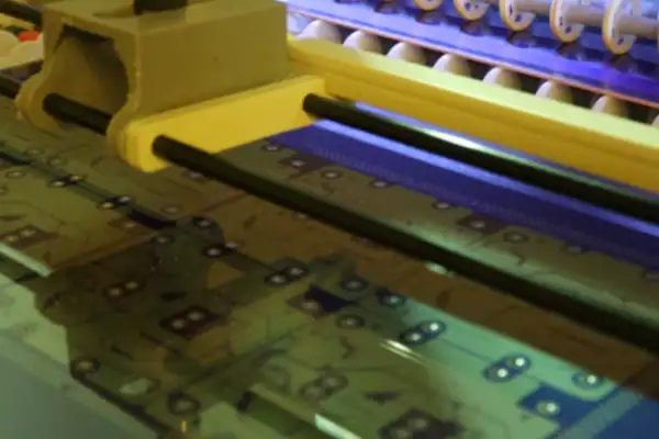
Speaking of rework, the most vexing challenge is often not the removal of the defective BGA itself, but rather ensuring that the surrounding components remain unaffected. This is particularly critical today, as many PCBs feature dense, double-sided component placement; when you apply heat to one side, the tiny components on the reverse side may already be reaching their thermal limits. I have experimented with various thermal shielding materials—ranging from standard aluminum foil to custom-fabricated silicone pads—and the results have varied significantly. While some materials effectively block heat, they may also obstruct the airflow of the hot-air rework station, leading to localized temperature inconsistencies that, ironically, induce new deformations. I eventually realized that instead of chasing perfect thermal isolation, it is far more effective to incorporate “rework access” considerations during the design phase—for instance, by leaving a small clearance zone around potentially problematic BGAs to facilitate easy manipulation. Specifically, during the PCB layout stage, one can avoid placing components that are highly heat-sensitive or possess significant height in the immediate vicinity of critical BGA devices, thereby creating the necessary physical clearance for the placement of rework tool heads or thermal shields. This mindset—known as Design for Rework (DFR)—effectively mitigates the difficulty and risks associated with subsequent rework operations right at the source.
Another frequently overlooked aspect is the post-rework cleaning process. Many people assume that simply dragging a desoldering wick across the area to remove excess solder is sufficient; however, if flux residues are not thoroughly removed, they can gradually corrode the solder pads or even seep into the substrate material itself. My standard practice is to follow up the desoldering wick application with a meticulous wipe-down using a cotton swab dipped in a specialized cleaning agent. Although this adds a few extra minutes to the process, it effectively prevents a host of potential reliability issues down the line. This is especially critical for processes utilizing “no-clean” fluxes, where one is more prone to letting one’s guard down; yet, under long-term humid and high-temperature conditions, these residues can still trigger electrochemical migration, leading to a degradation of insulation resistance or even short circuits. Consequently, for products with stringent reliability requirements, a localized, deep-cleaning procedure following any rework operation is an absolutely indispensable step.
In reality, when discussing BGA assembly processes, many factories today rely too heavily on data and equipment specifications, operating under the misconception that simply purchasing more expensive machinery will resolve all their issues. However, I believe the truly critical factor is whether the operators can grasp the underlying physical principles behind every step—for instance, understanding why a specific area requires slower heating while another demands rapid cooling. At times, a seasoned veteran can assess the condition of a circuit board purely by touch—a capability far superior to that of novices who merely stare at screen parameters. This intuition, honed through years of accumulated experience, is often something that machines simply cannot replicate. For example, by observing the changes in luster and fluidity of the solder as it melts, such an expert can roughly discern minute discrepancies between the actual furnace temperature and its setpoint, or even anticipate that certain specific batches of circuit boards may require a distinct preheating strategy.
Of course, I am not suggesting that equipment is unimportant; high-precision alignment systems and controllable heating platforms can indeed significantly boost success rates. However, if you pin all your hopes on the machinery while neglecting the human element, you will likely end up overwhelmed by various unforeseen complications. After all, the actual conditions encountered on a production line change constantly every day; no matter how intelligent a machine is, it still requires human insight and adjustment. For instance, when there are subtle variations in incoming material batches, or when ambient temperature and humidity fluctuate drastically, the equipment’s preset programs may fail to adapt automatically. At such times, experienced engineers or technicians are needed to quickly assess the situation based on observed phenomena, fine-tune process parameters, or implement temporary countermeasures. This capacity for flexible, adaptive response is a crucial “soft skill”—a key intangible asset—for ensuring the stable operation of a production line.
I have seen far too many people oversimplify the process of BGA assembly rework. They often operate under the assumption that if a board fails, the only responsible course of action is to rush to salvage it. In reality, the exact opposite is often true.
A friend of mine worked for a while at a company that manufactures industrial control equipment. A batch of motherboards on their production line developed a defect, and a portion of them needed to be addressed. The management’s initial reaction was to find someone to evaluate whether BGA rework could be performed to mitigate their financial losses.
However, the subsequent assessment revealed that repairing these motherboards would not only require a massive investment of manpower and resources but also entail significant latent risks—even if the repairs were technically successful, the thermal stress involved could shorten the boards’ subsequent service life or even introduce new points of failure.
More critically, the various chemical solvents and waste materials—such as discarded solder balls—generated during the repair process are extremely difficult and costly to dispose of properly. And that doesn’t even account for the materials that would be completely scrapped if the repair attempts failed!
Ultimately, they decided to simply scrap the defective batch of motherboards and purchase new components for fresh production and assembly runs. Although this appeared to result in a financial loss on paper, it actually saved time, reduced risk, and eliminated the environmental compliance pressures associated with waste disposal.
Therefore, I believe that when faced with similar issues, we should not fixate solely on the technical question of “Can it be repaired?” but rather focus on the far more practical question: “Is it worth repairing?” Sometimes, opting to replace a component outright rather than attempting to repair it proves to be the wiser choice—a strategy that not only guarantees product quality but also minimizes unnecessary resource waste and sidesteps the various complications associated with waste disposal.
Of course, this does not imply that repair efforts should be abandoned in every scenario; for components of exceptionally high value—or critical parts that are genuinely difficult to replace—professional BGA repair remains a necessary and viable option.
Nevertheless, we must always prioritize environmental protection and social responsibility in our decision-making. After all, we all inhabit this planet, and surely, each of us bears an obligation to contribute our share toward its preservation, doesn’t we?
Many enterprises today are striving to embrace the so-called “circular economy,” hoping to curb the generation of electronic waste through repair and reuse. While the underlying concept is laudable, its practical implementation often overlooks the new environmental issues that the repair process itself might inadvertently create.
For instance, the chemical solvents used to clean circuit boards can contaminate soil and water sources if not disposed of properly; discarded solder balls, if carelessly discarded, can also inflict negative impacts on the environment; and even the energy consumed during heating processes constitutes a form of resource waste in its own right.
Therefore, I believe that rather than blindly chasing a “zero-waste” ideal, we should approach this issue with greater rationality. The more effective strategy is to minimize unnecessary repair activities—while strictly upholding product quality and safety standards—thereby reducing the likelihood of waste generation at its very source.
After all, the most effective form of environmental protection is not reactive cleanup, but proactive prevention—wouldn’t you agree?
I often feel that many people today tend to overcomplicate the subject of BGA rework. The moment the topic arises, the conversation invariably veers toward sophisticated concepts—fully automated systems, AI-driven thermal profile analysis, and the like. In reality, however, the issues involved are often far less mysterious than they appear. I have encountered numerous engineers who, the moment they encounter a BGA soldering defect, rush to procure the most expensive equipment available for the rework—as if the sheer sophistication of the machinery guarantees a successful outcome. Yet, the reality is that many soldering defects could have been avoided during the initial assembly phase, or could be resolved using far simpler methods.
What truly gives me a headache is that mindset of “over-engineering.” Everyone seems to operate under the default assumption that BGA rework must inherently be a high-tech, high-precision undertaking—thereby overlooking the fundamental principles of the underlying manufacturing processes. Take solder materials, for instance: the market is currently flooded with a dizzying array of low-temperature, lead-free formulations, each touted with extravagant, hyperbolic claims. However, I’ve noticed that many manufacturing facilities switch to new solder alloys yet continue to rely on their old heating profiles and pressure parameters. The result is that the problems encountered after rework often outnumber the original defects. It’s akin to buying a brand-new pair of running shoes but continuing to run with a competitive walking gait—it would be a miracle if you felt comfortable doing so.
In my view, the core of BGA assembly and rework lies in understanding and controlling thermal energy. It isn’t about mysterious AI algorithms, but rather the tangible accumulation of practical experience. You need to know how a specific circuit board material will deform when heated, or at what temperature a particular component’s plastic housing will begin to soften. This kind of knowledge cannot simply be retrieved from a database; it must be acquired through hands-on experience—touching the boards, observing them closely, and even learning from a few failures—until you develop an intuitive feel for the process. I’ve seen seasoned veterans who, armed with nothing more than an old-school hot-air gun and a thermocouple, can flawlessly remove and resolder complex, multi-layer BGA packages.
Of course, I’m not suggesting that new technologies are useless. However, I believe there is a common misconception in the industry today: treating automation as a universal panacea. Fully automated equipment can indeed minimize the variables associated with human error, but it also introduces a new set of challenges. For instance, improper programming of the equipment could subject the PCB to uniform yet sustained thermal damage; alternatively, a minor, occasional deviation in the automated alignment system could spell disaster when working with complex, fine-pitch BGA packages.
My own experience suggests that when handling high-value circuit boards, taking things slowly can actually be the fastest approach. Rather than chasing the elusive goal of a “perfect-on-the-first-try” rework, it is far more prudent to invest time in a thorough initial diagnosis. Is it truly necessary to remove the entire BGA package? Could the issue potentially be resolved with a localized touch-up solder? What invisible changes—at the material level—have occurred in those areas that have been subjected to repeated heating cycles? Pondering these questions is far more critical than simply executing a standardized rework procedure.
Ultimately, I feel that this field has become somewhat—to use a Chinese idiom—”upside down.” Everyone is scrambling to figure out how to fix what has already broken, yet few are willing to invest an equal amount of energy into figuring out how to prevent it from breaking in the first place. A well-designed BGA assembly process should proactively account for potential future rework requirements—for instance, does the layout of surrounding components leave sufficient clearance for manual manipulation? Have solder alloys that are more amenable to rework been selected? By laying this groundwork solidly during the initial design phase, you can save yourself an untold amount of trouble down the road. Whenever I see a circuit board that has been subjected to repeated heating cycles, I feel a sense of regret. It has endured an excessive amount of unnecessary thermal stress, and its operational lifespan has likely been severely compromised. This is not merely a technical issue; it represents a waste of resources. Perhaps we should shift our mindset: instead of constantly striving to make the rework process look more impressive, we should focus on how to minimize—time and again—the number of boards that require rework in the first place.
BMS reliability isn’t decided by algorithms — it’s decided by the PCB
Beamforming performance depends on phase coherence across every antenna element — and
A relay control board that works perfectly in the lab can fail
- Experto en producción de lotes pequeños y medianos
- Fabricación de placas de circuito impreso de alta precisión y montaje automatizado
- Socio fiable para proyectos electrónicos OEM/ODM
Horario comercial: (de lunes a sábado) De 9:00 a 18:30