

Why the Best PCB Supply Chains Are Built Like Relationships, Not Transactions: Lessons for Satellite Communication PCB Programs
What actually makes a long-term PCB supply chain partnership work — shared
Most people evaluating smart door locks focus on the visible elements: the fingerprint recognition module, the mobile app interface, the claimed unlock speed. Almost nobody examines the circuit board buried inside the housing. That board is what actually determines whether the lock behaves reliably or becomes a persistent nuisance. The most sophisticated fingerprint algorithm running on a circuit board with inadequate signal isolation, insufficient power partitioning, or poor environmental protection will produce erratic behavior — slow response, false rejections, unexpected lockouts. The hardware foundation determines the ceiling for every software function built on top of it.
A concrete observation from hardware development practice: a production batch of smart lock controllers reached customers with intermittent fingerprint recognition failures that the engineering team could not reproduce in the laboratory. Investigation eventually identified the cause — the RF module and the fingerprint sensor’s analog output were routed too close together on the PCB, and the RF module’s transmit bursts were inducing interference on the fingerprint signal path. The problem only appeared in field conditions where the RF module was actively communicating. The fix required replanning the board layout to physically separate these domains, not any change to the recognition algorithm.
What HDI Technology Actually Provides
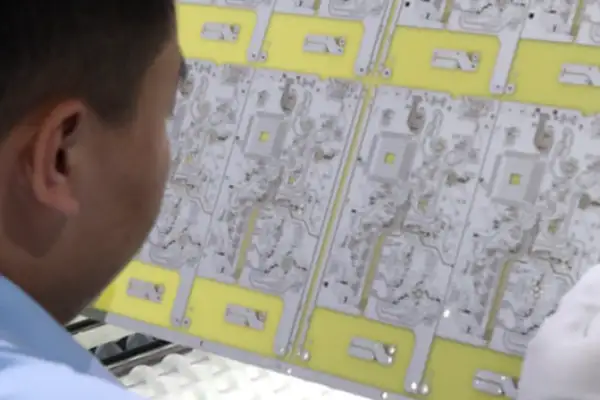
Smart lock control boards integrate fingerprint sensing, Bluetooth or Wi-Fi communication, motor drive control, touch interface processing, cryptographic functions, and power management in a space constrained by the lock body housing dimensions. Standard multilayer PCB technology cannot achieve the routing density this integration requires while maintaining adequate signal isolation between incompatible circuit domains. HDI — high-density interconnect — enables the necessary density through microvias, blind vias, and finer line geometries.
But HDI is not simply making lines smaller. A qualified HDI PCB manufacturer performs the equivalent of micro-scale urban planning on the board. They must determine how to route the fastest-switching signals without creating coupling paths into the most sensitive measurement circuits. They must provide clean, low-impedance power distribution to circuits with very different current profiles — the motor draws ampere-level current for fractions of a second during operation; the fingerprint sensor’s analog front end requires microamp-level stable current continuously. These must coexist on the same board.
One project case made this concrete: a cost-driven design choice to use a four-layer board instead of six resulted in inadequate space to route the wireless module away from the fingerprint sensor’s signal conditioning path. Wireless activity caused visible degradation in recognition performance. Switching to a six-layer design with proper domain partitioning resolved the problem. The additional layer count cost was small relative to the field investigation and redesign cost the four-layer choice eventually required.
Power consumption is another area where PCB quality produces measurable differences. Parasitic capacitance between densely routed traces in a high-density board creates leakage current paths that do not appear in schematic simulation. On a battery-powered device like a smart lock, these leakage paths reduce standby life. A board where adjacent signal lines are separated by inadequate distance may consume measurably more standby current than designed — even though every component specification is met. Discovering this in field deployment rather than during design validation requires expensive remediation.
Power Supply Partitioning for Mixed-Domain Electronics
Smart lock control boards are mixed-domain systems: they contain high-frequency digital circuits, sensitive analog measurement circuits, RF transmitters, and high-current motor drive outputs. The instinct to connect all these circuits to a common supply rail introduces noise from high-current and high-switching-rate domains into sensitive measurement circuits.
The supply voltage for the motor drive section varies significantly during motor operation. The back-EMF when the motor decelerates generates a reverse voltage spike that appears on the supply rail if not properly managed. If this spike reaches the processor supply or the fingerprint sensor analog supply, it appears as a noise event that can cause a measurement error or a processor reset. The design countermeasure is supply domain partitioning: separate regulation for the motor drive section and for the analog and digital circuits, with defined filtering at domain boundaries.
A documented case from field service: a smart lock product exhibited intermittent processor resets that correlated with unlock operations. Because the motor fires during unlock, this correlation was visible but the cause was initially attributed to software. Investigation found that the motor supply spike — approximately 3V above the nominal supply voltage, lasting about 50 microseconds — was appearing on the processor supply rail through inadequate decoupling. Adding a low-resistance ferrite bead in series with the processor supply entry, with appropriate bypass capacitors on both sides, suppressed the spike propagation. The fix cost almost nothing. The field investigation cost much more.
Star-topology grounding prevents ground current from one domain from flowing through the reference ground of another domain. The single-point connection between analog and digital ground, located as close as possible to the ADC reference, ensures that digital switching return current does not flow through the measurement reference. This is a layout discipline, not a component addition — it requires explicit routing decisions, not reliance on default ground plane behavior.
Touch Interface Signal Protection
Capacitive touch interfaces for smart lock access control detect small changes in capacitance produced when a finger approaches a touch pad. The detection circuit measures capacitance changes that may be in the femtofarad range. Any interference coupling into the sensing conductor at the relevant frequencies degrades detection reliability.
The motor drive circuit generates electromagnetic disturbance at switching frequencies and harmonics when the lock actuates. If the touch interface signal trace routes in proximity to motor drive conductors, the switching noise couples into the touch detection path. The result: inconsistent touch response, phantom touches during motor operation, or reduced touch sensitivity that causes users to need multiple attempts.
Proper touch interface protection in layout requires placing the capacitive sensing traces in a dedicated routing region separated from power switching conductors, surrounding sensing traces with a grounded shield pour, minimizing trace length from the sensing pad to the detection IC, and ensuring the sensing trace does not cross any power conductor — even in perpendicular orientation — over a split in the reference plane.
A case that combined several of these failure modes: a smart lock design with the touch keypad traces routed directly over the motor drive traces on adjacent layers, with inadequate shielding. Touch response was unreliable when the motor was active or had recently been active. Board-level thermal effects from the motor current also affected touch sensitivity by changing the dielectric characteristics of the FR4 substrate in the motor drive area. Rerouting the touch traces to a separate board region and adding a complete ground plane layer between the touch domain and the motor domain resolved both problems.
Environmental Resistance Over Service Life
Smart locks installed on exterior doors experience conditions that laboratory test environments rarely replicate: temperature cycling from winter cold to summer heat, humidity variation that produces condensation on cold surfaces in warm humid conditions, and repeated mechanical shock from door closing and latching. The PCB inside must maintain its electrical characteristics and mechanical integrity across all these conditions for the lock’s expected service life — typically five years or more.
Material selection directly affects service life in these conditions. Standard FR4 absorbs moisture at rates that increase with sustained humidity exposure. In a product installed on an exterior door in a humid climate, moisture absorption over years shifts the dielectric properties of the substrate and reduces insulation resistance between conductors. This affects signal integrity and can accelerate corrosion at exposed metal surfaces.
High-Tg FR4 maintains dimensional stability at temperatures that would cause standard FR4 to soften. For smart locks that may see elevated temperatures from direct sun exposure on metal doors, this stability prevents the mechanical deformation that creates stress at solder joints and component leads. One product failure analysis found that a lock installed on a south-facing exterior door in a warm climate showed progressive failure of solder joints at a specific high-current component after two summers of service. The root cause was thermal cycling stress: the standard FR4 substrate showed dimensional changes under the peak temperature, and the accumulated mechanical stress at the solder joints eventually produced cracking.
Conformal coating applied to the assembled board provides protection against moisture, contamination, and corrosive elements. For smart locks installed in environments with chemical vapor exposure — parking garage fumes, coastal salt air — conformal coating prevents the corrosive attack on copper conductors and solder joints that these environments produce over time. Application quality matters: coating applied inconsistently, with gaps or contaminated areas, provides channels for moisture ingress rather than barriers against it. Selective coating systems that apply material precisely where required and avoid connector contacts and test points produce more consistent protection than spray-and-mask approaches.
Evaluating an HDI PCB Manufacturer for Smart Lock Applications
The questions that reveal genuine capability for this application are not about layer count or minimum line width — these are baseline parameters. The differentiating questions address process understanding and application context engagement.
A capable HDI PCB manufacturer, reviewing a smart lock control board design, asks about the deployment environment: will this be installed indoors or outdoors? What humidity conditions will it experience? The answer changes material selection and coating recommendations in ways that a generic capability review cannot reach.
Process consistency across production batches matters more than first-article performance for a product produced in volume. A manufacturer whose process produces consistent impedance, consistent plating quality, and consistent dimensional accuracy across production batches is more valuable than one whose first samples are impressive but whose production batches show variation. Asking for production data across multiple batches — not just first-article test reports — reveals whether the consistency exists.
The cost of inadequate PCB quality in a smart lock application is not visible at delivery. It appears months or years later as field failures, service calls, warranty replacements, and reputation damage. A lock that fails to open when needed, or that requires repeated attempts in cold weather, is a product failure regardless of the sophistication of its recognition algorithm. The circuit board that allows that failure is the weak link, and it is the link whose quality is determined entirely at the design and manufacturing stage — before any user ever touches it.
The design principle that holds across every variation of this problem: the smart lock’s intelligence is only as reliable as the physical platform carrying it. A well-designed Smart Lock Control Board should be so stable that it becomes invisible to users — it simply works, consistently, through temperature extremes, humidity cycles, and years of daily operation. Achieving that invisibility is the result of taking the circuit board seriously as an engineering product, not treating it as a commodity substrate.
What actually makes a long-term PCB supply chain partnership work — shared
Practical, experience-based strategies for how to reduce PCB procurement risks — from
Real factory-floor lessons on how to optimize a PCB manufacturing process —
- Experto en producción de lotes pequeños y medianos
- Fabricación de placas de circuito impreso de alta precisión y montaje automatizado
- Socio fiable para proyectos electrónicos OEM/ODM
Horario comercial: (de lunes a sábado) De 9:00 a 18:30
Get quote, solution or any question, Andre always here to help