
Battery Monitoring System PCB: Why the Hardware Foundation Determines Everything Else
BMS reliability isn’t decided by algorithms — it’s decided by the PCB
Selecting a reliable PCBA partner is, indeed, a technical undertaking. I have seen far too many projects stumble because the wrong supplier was chosen—whether due to component shortages that brought production lines to a halt, or poor soldering quality that resulted in persistently high product rework rates.
Sometimes, you really cannot judge a supplier solely by the numbers on their quotation sheet. Last year, we had a medical device project where the quotes from two potential suppliers differed by nearly 20%. The lower-priced supplier beat their chest and guaranteed flawless quality; however, during the sample stage, we discovered that their conformal coating was applied unevenly. They later admitted that they were using manual spraying equipment. The level of investment a supplier makes in equipment for such critical process steps often serves as a clear indicator of their professionalism.
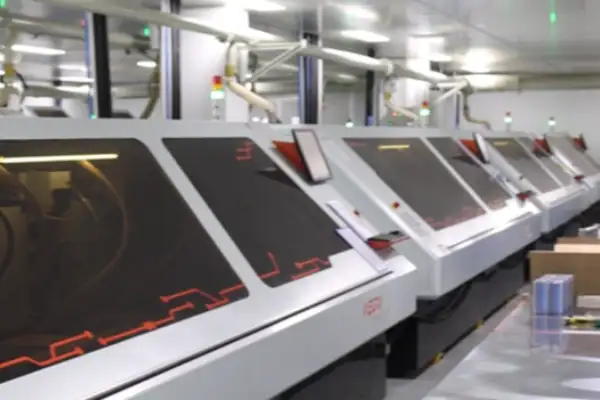
Nowadays, when seeking new suppliers, I place particular emphasis on their willingness to open their production workshops for our on-site inspection. Whether the Automated Optical Inspection (AOI) machines on the assembly line are the latest models, or whether the X-ray equipment undergoes regular calibration—these details are far more convincing than any ISO certification number printed on a certificate. On one occasion, while touring a workshop, I observed workers using microscopes to conduct spot checks on BGA soldering quality; this level of meticulousness regarding details instantly put my mind at ease.
Supply chain resilience is another point that is often overlooked. I recall a long-term PCBA partner of ours that, even during the global chip shortage last year, managed to ensure that 95% of our materials arrived on time. I later learned that they had established a multi-regional procurement network, ensuring that at least three alternative supply channels were secured for all critical components. This kind of proactive, “plan-ahead” mindset is far more valuable than a mere 5% price reduction. I’ve recently been engaging with several PCBA suppliers who claim to offer “flexible manufacturing,” but I’ve found that very few can genuinely achieve rapid line changeovers. One factory, however, showcased an MES (Manufacturing Execution System) that was truly impressive; simply scanning a QR code instantly retrieves the specific process parameter package for a different product—they’ve even managed to streamline the steel stencil replacement process for solder paste printers down to under ten minutes. From a long-term perspective, the efficiency gains driven by this kind of intelligent automation are far more valuable than merely driving down unit prices.
In reality, the most critical factor in determining a supplier’s reliability is observing whether they treat a client’s project with the same meticulous care they would apply to their own proprietary products. Engineers who proactively suggest optimizing layout designs to simplify the component placement process—thereby reducing assembly complexity—are invariably more worthy of long-term trust than teams that merely execute instructions strictly “by the book.” After all, a truly successful partnership is never a zero-sum game between client and vendor, but rather a journey of mutual growth.
Whenever I observe the intricate, densely packed assembly processes of circuit boards, a thought always crosses my mind: sometimes, our over-reliance on machinery causes us to overlook the most fundamental aspects of the craft. Take PCB assembly, for instance: many factories today place almost superstitious faith in Automated Optical Inspection (AOI) systems, believing that simply installing an AOI unit guarantees flawless production. But is that really the case? No matter how sophisticated the technology, it can never truly “see into the human heart”—that is, it cannot replicate human judgment and intuition.
I recall an incident where I happened to be visiting a workshop just as a batch of boards ran into trouble. The AOI system had flagged every single board as “passed,” yet once powered up, the entire batch proved unstable. Eventually, a veteran technician—armed with nothing but a magnifying glass—painstakingly traced the circuitry line by line until he discovered a “cold solder joint” (a poor electrical connection). The defect was located in such an obscure spot that even the X-ray inspection system had failed to detect it. That experience drove home a crucial point: no matter how advanced the automated inspection technology becomes, it can never fully replace the accumulated experience and expertise of human professionals.
Nowadays, the industry is rife with casual talk of “fully automated inspection,” as if simply feeding a circuit board into a machine guarantees 100% reliability. In truth, many subtle defects—such as intermittent failures caused by component aging, or latent risks embedded within the original design—lie beyond the detection capabilities of current automated equipment. Moreover, there are often minute variations in the electrical characteristics of components sourced from different manufacturing batches; how could a rigid, pre-programmed automated system possibly catch such variables?
I’ve encountered engineers who possess an exceptional degree of professional rigor; they will manually conduct supplementary checks at critical junctures—going so far as to deliberately subject the boards to extreme environmental conditions—simply to observe how the circuitry responds. While these “old-school” methods may sound primitive, they frequently uncover issues that standard automated protocols completely overlook. After all, circuits are designed to be used by human beings, not merely to be visually inspected by machines.
Ultimately, technology is merely a tool; true quality control hinges upon a keen sensitivity to detail. It is much like cooking: simply reading a recipe isn’t enough—you have to taste the dish yourself to determine whether it needs a pinch of salt. Over my years of working with circuit boards, I’ve noticed a rather interesting phenomenon: many people approach supplier selection much like browsing a produce market—they fixate solely on the unit price. In reality, it’s quite similar to buying fruit: the cheapest vendor is rarely the one offering the freshest goods.
I learned this lesson the hard way last year. I hired a factory that offered an exceptionally low quote to manufacture a batch of boards; however, during the surface-mount assembly stage, resistors and capacitors were falling off like scattered sesame seeds. I later discovered that their equipment was ancient—the vacuum nozzles were worn smooth, yet they hadn’t bothered to replace them. This sort of hidden material wastage ultimately ended up costing me dearly. What was even more frustrating was that they couldn’t even place 0402 components straight, yet they tried to feed me excuses about “incoming material defects.”
Nowadays, whenever I negotiate with a supplier, I insist on seeing photos of their workshop first. You have to pay close attention to the details—for instance, are the component feeders arranged neatly and uniformly? Are the employees wearing anti-static wrist straps while working? I once visited a factory for an inspection and discovered they had mixed ICs from different production batches together; my heart sank immediately. No matter how cheap a factory with that level of management might be, I wouldn’t dare entrust my business to them.
The testing phase is another major trouble zone. Don’t fall for the bogus claims of “100% inspection”; what really matters is how they handle anomalies. A good supplier will proactively share X-ray inspection images with you, pointing out specific solder joints that might be prone to cold soldering; a poor supplier will simply toss a generic “Certificate of Conformity” at you and call it a day. I now make it a point to require them to perform boundary scans specifically for high-speed signal lines—it’s an expense that is well worth the investment.
The most persistent headache of all is the issue of delivery deadlines. Some suppliers make grand promises when quoting a job, but once production actually begins, they conjure up every excuse imaginable to drag out the schedule. I’ve gotten smarter now: before signing a contract, I demand to see their production schedule and a clear breakdown of their material readiness status. I once had a rush order where the supplier’s project manager actually live-streamed the workshop’s progress directly to me—that is the kind of responsiveness you can truly rely on.
Ultimately, choosing a supplier is akin to finding a business partner; if you base your decision solely on the quoted price, you are absolutely bound to stumble. My guiding principle now is this: I’d rather pay an extra twenty cents per unit to work with a partner who is readily available to communicate and resolve issues—after all, the cost of reworking a batch of defective circuit boards could easily amount to the cost of manufacturing ten new batches.
I’ve spent a fair amount of time inside factories, observing the various stages of printed circuit board assembly. The sight of those high-speed automated machines in action is truly impressive. I recall an interesting phenomenon I observed once while debugging a new piece of equipment: when the vacuum nozzle picked up a miniature resistor, even a slight deviation in angle would cause the entire component to shift out of position. This made me realize that behind seemingly simple actions lie complex physical principles.
Many people assume that automated manufacturing is merely a matter of pushing a button; in reality, every stage requires human intervention. For instance, when switching to vacuum nozzles of different specifications, one must repeatedly test the suction force—too weak, and the component might drop; too strong, and it risks damaging the component itself.
On one occasion, we encountered a thorny issue: a specific type of chip with a unique packaging design was frequently misplacing during the placement process. We later discovered the cause: the nozzle’s design failed to account for the reflective properties of the chip’s surface, leading the vision system to misjudge its position. We were only able to resolve the problem after adjusting the lighting angle.
During the printed circuit board (PCB) assembly process, environmental factors are often the most overlooked element. Fluctuations in the workshop’s temperature and humidity can cause component dimensions to change by a few microns—changes invisible to the naked eye, yet sufficient to compromise placement accuracy.
I often feel that modern equipment places too much emphasis on speed; sometimes, slowing down the pace actually helps reduce the rework rate. After all, a single circuit board contains thousands of components; if just one is placed incorrectly, the entire board may have to be scrapped. The cost of such a failure is far more severe than the cost of taking a few extra minutes.
In truth, the ultimate test of technical expertise lies not in handling routine production, but in managing anomalies. For example, when a component feeder jams, one must quickly diagnose whether the issue stems from a mechanical malfunction or a defect within the component itself. This kind of expertise can only be cultivated through years of hands-on practice.
I have seen far too many companies blindly chase after the latest equipment while neglecting to train their operators. The result is that their advanced machinery ends up performing at nothing more than a basic functional level—much like handing the keys to a sports car to a novice driver and expecting them to drive with professional-level skill.
Whenever I see people treat PCBA contract manufacturing as a simple matter of assembling parts, I feel a sense of regret. Many assume that simply handing a Bill of Materials (BOM) to a factory is all it takes to ensure success; in reality, it is much like giving the same recipe to different chefs—the resulting dishes will inevitably taste completely different. I have witnessed countless teams stumble during the component procurement phase: even when the BOM clearly specifies a standard, widely available model, the supplier might report a stockout. The substitute components procured in a pinch—though technically matching the specified parameters—often fall far short in terms of actual performance.
What truly shifted my perspective on this subject was an urgent troubleshooting project I assisted a friend with last year involving a smart home device. The factory they had contracted had designed the sensor pads on the PCB too densely; consequently, during the reflow soldering process, severe solder bridging occurred. What makes matters worse is that issues of this nature are completely undetectable during the surface-mount assembly process itself; they only surface during the functional testing phase. That experience taught me a crucial lesson: every stage of Printed Circuit Board Assembly (PCBA) is inextricably linked. No matter how elegant the design files may be, if the manufacturing processes fail to keep pace, the entire project is still bound to end in failure.
Nowadays, when communicating with partners, I pay particular attention to their engineering feedback capabilities. A competent PCBA supplier doesn’t merely execute the build mechanically according to the blueprints; instead, they proactively identify potential design pitfalls—for instance, by alerting you that the current PCB layout may be inadequate to meet a specific chip’s thermal dissipation requirements, or by suggesting adjustments to the soldering temperature profiles of adjacent components to ensure greater compatibility. This perspective—optimizing the design by working backward from the manufacturing end—is often far more valuable than simply haggling over a lower unit price for processing.
Recently, I’ve observed a fascinating trend: an increasing number of small-to-medium-sized teams are opting to handle both PCB prototyping and mass production with the same vendor. Doing so not only eliminates the time wasted on repetitive verifications during the transition phase, but—more importantly—it ensures that the manufacturer’s understanding of the design intent remains consistent throughout the entire production lifecycle. When engineers can directly inspect the surface-mount quality of the initial prototype batch, their subsequent adjustments to component placement become far more targeted and effective. The efficiency gains derived from this kind of close collaboration are far more tangible and substantial than any marginal savings achieved merely by minimizing line changeover times.
Ultimately, the reliability of an electronic product is not something that can be simply “filtered out” during the final inspection stage; rather, it is a quality that must be woven into every single detail—from the selection of components in the Bill of Materials (BOM) to the specific soldering processes employed. Instead of agonizing over whether a particular resistor can be sourced for two cents less, it is far wiser to invest that energy into finding a manufacturing partner who truly possesses deep technical expertise.
I have long felt that many people harbor misconceptions regarding the Fabricación de PCB process. They often assume that the job is complete the moment the components are soldered onto the board. In reality, however, the journey from the assembled printed circuit board to the final finished product involves a series of critical details that are all too easily overlooked.
Take the process of “depaneling” (separating individual boards from a panel) as an example. During a factory visit on one occasion, my heart skipped a beat when I witnessed workers manually snapping apart the assembled panels with their bare hands. Those edges, which appeared perfectly neat and uniform on the surface, actually concealed a hidden risk: microscopic cracks. While these micro-cracks might not manifest immediately, they can eventually evolve into catastrophic failure points when subjected to prolonged vibration or mechanical stress.
I place particular emphasis on the “conformal coating” (or “three-proofing”) stage of production, having witnessed far too many instances where skipping this step resulted in costly consequences. In one specific case, a client—in a desperate bid to meet a tight deadline—opted to bypass the conformal coating process. Consequently, after just three months of operation in a humid environment, their equipment suffered from widespread corrosion. Although the electronic components themselves remained functionally intact, the underlying circuitry had been so severely eroded by the moisture that it was rendered completely irreparable. Ironically, the testing phase is the part that gives me the most peace of mind. Modern automated inspection equipment has become quite sophisticated; once a printed circuit board assembly is complete, a system-wide inspection can effectively eliminate over 90% of potential issues. However, I have also observed that some manufacturers rely too heavily on automated testing, thereby overlooking the critical importance of manual re-inspection. After all, machines simply cannot fully replicate the myriad unforeseen circumstances that arise in real-world usage scenarios.
I once encountered a batch of circuit boards that performed flawlessly during functional testing, yet suffered from frequent system crashes once installed in their final devices. It was later discovered that mechanical stress generated during the board separation process had caused latent damage to the pins of a specific chip. Issues of this nature often require a comprehensive analysis spanning multiple stages of the manufacturing process to pinpoint the true root cause.
I view the entire manufacturing workflow as a jigsaw puzzle, where every single piece must fit together seamlessly. Sometimes, the most inconspicuous steps are the ones that best demonstrate a manufacturer’s level of professionalism—for instance, the uniformity of the conformal coating application. Such minute details often determine whether a product will have a service life of three years or ten.
Truly reliable manufacturers do not view each stage of the process in isolation; instead, they begin considering subsequent steps—such as board separation methods and protective measures—right from the initial design phase. This holistic, end-to-end mindset is far more critical than any single technical capability.
I have always found the process of circuit board assembly to be quite fascinating—it is certainly not as simple as merely snapping building blocks together. I recall a particularly memorable experience while touring a factory’s production line: they were grappling with a batch of boards plagued by a high defect rate, all stemming from issues that had occurred during the reflow soldering stage.
That factory had initially assumed that possessing state-of-the-art equipment would be sufficient to guarantee quality. However, they soon discovered that even with the latest model of reflow ovens, various minor defects—such as cold solder joints or component misalignment—continued to occur with alarming frequency. It was only then that they realized the true key lies in the effective integration and seamless transition between every single stage of the entire production workflow. For instance, if the component placement operation is not executed promptly after the solder paste printing stage, the subsequent soldering quality can be severely compromised. Similarly, if the oven temperature control lacks sufficient precision, it can trigger a chain reaction of adverse effects, ultimately undermining the stability and quality of the final product. In reality, we often fall into a common trap: becoming overly reliant on a specific piece of equipment or a particular technical parameter, while overlooking the critical importance of overall process coordination. Take, for instance, an example I observed recently: although adjusting the nitrogen flow parameters did indeed resolve the issue of excessive voiding in some instances, the deeper underlying cause lay in the initial process design phase—specifically, a failure to adequately consider whether the compatibility between the material characteristics and the equipment’s performance was truly appropriate. This reminds me of similar situations I encountered back when I was conducting experiments myself: I would follow the standard operating procedures to the letter, yet consistently fail to achieve the expected results. It was only later that I discovered the culprit was fluctuating environmental humidity, which affected the activity of the solder paste and, consequently, led indirectly to poor soldering quality.
Therefore, whenever I now encounter cases involving defects during the circuit board assembly process, my first instinct is to consider whether there is an inherent flaw or irrationality within the process setup itself, rather than simply attributing the problem to external interference. After all, from the selection of raw materials to the final product inspection, a single oversight at any point along this entire chain can evolve into a potential risk factor. Only by treating each step as a distinct yet interconnected component of the whole can we truly succeed in taking preventive measures and minimizing unnecessary losses.
Of course, that being said, a truly flawless production process is an almost mythical concept. What truly matters—and what we should focus our attention on—is our ability to extract valuable lessons from every problem we encounter and to continuously optimize and refine our processes.
Whenever I see those neatly arranged electronic components mounted on a circuit board, I am reminded that, beneath the surface, this entire operation is essentially a game of precision. Many people assume that the most complex aspect of Printed Circuit Board Assembly (PCBA) is the high-speed operation of the pick-and-place machines; however, I would argue that the true test of skill lies in the application of that thin layer of solder paste. If this initial step is executed poorly, even the most sophisticated equipment used in subsequent stages will be rendered completely useless.
I have seen far too many novice engineers fixate solely on equipment parameters while completely overlooking the fundamental characteristics of the materials they are using. Take the selection of solder paste, for instance: materials with different viscosities behave—and feel—completely differently as they flow across the stencil. Sometimes, the issue isn’t with the machine itself, but rather that the wrong material was chosen from the very start. That subtle, tactile sensation is akin to whipping cream when baking a cake—a fraction too much or too little can completely alter the final outcome.
I recall an instance where I was troubleshooting a production line: although every parameter met the required specifications, we kept encountering welding defects. We eventually discovered that the airflow from the workshop’s air conditioning was blowing directly onto the printing area, causing the surface of the solder paste to dry out slightly. Such minute details are never documented in operation manuals, yet their practical impact can be severe enough to render an entire batch of products unsalvageable. Consequently, I have developed a habit: whenever I enter the workshop, I now take a moment to gauge the temperature and humidity before I begin my work.
The design of the stencil—the metal mask used for solder paste printing—is actually quite an interesting subject. Some people blindly pursue extreme thinness, believing that the thinner the stencil, the greater the precision. However, in reality, one must strike a balance based on the component layout. For instance, in situations where large capacitors and tiny resistors coexist, specific areas of the stencil may require localized thickening. The logic here is much like that of a tailor crafting a garment: different parts of the outfit require different cutting techniques to ensure a perfect, contoured fit to the body.
The rhythm and timing of the printing process itself require considerable finesse; moving too quickly can lead to “stringing” (solder paste trailing), while moving too slowly can compromise efficiency. I typically observe the way the solder paste forms within the stencil apertures—much like watching the flow of milk foam as a barista creates latte art. Mastering that delicate balance requires repeated practice and refinement.
What strikes me most about this industry is that, even as our equipment becomes increasingly intelligent, many critical judgments still rely heavily on human experience. On one occasion, the automated inspection system indicated that everything was in perfect order; yet, I couldn’t shake the feeling that the luster of the solder paste in a specific area looked slightly off. I insisted on conducting a manual re-inspection, and sure enough, I discovered a problem involving tiny air bubbles. This kind of intuition is difficult to explain through data alone, yet it often serves to avert major catastrophes.
I have seen far too many people oversimplify the complexities of PCBA manufacturing. They tend to assume that simply finding the vendor offering the lowest quote will suffice—that is, until the first batch of boards arrives with a staggering defect rate of 30%, at which point they finally realize just how many hidden pitfalls lie beneath that “cheap” price tag.
Take, for instance, a startup we collaborated with just last month. In an effort to save a mere few thousand dollars, they chose a small, makeshift workshop to manufacture the mainboards for their smart wristbands. The result? Out of the initial batch of 200 units, more than 60 suffered from cold solder joints. Not only did the rework process cost them two weeks of precious time, but they also had to re-order components—and those chips, purchased in such small quantities, ended up costing 40% more than the standard bulk rate. And that’s not even mentioning the financial penalties they incurred from their clients due to the delayed delivery.
Many people fail to realize that the “hidden costs” of PCBA manufacturing are often buried deep within the details. For example, one client insisted on using a specific model of component feeder, claiming it offered superior performance. However, that particular feeder proved incompatible with our production line; every time we switched product lines, we had to spend half a day troubleshooting and recalibrating, causing our production throughput to plummet by 50%. Such losses in efficiency ultimately translate directly into higher overall costs.
I recall an even more outlandish experience: a specific batch of boards passed every internal test with flying colors, yet once they reached the client’s end, they began crashing frequently. We spent three days poring over production records before finally discovering the culprit: the storage temperature for one specific reel of ICs had exceeded the permissible limit. Although the chips themselves hadn’t suffered immediate physical damage, exposure to such high temperatures had drastically shortened their operational lifespan. Issues of this nature would be virtually impossible to detect without a comprehensive traceability system in place.
Nowadays, whenever I review a PCBA quotation, I pay particular attention to a few key areas. First is the handling of engineering changes; some factories charge exorbitant fees for every design revision. Second is material management fees; many manufacturers pass their warehousing costs directly onto the client. Most importantly, I scrutinize the quality control standards, as the costs associated with different levels of inspection can vary significantly.
In truth, selecting a supplier is much like choosing a spouse: you shouldn’t focus solely on the “dowry”—the initial price tag—but rather on whether they can reliably accompany you through the entire product lifecycle. Those who aggressively undercut prices right from the start often cut corners in ways you cannot see, whereas a reliable partner will proactively help you anticipate and mitigate potential risks in every single production batch.
We are currently assisting a medical device client with a product upgrade. Their requirements mandate a “zero-defect” standard, necessitating X-ray inspection and boundary scanning for every single PCBA unit. Naturally, such rigorous quality demands are reflected in the quotation; however, the client fully understands that—compared to the potential risks and costs of a product recall down the line—this investment is absolutely worth it.
Ultimately, a successful PCBA partnership must be a two-way street. On one hand, the factory must maintain full transparency regarding all cost components; on the other, the client must recognize and value the expertise and professional services being provided. After all, no business can survive for long while operating at a loss; the foundation of any enduring partnership lies in ensuring that both parties receive a fair and reasonable return.
I have encountered far too many people who oversimplify the PCBA process, imagining it to be nothing more than placing a pile of components onto a circuit board and running it through an oven. This mindset is actually quite dangerous, as it overlooks the true challenges and complexities inherent in the manufacturing process. Every time I witness a bare circuit board transform into a fully functional electronic device, I feel as though the transformation itself is nothing short of magic.
I recall a specific project where we nearly stumbled at the reflow soldering stage. At the time, everyone was convinced that the temperature settings were perfect; yet, when the first batch of boards emerged, several components were found to be poorly soldered. After hours of troubleshooting, we finally discovered that the reflow temperature profile had not been properly calibrated. That incident taught me a valuable lesson: assembly is not merely about placing components onto a board; every single step of the process requires meticulous oversight.
Nowadays, many people rely too heavily on automation equipment, assuming that machines can handle everything. However, I firmly believe that even the most sophisticated machinery still requires human supervision. Take surface-mount placement, for instance: machines can occasionally “act up,” misaligning components or missing them entirely. If no human operator detects these errors in time, it becomes too late to rectify the issues once the boards have passed through the reflow oven. That is why I always tell my team: don’t just stare at the data on your screens; go walk the production floor, feel the temperature of the boards with your own hands, and use a magnifying glass to inspect the solder joints.
There is another interesting point: different people can have completely different impressions of the very same circuit board. Some feel that as long as the functionality is sound, nothing else matters. I, however, always prefer to hold the board up to the light—examining the luster of the solder joints and checking whether the component alignment is neat and orderly. Such details often serve as a true reflection of the overall quality level of the entire production process. Sometimes, a seemingly insignificant minor issue may actually mask a major flaw in the underlying process control.
Nowadays, I place particular emphasis on pre-production preparation. Take stencil design, for instance: many people view it as nothing more than a simple template. Yet, I have found that even a slight adjustment to the size or shape of the apertures can result in vastly different soldering outcomes. Then there are the component storage conditions; if humidity control is inadequate, even the most brilliant design becomes entirely futile. When combined, these seemingly trivial details often determine the ultimate success or failure of an entire project.
In truth, after working in this field for a while, you come to realize that a high-quality PCBA isn’t achieved through a single standout stage, but rather by ensuring that every single stage is executed flawlessly.
From the initial material preparation to the intermediate assembly process, and finally to the concluding testing and inspection—every single step must be executed with meticulous care and a steady hand.
Sometimes, moving a little slower is actually preferable to rushing the work, as the cost of rework is often far higher than that of standard production.
One habit I have cultivated is to spend half a day on the production line whenever a new product is about to launch.
Watching the boards progress through each successive stage of the manufacturing process gives me a genuine sense of assurance.
This kind of firsthand experience feels far more authentic than simply reading reports. After all, no matter how detailed the data may be, it can never quite compare to witnessing—with your own eyes—the transformation of raw circuit boards into finished products.
Perhaps that is precisely why I have always felt that working in this field requires not only a solid technical foundation but also that distinct spirit of meticulous dedication—the kind of earnestness one typically associates with a true artisan.
BMS reliability isn’t decided by algorithms — it’s decided by the PCB
Beamforming performance depends on phase coherence across every antenna element — and
A relay control board that works perfectly in the lab can fail
- Experto en producción de lotes pequeños y medianos
- Fabricación de placas de circuito impreso de alta precisión y montaje automatizado
- Socio fiable para proyectos electrónicos OEM/ODM
Horario comercial: (de lunes a sábado) De 9:00 a 18:30