
Why the Circuit Board Beneath the Camera Determines Whether Your Surveillance System Holds Up for Years
When selecting components for a security monitoring system, most attention goes to
Having worked in this industry for over a decade, I’ve found that many people’s understanding of aerospace PCBs remains superficial. They always think that simply making ordinary industrial boards thicker and using more robust materials is enough, but that’s not the case at all.
I remember once visiting the workshop of an aerospace PCB manufacturer, where they showed me a board used in satellites. It looked ordinary, but there was a lot more to it than meets the eye. What impressed me most was the special FR material they used, which was completely different from what we usually encounter. This material not only needs to withstand high temperatures but also maintain stability in a vacuum environment. For example, in the space environment, materials face the dual challenges of atomic oxygen corrosion and ultraviolet radiation; ordinary materials would delaminate or experience performance degradation. Aerospace-grade materials, however, need to pass stringent radiation resistance certifications, with a glass transition temperature of at least 180°C, and some even exceeding 200°C.
I’ve seen too many projects fail because of choosing the wrong substrate. One team developing a drone navigation system used ordinary FR4 material to save money, resulting in a sharp decline in performance under high-altitude, low-temperature conditions. They only solved the problem by switching to specialized aerospace PCB material, but by then, they had already wasted six months. In reality, at an altitude of 10,000 meters, temperatures can plummet to -55°C, while also having to withstand low air pressure and vibration. The dielectric constant of ordinary materials changes drastically with temperature, leading to unstable signal transmission delays, which is fatal to the accuracy of navigation systems.
What truly changed my perspective on aerospace PCBs was my experience participating in a rocket control system. It was then that I realized this wasn’t just a circuit board issue, but a problem of the entire system’s reliability. Every solder joint and every trace must be considered for performance under extreme conditions. Sometimes, to be absolutely certain, we even incorporate redundancy in the design phase, even if it significantly increases costs. For example, we use a dual-channel backup design on critical signal lines, so that if one fails, the other can immediately take over. This design approach requires system-level simulation analysis to ensure that redundant paths do not interfere with each other.
Now, whenever I take on a new aerospace PCB project, I first clarify the application scenario. Is it in low Earth orbit or deep space? What temperature difference will it withstand? Are there any special radiation resistance requirements? These factors directly determine the choice of materials and processes. For example, deep space probes need to cope with stronger cosmic rays, requiring substrate materials doped with special elements to shield against radiation effects. Low Earth orbit equipment, on the other hand, must focus on resistance to atomic oxygen corrosion.
Speaking of manufacturing processes, I think the most challenging aspect is controlling weight while ensuring reliability. The aerospace industry is particularly sensitive to weight; even a gram increase can affect overall performance. This requires meticulous layout design, ensuring signal integrity while maintaining a streamlined design. We often use buried resistors and capacitors (BRCs) to embed passive components within the board, saving surface space and reducing overall thickness. Sometimes we also use rigid-flex boards, employing flexible materials in bending areas to reduce weight and improve shock resistance.
A recent project I’ve been working on is quite interesting. The client needed to maintain signal stability under extreme temperature variations, and several solutions we tried were unsatisfactory. We finally solved the problem by changing the laminate structure and using a special FR substrate. This process reinforced my belief that there are no one-size-fits-all solutions in this field; each project requires a customized approach. Specifically, we used a symmetrical laminate design to offset thermal stress deformation, while placing grounding layers around critical signal layers to form complete electromagnetic shielding. While this structure increases manufacturing difficulty, it effectively suppresses signal jitter caused by temperature changes.
Ultimately, what’s most needed in aerospace PCB design is patience and accumulated experience. Unlike consumer electronics, it doesn’t allow for rapid iteration; every detail must be repeatedly verified. But it’s precisely this rigorous attitude that gives this industry its unique charm.
Recently, after working on some aerospace projects, I realized that aerospace PCB design is completely different from ordinary circuit board design. Many people think that simply drawing the circuitry is enough, but what truly determines success or failure are often the unseen details.
I remember a friend who manufactures aerospace PCBs showing me photos of their workshop. The entire production line operated in a cleanroom, and the workers in protective suits reminded me of a hospital operating room. He said that even a single speck of dust on a circuit board could cause a short circuit—this level of rigor is truly awe-inspiring.
Multilayer board design is particularly demanding. Once, when our team was designing a power system, we discovered that a standard layering scheme caused electromagnetic interference. We had to readjust the ground plane layout to solve the problem. This experience made me realize that the biggest fear in aerospace PCB design isn’t technical difficulties, but rather neglecting details.
The design of power modules is also very sophisticated. The temperature difference in the space environment can reach hundreds of degrees Celsius, which ordinary voltage regulator chips simply cannot withstand. We tested dozens of materials and finally chose a ceramic substrate, which, although five times more expensive, demonstrated excellent stability under extreme temperatures.
What impressed me most was a visit to the assembly workshop where I saw workers inspecting solder joints under microscopes, checking each connection point three times over. This almost obsessive quality control process initially seemed like overkill, until a satellite project suffered a system failure due to a single faulty solder joint, and I understood the necessity of such rigorous requirements.
Now, every time I design a new board, I ask myself several questions: How many thermal cycles can this component withstand? Has the spacing between the traces taken into account material aging? I even put samples in a temperature chamber to simulate extreme environments for testing. These seemingly redundant tasks often prevent major losses at critical moments.
I’ve seen too many people think of aerospace PCBs as something too mysterious. Whenever the work of aerospace PCB manufacturers is mentioned, people always think they’re doing something unfathomable. But those who have actually worked in this industry will find that the most crucial element is never some magical technological breakthrough, but rather that almost obsessive attention to detail.
I remember visiting an Aerospace PCB manufacturing plant once. An engineer pointed to an ongoing vibration test and told me that this seemingly simple, repetitive action involved countless parameter adjustments. Many people think this kind of testing is just a formality. But in reality, every step can expose blind spots in the design.
I particularly admire teams that truly understand the value of testing. They don’t waste time boasting about how advanced their technology is; instead, they honestly admit that even the best design needs to withstand the test of real-world environments. I once saw a very interesting way they handled a signal integrity issue—instead of rushing to change materials or redesign, they first analyzed the abnormal fluctuations in the test data.
Many manufacturers now like to emphasize how advanced their substrate materials or how precise their soldering processes are. But what truly determines whether a PCB can work stably in extreme environments is often the most fundamental thing: for example, whether thermal expansion and contraction margins were considered during routing, and whether the pad design included sufficient safety margins.
One detail that impressed me deeply was their attention to detail during high-temperature aging tests. They not only recorded changes in electrical performance but also used microscopes to observe subtle changes in the solder joint interfaces. This focus on detail is the attitude a truly trustworthy aerospace PCB manufacturer should possess.
Ultimately, the biggest danger in this industry is making assumptions. Parameters you calculate might not be what they seem in a real vibration environment; perfect signal transmission in the lab might experience unexpected attenuation in a vacuum. This is why I firmly believe that reliable aerospace PCBs are not designed but tested—every test is a dialogue with the laws of physics, not a verification of theoretical formulas.
Teams that can accept test results, even less-than-ideal ones, are more likely to produce truly reliable products because they understand how to respect objective laws rather than obsessing over proving their own superiority.
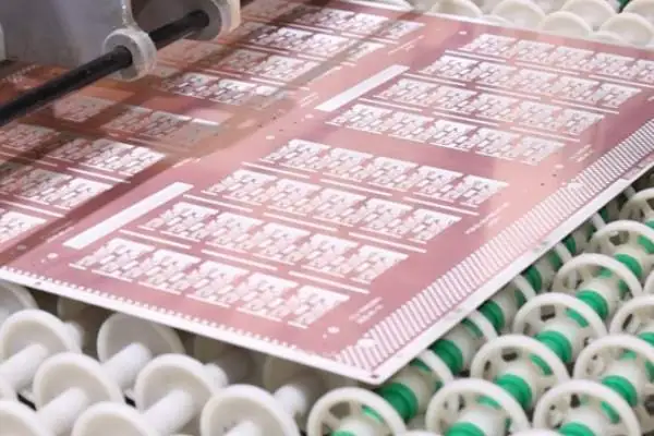
I’ve always found circuit board design in the aerospace field particularly fascinating. Last year, I visited a factory specializing in aerospace PCBs and discovered that the industry is far more complex than I imagined. They showed me a multi-layer board used in satellites, less than a third the thickness of a fingernail, yet capable of stable operation in a vacuum environment for over ten years. These circuit boards undergo rigorous ion contamination testing to ensure they won’t leak or short-circuit under long-term radiation. Manufacturing also takes place in cleanrooms, as even a single speck of dust can cause signal transmission abnormalities.
Traditionally, aerospace-grade products are thought to require the heaviest materials, but now the focus is more on precision packaging technology. Embedding components like processors and sensors into high-density substrates like building blocks is more reliable than simple stacking. I’ve seen some aerospace PCB designs that even embed chips directly into the substrate, saving space and reducing external interference. For example, blind via technology allows for over 20 layers of circuitry, while special filler materials completely encapsulate the chips, forming an electromagnetic shielding layer. This three-dimensional integration process allows the circuit board to maintain functionality even after withstanding a 5000G impact.
Recently, I spoke with some engineers and discovered they’re starting to use AI-assisted circuit layout design. One interesting example is that to cope with the extreme temperature differences of a Mars mission, they simulated hundreds of material combinations using algorithms, ultimately selecting a ceramic substrate that remained stable between -150°C and +120°C. Such experiments, relying on manual trial and error, could take years. AI systems can also optimize wiring paths, controlling the length of critical signal lines with millimeter-level precision to avoid timing errors caused by temperature differences. Some design software can already automatically detect points of thermal stress concentration and recommend the optimal component arrangement.
In fact, the space environment tests not individual performance but overall coordination. I remember once seeing a deep space probe almost fail because a solder joint on a regular PCB expanded due to heat; the manufacturer later solved the problem by using flexible printed circuits. Now I realize that advancements in aerospace often stem from these kinds of meticulous details. Modern flexible circuits use polyimide substrates, which can be bent and folded like paper, making them particularly suitable for installation in the irregular cabins of spacecraft. One company has even developed stretchable circuits that maintain conductivity even when the device deforms.
Sometimes, when watching live rocket launches, I pay special attention to the electronic equipment inside the rocket; they don’t use ordinary circuit boards. After all, in a weightless environment with strong radiation, even the current flow changes, not to mention the need to consider heat dissipation and shock resistance. Some private aerospace companies are now surprisingly finding success with lighter packaging solutions, such as making the entire control system into a postage stamp-sized module. These modules use a metal core substrate and microchannel liquid cooling technology, weighing only one-tenth of traditional solutions. One power management module for microsatellites, only 1.6 millimeters thick, integrates 32 functional units.
I’ve always believed that the most fascinating aspect of this industry is its constant self-challenge. Even when 99.99% reliability is achievable, they strive for another 9; even with mature solutions, they explore new materials. For example, a team recently researched integrating neural network processors directly onto aerospace PCBs—a risky endeavor, but if successful, it would allow satellites to autonomously determine cloud thickness to decide whether to take pictures and transmit data. They are also experimenting with coating the circuit board surface with nanoscale diamond films, a material that is both radiation-resistant and has excellent thermal conductivity. Some labs are testing the use of graphene to create antenna circuits that can be directly printed onto the spacecraft’s outer shell.
Ultimately, aerospace circuit boards are no longer just carriers of connected components; they’re more like precision armor protecting humanity’s dreams in extreme environments. Every millimeter of wiring can determine the success or failure of the entire mission. This pressure and sense of accomplishment are probably the driving force behind the industry’s continuous breakthroughs.
I’ve seen too many people overcomplicate aerospace PCBs. The key isn’t how many high-end technologies are used or how many test certificates are passed—what truly matters are the meticulous attention to detail.
I remember once visiting an aerospace PCB manufacturer’s workshop. They showed me a board that was about to be scrapped. The surface looked perfect, but there was a tiny air bubble inside. This kind of problem might be insignificant on ground equipment, but in the space environment, it would be a ticking time bomb. This made me realize that true quality control isn’t about final inspection, but about maintaining vigilance in every process.
Many people think verification is just going through the standard procedures. But the most valuable parts often happen in unexpected situations. For example, during temperature cycling testing, we deliberately added a sudden change beyond the specifications in one cycle, and found a tiny crack in the solder joint of a certain component. This extreme situation, although unexpected, exposed a material incompatibility issue.
When selecting components, I prioritize a supplier’s actual case studies over theoretical specifications. One manufacturer supplied capacitors that, while nominally meeting aviation standards, showed significant performance degradation under long-term vibration. We switched to another supplier whose products had been proven in actual flights, even though the price was three times higher – it was worth it.
Many of my peers now focus on pursuing the latest technologies, but I believe mature and stable solutions are more reliable, especially in the aerospace field. Sometimes, the simplest epoxy resin encapsulation guarantees long-term reliability better than fancy new materials. The key is to perfect the basic processes.
What impressed me most was seeing our PCBs remain perfectly still during rocket vibration tests at the launch site. That sense of security was more real than any certification. After working in this industry for a while, you realize that true quality lies in the unseen details.
I recently chatted with an engineer working on a satellite project and noticed something interesting. Their team, in an effort to meet deadlines, tried replacing some aerospace-grade chips with consumer-grade components, nearly causing the entire project to fail. This incident made me rethink what high reliability truly means—it’s never simply about piling on the most expensive parts; it’s about the entire system’s ability to operate stably under extreme conditions. For example, during satellite launch, components must withstand vibration accelerations of up to 20G, while the packaging structure of consumer-grade chips might detach under such mechanical conditions. More importantly, the cumulative radiation dose in space accumulates over time. Aerospace-grade chips have unique radiation-resistant designs that ensure an error rate of less than one in a million within ten years, while ordinary chips might experience bit flips within three months.
Many people believe that aerospace PCBs are simply gold-plated with thick copper foil, but in reality, radiation in the space environment is the real hidden killer. During a visit to a lab, I saw them simulate the destructive effects of space radiation on circuit boards. Ordinary commercial PCBs showed signal malfunctions within minutes of exposure, while specially designed aerospace PCBs could operate continuously for years. This difference cannot be achieved by simply piling on materials; it requires optimization across the entire chain, from routing rules to shielding layer structure. Lab engineers demonstrated how to reduce common-mode interference through differential pair routing and how to insert a ground plane between the power and signal layers to create a Faraday cage effect. They also showcased a special via design where the inner walls of these vias are plated with copper and filled with conductive epoxy resin, forming a continuous electromagnetic shielding channel.
Currently, commercial aerospace companies like to emphasize rapid iteration, but directly applying consumer electronics methods to the space domain will cause problems. I’ve seen a startup’s satellite, using an unverified civilian-grade PCB, suffer a system reboot due to a single-event event after only three months in orbit. True innovation should focus on optimizing processes while ensuring reliability, such as replacing some physical tests with more accurate simulations, rather than blindly pursuing speed. For example, a research institute developed a multiphysics coupling simulation platform that can simultaneously simulate the combined effects of radiation, thermal cycling, and mechanical stress on circuit boards, compressing the traditional three-month environmental test into a two-week process. However, this requires establishing an accurate material degradation model.
The PCBs used on Mars rovers are particularly interesting; they must cope with not only radiation but also enormous temperature differences. A designer told me they embed temperature sensors in the circuit boards to adjust power distribution in real time. This dynamic adjustment capability is more important than simply enhancing heat dissipation. After all, on Mars, you can’t replace parts as easily as on Earth; each component must learn to take care of itself. Their thermal management strategies include embedding shape memory alloys in critical areas of the circuit board. When local overheating is detected, these alloys change shape to trigger backup heat dissipation pathways. They also design microchannels under power devices to utilize carbon dioxide in the Martian atmosphere for phase-change cooling.
What I’m most optimistic about for the next decade is the cross-industry collaboration between traditional aerospace PCB manufacturers and new materials companies. For example, some teams are experimenting with combining flexible circuits with ceramic substrates to maintain radiation resistance while reducing weight. This innovation doesn’t come from simply stacking technical parameters but from truly understanding the actual needs of electronic devices in the space environment—after all, even heat dissipation needs to be redesigned in a vacuum environment. A recent breakthrough involves using carbon nanotube-reinforced polyimide substrates, whose thermal conductivity is 50 times that of traditional FR-4 material. Furthermore, the directional arrangement of carbon nanotubes achieves anisotropic thermal conductivity, precisely directing heat to the spacecraft’s outer shell.
Sometimes, I find the most fascinating aspect of the aerospace field to be its constant balancing act between seemingly contradictory demands: extreme reliability, cost control, decades-long durability, and compatibility with new technologies. This art of balance is far more challenging and truly showcases the wisdom of engineers than pursuing any single metric. For example, designers might use gold-bonded wires in critical signal paths and gold-plated copper wires in non-critical areas, ensuring reliability while controlling costs appropriately. Another example is the “derating” strategy used in component selection, allowing industrial-grade chips to operate within 30% of their nominal parameters in aerospace environments, mitigating component-level risks through system-level safeguards.
I’ve always found PCB design in the aerospace field particularly fascinating; the extremely harsh environments push the limits of human manufacturing. I remember chatting with a friend who manufactures aerospace PCBs. He said their biggest headache wasn’t the single high or low temperature environment, but the constant, fluctuating temperature changes. Imagine a board going from a shaded area at tens of degrees below zero to a scorching hot area under direct sunlight—this temperature difference is torture for the materials.
Different materials on a PCB have vastly different coefficients of thermal expansion; copper foil, epoxy resin, and fiberglass all expand and contract at different rates. The most vulnerable parts are the through-hole structures; the constant temperature changes are like constantly stretching these tiny connection points. I’ve seen some boards recovered from satellites.
Every time I see those precision instruments operating in space, I find it incredibly fascinating. The circuit boards in these devices are completely different from what we use every day. I remember visiting an aerospace PCB manufacturer’s workshop once; they showed me a board used in satellites—its copper foil was more than twice as thick as that of ordinary products, and it felt like a metal bookmark.
The impact of high-temperature environments on materials is beyond imagination. The resin used in ordinary circuit boards releases gas in a vacuum.
I’ve always found those circuit boards that can fly in the sky particularly fascinating. You know, the stuff used in airplanes and satellites is completely different from what we use in our everyday phones. I once visited an aerospace PCB manufacturer’s factory and saw how they tested their products; that’s when I truly understood how sophisticated this stuff is. They don’t just simply test whether it powers on or off; they put the boards in a chamber that simulates the high-altitude environment and subject them to repeated stresses. In that environment, ordinary circuit boards would probably fail long ago. The test chamber precisely controls the air pressure down to stratospheric levels, while the temperature rapidly cycles between -55°C and 85°C, simulating the dramatic temperature changes from the poles to the equator.
Actually, many people don’t understand the special requirements of aerospace. I remember an engineer telling me that their biggest headache wasn’t the technology, but the material selection. Ordinary PCB materials work fine on land, but their true colors are revealed at high altitudes. Not only are there huge temperature changes, but there’s also various forms of radiation interference. It’s like suddenly sending someone accustomed to a greenhouse to live in the Arctic—it’s normal that they can’t adapt. Therefore, manufacturers specializing in aerospace PCBs all need their own proprietary formulas, with everything from the substrate to the coating custom-designed. For example, they might use polyimide substrates instead of ordinary FR-4, as this material performs better in terms of thermal expansion coefficient and dielectric stability.
The most extreme example I’ve seen was a pre-launch test for a satellite. They placed the finished aerospace PCBs on a vibration table and vibrated them continuously for several days, with the frequency constantly changing. At the time, I thought this wasn’t testing; it was torture for electronic products. But later I learned that this kind of rigorous testing was necessary, since the noise and vibration during rocket launch are far more intense. If it couldn’t even pass this test, it wouldn’t be able to go into space. Vibration testing simulates the low-frequency sine waves and high-frequency random vibrations during launch, ensuring that every solder joint and connector doesn’t loosen under continuous acceleration.
Now, many companies are starting to pay attention to this issue because it’s not just the aerospace field that requires such high-reliability products. For example, the environments of communication base stations in remote areas or offshore drilling platforms are also quite harsh. Although not as extreme as space, wind, sun, and salt spray corrosion still pose a significant challenge to ordinary circuit boards. Therefore, these experiences can actually be applied to many more fields. In base stations in desert areas, circuit boards must withstand diurnal temperature variations and sandstorms, while offshore platforms require special protection for metal components against salt spray corrosion.
Ultimately, the most important thing in this industry is a sense of awe. Every time I design a new aerospace PCB, I remind myself that this thing will be working in the sky in the future, and there can be no room for error. After all, problems on the ground can be repaired, but if it’s at tens of thousands of meters in the air or in outer space, it’s truly hopeless. This sense of responsibility makes me extremely meticulous about every detail; sometimes even my colleagues think I’m too fussy. But I believe that if you’re going to do something, you have to do it to the best of your ability, especially when it comes to safety, you absolutely cannot compromise. We conduct rigorous DFMEA analyses to predict every potential failure mode and its impact, ensuring the design is flawless.
Recently, a new project has particularly excited me: developing a control system for a high-altitude unmanned aerial vehicle (UAV). Although it doesn’t need to fly out of the atmosphere, ensuring stable operation under different climatic conditions is still a challenge. We tried several solutions before finding the most suitable material combination. This process has further convinced me that environmental adaptability is the core competitiveness of aerospace. Advanced features alone aren’t enough; the key is to withstand extreme conditions. For example, in high-altitude regions, it’s necessary to address arcing caused by low air pressure, while in tropical rainforests, it’s crucial to prevent mold growth that could affect circuit performance.
Seeing the circuit boards I helped design perform stably in various rigorous tests is quite rewarding. Although this field has high barriers to entry and is very stressful, the satisfaction of successfully solving a problem is unparalleled by other projects. Perhaps it’s precisely because I know these boards will be used in extraordinary places that I put in extra care.
I’ve always found the circuit boards in the aerospace field particularly fascinating. They’re not as casual as the boards in our everyday phones or computers. Every time I see those complex circuit layouts, I wonder how many stories lie behind them. Aerospace PCB manufacturers face far more than simply printing circuits; they have to consider many things we usually overlook. For example, a board has to switch between temperatures of tens of degrees below zero and hundreds of degrees Celsius, and withstand severe vibrations—under such conditions, ordinary design approaches simply won’t work.
I know an engineer in this field who says his biggest headache is finding a balance point under various extreme conditions. You can’t just pursue performance; you also have to consider reliability, cost, and timeline. These four aspects are like a quadrilateral, mutually reinforcing and indispensable. Sometimes, to increase stability even slightly, you might have to readjust the entire circuit design or even start over. This process sounds grueling, but he says it’s the norm. For example, they designed a power module for a satellite, conducting hundreds of thermal cycling tests to ensure perfect material expansion coefficient matching.
Human exploration of space actually relies heavily on these seemingly insignificant boards. Without them, probes simply couldn’t take pictures on Mars or transmit data. I remember reading a report once about a probe almost failing its mission due to a problem with a small circuit board; I felt then that the importance of this thing was underestimated. It’s not just a component; it’s crucial to the success of the entire mission. For example, the Curiosity rover’s computer board uses a triple redundancy design, maintaining basic operation even if two systems fail.
I think people in this field are somewhat idealistic; they know they’re serving a larger goal. While daily work might involve repeatedly testing parameters or adjusting circuit routing, the sense of responsibility felt when considering these boards might fly into space or be used in critical aerospace equipment is quite moving. This isn’t a job anyone can do; it requires not only technical skills but also a meticulous attention to detail. They even use electron microscopes to inspect solder joint quality, recording and analyzing deviations as small as 0.1 millimeters.
Sometimes I wonder why these aerospace PCBs can’t be made simpler. Then I realized that the more complex the environment, the more precise the design needs to be. Like building blocks, each piece must be placed correctly, otherwise the entire structure will be unstable. This is probably what makes it so appealing—always pushing the limits while remaining grounded in reality. For example, spaceborne circuits need to balance radiation resistance and lightweight design, employing special processes like gold wire bonding and ceramic substrates.
I’ve seen many people emphasize high-end technical parameters when discussing aerospace PCBs, but what truly determines success or failure is often the most basic design thinking. Once, I talked to a friend who works with an aerospace PCB manufacturer about a batch of boards they scrapped—not because of substandard materials or manufacturing errors, but because the designer neglected to match the coefficients of thermal expansion during layout. Can you imagine? In a vacuum environment with temperature differences exceeding 200 degrees Celsius, even the slightest difference in expansion and contraction between the ceramic capacitor and the FR4 substrate can cause solder joints to crack. This kind of detail is the Achilles’ heel of aerospace PCB design.
Many people associate redundancy with stacking repetitive circuit modules. However, true redundancy should have a compensatory mechanism, like the human nervous system. In a satellite power module I worked on, the main control chip and the backup chip were not even the same model—they came from different manufacturers and even used different architectures. This heterogeneous redundancy is smarter than simply copying two identical sets of hardware; after all, cosmic rays can cause transistors with a specific structure to collectively fail. True fault tolerance is not simply adding more components but building an ecosystem.
Speaking of derating, I’ve found that novice engineers easily fall into dogmatism. Once, during a circuit review, I saw someone leave 80% power margin for ordinary resistors but forgot to check for transient peak current—under the electromagnetic interference at the moment of rocket ignition, even seemingly conservative designs can fail. Good derating should be a dynamic consideration, like an experienced driver adjusting the throttle according to road conditions rather than rigidly adhering to speed limits.
I recently had a particularly insightful experience while conducting PCB reliability verification for a drone project. They initially concentrated high-power chips in the center of the board, resulting in a single high-temperature zone as revealed by thermal imaging. Later, we dispersed the heat-generating components into island-like distributions, with each island surrounded by grounding vias acting as heat sinks, instantly reducing the peak temperature by 15 degrees Celsius. This thermal management approach is more effective than simply thickening the copper foil.
I recall an aerospace PCB manufacturer sharing a lesson learned: they discovered that several capacitors consistently detached during vibration testing on a batch of boards. The investigation revealed that the component layout had all the heavy components facing the same direction. Slightly adjusting the angle to distribute the center of gravity evenly solved the problem. You see, sometimes reliability improvements don’t require high technology, but simply counterintuitive thinking.
I firmly believe that PCB design in the aerospace field is more like an art of balance—finding a balance between weight constraints and ruggedization requirements, and between signal integrity and radiation resistance. Designs that prioritize extreme performance are often the first to run into problems, while those that leave room for improvement ultimately succeed.
When selecting components for a security monitoring system, most attention goes to
Behind the mobile signals we rely on daily lies the sophisticated engineering
Many assume that wireless communication PCBs require expensive high-frequency materials. This guide
- Experto en producción de lotes pequeños y medianos
- Fabricación de placas de circuito impreso de alta precisión y montaje automatizado
- Socio fiable para proyectos electrónicos OEM/ODM
Horario comercial: (de lunes a sábado) De 9:00 a 18:30