
Industrial Automation PCB Reliability: How to Achieve 10+ Years of Stable Operation
In the field of industrial automation, people often pay attention to AI
Over the years, I’ve met many electronics enthusiasts and noticed a certain inexplicable fear surrounding custom PCBs. There’s really no need to overcomplicate it—when you need to fit circuitry into a specific shaped enclosure, you’ll find that standard-sized circuit boards are completely useless. The smart flowerpot I made last year is a case in point. Sensors had to be distributed along the curved inner wall, and a standard square board would have been a hindrance. A custom board can precisely match the curvature of the flowerpot, saving internal space and allowing for a more scientific sensor layout. For example, temperature and humidity probes can be evenly distributed around the pot, avoiding blind spots. This flexibility is especially important in consumer electronics and IoT devices, given the increasing diversity of product forms.
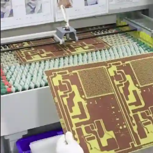
Sometimes, seeing beginners scribbling countless wires on generic boards makes me want to remind them to upgrade their thinking. Especially when dealing with high-frequency signals or high currents, the routing and layering directly affect the stability of the entire system. Last week, I helped a junior modify a robot’s main control board, which was a typical example. Originally, a double-sided board caused motor interference, but switching to a four-layer board with a separate power layer solved the problem. Layered design can effectively control electromagnetic compatibility (EMC). For example, sandwiching sensitive signal layers between power and ground layers acts like adding a shielding layer to signal lines. Impedance matching in high-frequency circuits also relies on precise layer stack-up structures, which are difficult to achieve with generic boards.
While prototyping costs are indeed much lower than before, the key is to understand your specific needs. Asking “What’s the cheapest PCB?” is problematic in itself. I prefer to first consider the actual application scenario of the circuit. For example, making a control board for underwater equipment requires waterproofing, and industrial environments necessitate enhanced heat dissipation—these details are often more important than price. Different surface treatments have their advantages and disadvantages; immersion gold is suitable for high-precision pads, while tin plating is cheaper but has slightly less flatness. Board material selection is also crucial; high-frequency circuits require low-loss Rogers materials, while flexible circuits require polyimide substrates.
Of course, not all projects require custom-made boards from scratch. For some simple prototype development, using off-the-shelf boards is more efficient—the key is to strike the right balance. After all, time is also a cost; blindly pursuing customization may be counterproductive. For example, when validating a sensor algorithm, a test environment can be set up in half an hour using an off-the-shelf Arduino expansion board, while a custom board takes at least a week from design to prototyping. This rapid iteration approach is particularly common in startup teams, who often employ a modular strategy—validating core functions with development boards and then integrating them into a custom PCB for mass production.
What fascinates me most is the feeling of seeing my designed circuit board perfectly integrated into the product; the seamless experience is like a tailor-made suit, making you feel incredibly confident. This sense of accomplishment is far stronger than simply buying off-the-shelf modules and assembling them, since every corner and every trace is meticulously planned according to actual needs. I remember once designing an irregularly shaped board for a mini drone; the circuitry between the battery compartment and the motor mount was like a maze, but hearing the “click” of the clips closing during final assembly was an indescribable pleasure.
Ultimately, custom PCBs are more like a design mindset; they force you to think about circuit layout from the perspective of the overall product. Once you develop this mindset, you’ll find that many seemingly unsolvable mechanical structural problems can actually be resolved through clever circuit board shape design. I’ve recently gained a deep understanding of this while working on wearable devices—when circuit boards can bend with fabric, the design space for the entire product suddenly becomes much more expansive. For example, the curved motherboard of a smart bracelet can perfectly fit the wristband, allowing motion sensors to collect data closer to the skin. This three-dimensional layout thinking has even given rise to 3D circuit board technology, allowing electronic components to be arranged in multi-dimensional spaces like building blocks.
Making circuit boards is quite interesting. Many people immediately think about saving money and time by choosing a ready-made PCB and making do—I used to do that too. It wasn’t until I was tinkering with a small smart home gadget that I realized the problem wasn’t so simple: the signal was constantly intermittent, it overheated to the point of burning my hand, and the battery life was less than half a day… Later, I understood: not all circuits can fit into the same board.
After that, I started to think about what custom PCBs really mean. It’s not just about changing the color or size—true customization starts with understanding what your product needs to do. For example, if your device needs to operate outdoors in windy and sunny conditions, the circuit board material must be heat- and moisture-resistant; for wearable devices, a flexible and lightweight design is more important than performance parameters.
A friend of mine previously made an outdoor sensor. Initially, to save time, he used ordinary FR4 board material. However, in the high temperatures of summer, data acquisition completely messed up. He later redesigned it, replacing the board material with a high-TG material and adding heat dissipation holes, and only then did it stabilize.
Sometimes I feel that custom PCB design is more like building with blocks, except you have to draw the shape of each block yourself. It doesn’t test how much you know about technical parameters, but whether you can truly understand where the product will be used and what problems it will encounter.
Recently, I’ve seen many newly established teams particularly fond of pursuing “one-step solutions,” trying to cram all functions into a single board. The result is often cost overruns and unstable performance. It’s better to first clarify the core requirements. For example, a simple temperature and humidity sensor really doesn’t need a six-layer board; a two-layer board with a reasonable layout is sufficient.
Ultimately, good circuit board design is not about piling on components, but about refining your understanding of the application scenario bit by bit. When you truly put yourself in the user’s shoes and think about how the board should work, those seemingly complex issues will become clear.
In the field of industrial automation, people often pay attention to AI
Ever wonder how your phone maintains a stable signal? It relies on
When selecting components for a security monitoring system, most attention goes to
- Experto en producción de lotes pequeños y medianos
- Fabricación de placas de circuito impreso de alta precisión y montaje automatizado
- Socio fiable para proyectos electrónicos OEM/ODM
Horario comercial: (de lunes a sábado) De 9:00 a 18:30