

Turnstile Access Control PCB: How Grounding, Power-Loss Release and Board Fabrication Decide Whether a Gate Survives 5 Million Cycles
How grounding, power-loss release hardware, and multilayer or HDI fabrication decide whether
A TPU PCB forces several conflicting physical limits onto one board: multi-order HDI density, heavy copper for hundreds of amps, 56Gbps-class high-speed links, and torus-style ICI interconnect that needs symmetric routing on every edge. Very few fabricators master all of these at once, and layer count is the least important metric. The most dependable approach is to evaluate ICI escape routing before HBM fan-out, consider splitting the design into a high-speed logic board and a heavy copper power board, ask every candidate supplier for cross-section reports of comparable boards, and screen for real production experience in combining thick copper with fine impedance-controlled traces rather than for headline specifications.
In recent years, more and more teams around me have been working on AI hardware. Everyone talks about chip architecture and compute figures, but when they actually start building the carrier board for an ASIC, they find that the bottleneck is often not the chip itself but the unremarkable printed circuit board underneath. We used to treat the PCB as a mindless wiring layer, until one project taught us a hard lesson.
It was a prototype board for a custom tensor compute unit, similar to a TPU in concept, except that the ASIC was entirely our own design. The chip had not even come back yet, and we had already stumbled on PCB resources. The requirement sounded straightforward: a 38-layer board mixing multi-order HDI with heavy copper zones for high current, while preserving signal integrity for several groups of high-speed buses. We approached several well-known multilayer PCB manufacturers. Most of them shook their heads as soon as they heard “38 layers,” or stretched the lead time to more than 22 weeks.
This made me realize that in a specialized accelerator field like ASICs, finding the right multilayer PCB supplier is not simply a matter of commercial procurement. It directly determines whether your chip can run in the real physical world. An ordinary server motherboard maker simply cannot handle this kind of board, because it has neither a mature production line for high-layer-count HDI nor a process reserve for heavy copper that carries concentrated high current. Later we talked to several manufacturers that specialize in HDI PCB. They claimed they could do third-order or even any-layer interconnect, but when we actually evaluated them, once they met our requirement of interleaving power layers with high-speed signal layers, many HDI PCB suppliers began to suggest simplifying the stackup, which amounts to making us sacrifice the design for the sake of their process capability.
The turning point came when we decided to prototype the power module and the main logic board separately. The main logic board focused on routing and high-speed processing, and we found a high speed PCB manufacturer that had long supplied backplanes for communications equipment. Its strength is not stacking layers but real experience in controlling dielectric loss and impedance consistency, which was critical for our 56Gbps chip-to-chip link. For the power daughter card we separately found a heavy copper PCB supplier that specializes in thick copper. Copper on the board went straight to 8 ounces, and the traces for several core power rails were as wide as a little finger. This division of labor sounds like a self-imposed compromise, but in retrospect it fits the real rhythm of ASIC development better. If the chip pinout changes, you only need to remake the power board, and the logic mainboard does not have to be torn up along with it.
Looking back now, no matter how elegant the internal interconnect architecture of a dedicated processor at the TPU level may be, it all has to be realized through the physical carrier of the PCB. Many hardware teams make one mistake when choosing PCB partners for an ASIC: they put blind faith in big-name multilayer PCB manufacturers and neglect to evaluate specific process strengths. For example, some factories are good at the miniature HDI boards used in mobile phones but are helpless with large, highly rigid, telecom-grade heavy copper boards; others advertise themselves as heavy copper PCB manufacturers but actually have no experience designing the heat dissipation path after multilayer lamination. The suppliers we eventually settled on are all small in scale but deeply specialized. The one that makes high-reliability boards above 30 layers makes only that kind of board, and the one that studies the thermal-electrical coordination of thick copper will even help you work out the transition from FR4 to ceramic-based material.
I am not telling this story to sell anxiety but to dispel a myth: when building an AI accelerator, do not focus only on the moment the chip taped out successfully. Real physical deployment begins the moment you can steadily obtain a TPU PCB that meets the design specification. Problems such as interlayer registration deviation, local overheating from uneven copper thickness, and high-speed eye closure can each drive you mad late in a project. The key to solving them is often not in your schematic but in which HDI PCB manufacturer and which heavy copper PCB supplier you choose to make the first prototype. We have paid for this lesson, so now, even if the stackup evaluation costs three more weeks, we will never over-compromise on the PCB. After all, for a board that must carry hundreds of amps of current while maintaining picosecond-level timing, the cost saved on paper is paid back double during debugging.
After dealing with AI accelerator hardware for several years, I have noticed a rather counterintuitive phenomenon: many teams designing TPU boards are not stuck on the chip itself but are driven to distraction by a PCB. It is quite unexpected, because normally everyone pours their energy into the silicon architecture, and only after the tape-out comes back do they find that the board carrying the chip has become the biggest headache. Especially when the HDI PCB manufacturer you choose cannot handle high density and heavy copper at the same time, the thermal performance and power integrity of the whole project turn into a mess.
Once, a team building a dedicated TPU came to us. Their board design was quite aggressive, with blind and buried vias packed densely under the chip and a required copper thickness of more than 6 ounces. When the first samples came back from the multilayer PCB supplier we were working with at that time, the copper foil bulged outright and the via continuity did not meet the standard. We then switched to an experienced heavy copper PCB manufacturer to remake it. They changed the lamination parameters and swapped the prepreg for a high-heat-resistance grade, which only barely brought down the unevenness. This made me realize that what a TPU demands of a PCB is not about adding more layers; it is about forcing several mutually conflicting physical limits together.
Many people like to compare a TPU board with a high-end GPU board and think both are high-layer-count designs, not very different. In reality, the fearsome interconnect requirements of a TPU push a multilayer PCB in a completely different direction. For example, the ultra-wide ICI interface between chips requires length matching of hundreds of differential pairs down to the picosecond level, so traces have to wind around and the stackup is forced to grow beyond 30 layers. On top of that, because the chip’s power density is absurdly high, currents on the board often reach hundreds of amps, and the thin copper foil of an ordinary high-speed board simply cannot carry it, so you must go to a heavy copper PCB supplier for silicon dioxide–based substrates or thick copper processes. A single board has both extreme high-speed signals and high-current power layers, and signal integrity and current-carrying capacity fight each other. An ordinary high speed PCB manufacturer has to think for a long time before taking such an order, for fear of damaging its own reputation.
What is worse, screening suppliers for this kind of board is especially exhausting. We previously evaluated several multilayer PCB manufacturers. Some are strong in high layer counts but cannot cope once embedded copper blocks or 10-ounce thick copper come in; some HDI PCB suppliers can approach third- and fourth-order blind vias but cannot reach the required loss grade in high-speed materials. Factories that can handle all these dimensions at once are very few, and the quote is often more than double that of an ordinary PCB with the same layer count. Once PTFE or ultra-low-loss materials are involved, the yields of drilling, desmear and plating drop alarmingly. These boards simply cannot be mass-produced at scale and can only go through small-batch special processing.
Looking back now, chips like the TPU have forcibly turned the PCB from a standardized carrier into a highly customized physical system. It is no longer as simple as “drawing out the copper lines”; it is about finding balance among materials, thermodynamics and electromagnetic fields. Whenever a new project starts, I remind the hardware team not to rush to fix the chip architecture before talking with PCB suppliers, because the option you think is safest may well be the yield hell of the board factory. After all, a board at this level is no longer a problem that money alone can solve. You have to spend time polishing the process details, and the chip datasheet will never tell you those things.
Recently a project building a TPU accelerator card completely changed my view of a badly underestimated part of board-level design. In the past, whenever people talked about TPUs, the topic always revolved around HBM, as if the PCB were finished once the fan-out of the HBM3e high-speed interfaces was routed. In fact, what really tends to drag the whole board into a dead end is the ICI interconnect. The TPU has a high proportion of on-chip SRAM, and its HBM interface is not as extremely wide as a GPU’s, which gives many people the illusion that they can free up more routing resources from the HBM side. The problem is that the number of ICI links is not small at all, and they are distributed along several edges of the chip. The signals must be both pulled inward toward the board and routed out to adjacent cards, so the physical directions are much more complicated than those of HBM.
Once you squeeze space in the order of “HBM first, ICI later,” the ICI escape channels are, in eight or nine cases out of ten, chopped into fragments. By then the delay skew of the differential pairs cannot be compensated, and the board-level bit error rate gets stuck and will not come down. After I fell into this trap, I became especially careful when choosing multilayer PCB makers. Not every multilayer PCB supplier can treat these two high-speed domains equally, especially factories that just stack up layers and claim HDI capability, which are exposed the moment they meet stacked vias or any-layer interconnect. A truly capable HDI PCB manufacturer will, from the very start, discuss with you how copper thickness and dielectric thickness can be made compatible, because the power of a single TPU chip can easily reach the kilowatt level, and the heavy copper used by the power delivery network and the high-density routing of the high-speed area are stacked on the same board. This tests a supplier’s real skill in lamination, drilling and etching control.
So when I look for a heavy copper PCB manufacturer now, I do not pay much attention to the maximum copper thickness they can do. Anyone can quote that number. What matters is the yield with which they make fine impedance traces on thick copper layers. If a large-area power island and dense high-speed differential pairs sit on the same layer or adjacent layers, a slight deviation in pattern plating makes the line width drift, and the high-speed side is simply ruined. Only a factory that can resolve this contradiction is a truly experienced high speed PCB manufacturer. This kind of capability is often not written in the specification sheet. You have to go and see their production line in person, or ask their NPI team to talk through cross-section reports from similar boards they have made before.
In addition, many people stake the success or failure of a TPU PCB entirely on stackup simulation, but no matter how accurate the simulation model is, it cannot withstand the batch-to-batch fluctuation of dielectric thickness in processing. Especially when a single multilayer board must take care of both the short-distance fan-out of HBM and the long-distance reach of ICI, the stability of material Dk and the flat-weave structure of the glass cloth matter more than anything. When I talk with HDI PCB suppliers now, I ask in advance for the batch consistency data from the laminate supplier, and then require the board factory to take actual cross-sections of every batch after lamination, rather than looking only at the TDR curve. If you put in this effort early, you will not have to chase signal integrity problems every day during later system bring-up.
On the TPU road ahead, as the inter-TPU interconnect rate doubles again, signal integrity and board-level loss on the ICI side will push more people to re-examine their PCB resource allocation strategy. If you still hold on to the old HBM-first mindset, the board either cannot be routed or its cost goes out of control. Finding earlier a factory that understands both heavy copper and fine HDI will give you much more room in the design, and this is far more important than haggling over price at the last minute.
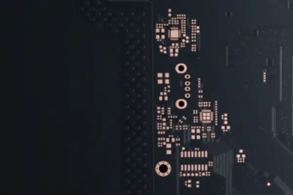
The biggest lesson from the several custom TPU boards I have handled is this: do not stare at the eye diagram of the differential lines all day. What really kills a project is often the physical conflict between the power layers and the ICI torus routing. The core current of one TPU easily surges to hundreds of amps. At that point, when you take a sample from an ordinary multilayer PCB supplier and the copper thickness goes above 3oz, the layer-to-layer alignment starts to drift, and with slight process deviations in the thermal vias and the large inner-layer copper areas, the whole board is scrapped. After being burned twice, I started to specifically screen heavy copper PCB manufacturers that had truly built thick copper boards, rather than workshops that only stack multilayer boards for high-speed routing.
The torment that torus interconnect inflicts on board-level layout is far more perverse than imagined. The ICI links must lay out several groups of high-density connectors along the board edge, and the trace length in every direction must be held nearly identical; a difference of a dozen mil throws timing into chaos. But once a heavy copper power plane is spread out, the escape space left for these high-speed differential lines is squeezed into narrow slits. Many HDI PCB manufacturers get a headache the moment they see this stackup, because the traditional 2+N+2 structure simply cannot cope, and when it is forced in, via stubs are hard to control and the return loss is miserable. I once found a manufacturer that mainly positions itself as a high speed PCB manufacturer. Its final solution was to use 3+N+3 plus local buried vias, completely isolating the thick copper area in a power sub-stackup, which only barely stabilized the reference plane of the ICI signal layers, at the price of directly doubling the cost.
So the layer count that people in the field like to discuss is actually not very meaningful for a TPU. Even if you stack up to 30 layers, if the slack of the torus topology and the heat dissipation of the thick copper are not handled well, that TPU PCB is a money-burning black hole. When choosing a heavy copper PCB supplier or HDI PCB supplier now, the first thing I ask is whether they have handled projects combining torus architecture with ultra-thick copper. Without that experience, I dare not touch them, however low the quote. In the end, a cloud accelerator card is not about who can get the traces routed through, but about who can truly fit the physical dimension of ICI and the electro-thermal stress into the same board.
In my years working with custom accelerator cards, one realization has grown stronger: a TPU PCB is not what ordinary players imagine, a matter of “pressing a few layers of board together.” Many people think that stacking layers up to thirty or forty and switching to top-grade materials settles everything. In fact, in the field of compute boards, layer count is the least important metric. What really takes skill is the tug-of-war between copper thickness and fine lines.
Some time ago I chatted with a friend who runs a heavy copper PCB manufacturer. He complained that the inquiries he receives now often ask for 10oz copper with 3mil differential lines routed underneath. Putting these two requirements on one board is, process-wise, like the left and right hands fighting each other. Thick copper means that when the etchant bites into the copper foil, the side etching is much greater than with thin copper. A designed line width of 3mil may end up at 2.5mil or even thinner, and the impedance drifts away directly. And anyone who works on high-speed digital circuits knows that once impedance is off, the eye closes immediately, and the link budget has only that little margin and cannot withstand this kind of tossing about.
This is also why, when choosing a multilayer PCB supplier, I never look at the theoretical layer count and minimum line width that they boast on their website. Instead I ask directly: “Has your factory actually produced orders combining copper above 10oz with fine lines below 3mil?” The answer to this question can screen out about ninety percent of candidates. Many factories that label themselves as multilayer PCB manufacturers can actually only make thin-copper HDI or only thick-copper power boards, and their process experience in the two directions is completely separated. A TPU-class board, however, interweaves the power layers and signal layers, so you must run both processes smoothly on the same production line.
I have seen a case in which a fairly well-known HDI PCB supplier, while making prototypes, over-etched the window openings of the thick inner-layer copper, causing micro open circuits in the copper of several dozen VRM modules. After power-up, several modules lost power directly, the PDN impedance surged, and the chip shut down instantly. The investigation later showed that the spray-pressure parameters of that etching machine were simply unsuitable for thick copper. This kind of pit is hard to notice before you step in it, but once you do, the project stalls.
As for the high-speed signals, many high speed PCB manufacturers now care only about the material Df and often ignore the effect of copper foil roughness on insertion loss. On a TPU board the dielectric of the signal layers is as thin as paper, and once the copper is thick, the resin flow during lamination affects dielectric uniformity. This is another deadly contradiction. So it is useless to find just a factory that can laminate ultra-low-loss materials; you also have to see whether it knows how to balance stress between thin dielectric and thick copper.
Back to etching: I think it is the part of all these manufacturing steps that outsiders understand least. Etching is not a single bite that removes the excess copper; it is a dynamic game among time, temperature and chemical concentration, and the pattern density differs enormously across different regions of the board, so it is hard to take care of uniformity with a single parameter. Some heavy copper PCB suppliers have now begun to use pulse etching and multi-step etching for fine control, and yields have gone up, but the capacity is terrible. A team that can steadily mass-produce TPU-class carrier boards must have spent several years grinding in these process windows.
So my view is simple: the essence of a TPU PCB is a pile of mutually contradictory design requirements forced into reconciliation on a physical carrier. Only factories that have mastered all three dimensions of HDI, thick copper and high speed dare to say they truly understand this.
After making boards for so many years, I have slowly come to understand one thing: the routing of power on a board has never been something solved by one or two thick traces. Especially when a single chip swallows hundreds of amps, you cannot expect to place one huge voltage regulator module at the board edge, pour copper as flat as an iron plate, and consider everything settled. If you actually do that, voltage drop and heat accumulation will pop up in places you never expected and make trouble.
So when I look at a TPU PCB solution now, I pay more attention to approaches that “crumble” the power modules and tuck them around the chip. It is not simply a matter of making the VRM smaller; it is about making every small portion of power like the chip’s own breathing organ, sitting right under or beside the BGA, so that the current path is short enough for parasitic inductance to be almost negligible. At that point you find that the role of thick copper foil is not as shallow as merely “lowering resistance.” It creates a low-thermal-resistance heat-dissipation base for those distributed modules and, at the same time, swallows up the lag in transient response. I have seen a friend who runs a heavy copper PCB manufacturer make inner-layer copper up to 12oz and stack it beneath the modules, and the impedance curve of the entire PDN, from low frequency to high frequency, was as smooth as if it had been ironed. But note that suppliers of such boards are not easy to find. Many multilayer PCB suppliers, as soon as they hear that you want to stack thick copper, immediately say that interlayer alignment will shift and impedance control cannot be fine. But if you go to a manufacturer that specializes as an HDI PCB supplier, they may in turn be unfamiliar with thick copper processes, and laser drilling tends to burn the holes. Later I found a factory that can make multilayer boards of more than 20 layers and also dares to laminate 10oz copper on power layers. It also runs a high speed PCB manufacturer business and has a good feel for stackup structure, so communication was much smoother. Come to think of it, this was also a lesson: do not expect one manufacturer to do everything. You have to figure out whether it is an HDI PCB manufacturer skilled at fine lines or a multilayer PCB manufacturer able to handle heavy copper, because the pain points of the two processes are completely different.
In addition, when many people talk about impedance control, they stare at capacitor selection and placement, but I think the more fundamental thing is the combined effect of the module and the PCB. You spend a lot of money on ultra-low-ESR MLCCs, but if the parasitic inductance of the copper loop in the stackup is not suppressed, it oscillates anyway. From my own experience, first make the PCB path between the VRM module and the chip short enough and “fat” enough, and then the lower bound of the impedance is actually determined jointly by the module’s own switching frequency and the PCB’s interlayer capacitance. This is easy to say, but when drawing the board there are always many trade-offs between layout and process, and that is the most tormenting and also the most interesting part.
A previous TPU accelerator card project gave me quite a different feeling about PCB prototyping. The whole team was staring at the chip’s compute density and overlooked whether the board carrying it could actually hold up. A TPU’s heating pattern is very different from a GPU’s. It is not spread evenly; the hot spots concentrate like sunlight focused by a magnifying glass, and that is when the directories of manufacturers labeled “heavy copper PCB manufacturer” become especially critical.
I have gone through the process capability sheets of several multilayer PCB suppliers and found that very few actually dare to go above 10 ounces of thick copper. Many people think thick copper just lets current flow more freely, but the pits I fell into later taught me that its real strength is pulling heat sideways like a vapor chamber. If a thick copper layer does not help spread the temperature near the VRM, local spots can soar above a hundred degrees, and the chip, even only a few millimeters away, suffers along with it. But this is easily overlooked at the quotation stage. Everyone only asks “can you make a 4-layer board” and “what is the impedance control accuracy,” and never mentions the thermal conductivity parameters of thick copper. I have since learned my lesson and ask the heavy copper PCB supplier directly whether they can provide cross-section reports after resin filling, to check for residual bubbles in the grooves. Bubbles slowly grow under thermal cycling, and after a year or so they start to cause random connection drops, and that kind of debugging is the most painful.
The routing density on a TPU board is another extreme. The ICI links need more differential pairs than an ordinary GPU board by a good margin, and the length-matching requirements are almost harsh. I once ran into a case where, in order to let high-speed signals run straight from the chip edge to the connector, a large patch of decoupling capacitors had to be squeezed onto the back side, and then the back side collided with the heat-dissipation base of the power modules. Only then did I realize that finding an HDI PCB supplier cannot be just about how many orders of laser vias it can stack; you must ask clearly whether it can coordinate stacked vias, via-in-pad and thick copper. Some multilayer PCB manufacturers optimize their processes separately: an HDI line used to phone boards starts to complain as soon as it meets 2mm-thick copper, saying that it cannot control the etch factor. But a TPU board happens to be exactly this kind of hybrid: high-density interconnect under the chip, turning outward into thick high-current copper layers, and if the transition in between is even slightly abrupt, the signal eye closes.
I remember once chatting with an engineer at a high speed PCB manufacturer. He showed me a cross-section from a prototype board in which the copper thickness on the core was uneven, differing by a few microns, and the impedance curve measured by TDR fluctuated so much that it was unreadable. He said that the dielectric thickness of high-speed laminates is already very thin, and when the fluctuation of copper thickness takes a large proportion of it, impedance gets completely out of control. Later we switched to a multilayer PCB manufacturer that came from chip test-board manufacturing. It still used a modified semi-additive process, pulling line-width accuracy to within ±10%, and only then was the eye reopened. This experience made me give up completely on measuring a TPU PCB by the standards of an ordinary server board. It is more like forcibly kneading together the mutually conflicting needs of HDI, high speed, thick copper and large size, and a factory without sufficient experience simply cannot tune the parameters flat.
The ICI escape routing around the chip is also a headache. I once naively thought BGA fan-out was standard work, only to find that the TPU bump map is arranged especially densely, with some power and ground pins sandwiched between high-speed signals. If the power loop is not planned in advance, you cannot even pull the pads out of the capacitors later. Later we were forced to have the layout engineer connect directly with the front-end engineer at the board factory during the layout stage, turning the stackup structure, copper thickness distribution and solder-mask openings into one linked parameter table. Many HDI PCB manufacturers can actually provide this kind of co-design service; we just did not ask at the beginning, and only found after finishing the drawing on our own that it could not be built. Thinking back now, if we had placed the capability list of the heavy copper PCB manufacturer side by side with the process capabilities of the HDI PCB supplier early on, we could have saved at least two revisions.
In the end, this TPU board taught me one thing: do not treat the PCB as an accessory of the chip. It determines how current runs, how heat dissipates and how signals shake hands, and even directly frames how the liquid-cooled cold plate of the whole machine should be designed.
A few years ago, when I was helping a friend debug a TPU accelerator card, I noticed a particularly glaring problem. A dozen minutes after the board started running, the compute began to jitter, and the logs were full of throttling records. When I opened up the thermal imager, the chip surface temperature was held down by the heat sink, but several areas on the back of the PCB were outrageously hot, with the heat stuck inside and unable to get out. At that moment I suddenly understood that many people put all their energy into choosing how big a heat sink to use, when the real choke point is the thermal channel design of the PCB itself.
During that period I went through the process capabilities of quite a few board factories and went back and forth haggling with the technical salespeople of several multilayer board manufacturers. For a chip like the TPU at several hundred watts, the solution most conventional factories offered was standard thermal vias with copper filling, which sounds fine. But when I put forward the via density requirement, many suppliers began to hem and haw, saying the process was hard and yield would drop. In particular, requiring via-in-pad with deep copper filling, with uniformity across the whole array, no voids, and the ability to withstand the subsequent lamination steps of a multilayer HDI board, is a much higher bar than imagined. I found that if you casually throw such an order to an HDI PCB manufacturer unfamiliar with high-density thermal management, what comes back is often reduced via density or incomplete filling, and the thermal resistance test fails outright.
Later I switched to a factory that specialized in high-speed, high-layer-count boards. Their suggestion was to connect the thermal via area with the thick inner-layer copper and use multiple copper foil layers to share the vertical heat. This solution brought another problem: the inner-layer routing space was heavily squeezed. The high-speed signals around the TPU were already dense, and squeezing differential lines out one by one inside the thermal via array was like embroidering on a heat sink. That is when the stackup design level of the HDI board supplier is really tested: whether it can let the thermal vias run through the copper layers as much as possible while preserving signal integrity. We later adopted a stepped via layout, sacrificing two signal layers in exchange for a more direct thermal conduction path, and the measured junction temperature dropped by nearly eight degrees.
Another point that is easily overlooked is the mechanical constraint brought by the cold plate. In an earlier project, a large cold plate covered a whole row of TPUs and VRM modules, and we thought that handing all the heat to liquid cooling settled everything, but problems kept coming up during assembly. Uneven clamping pressure of the cold plate caused slight bending of the PCB in the BGA area, and after running for a long time the solder joints occasionally developed micro-cracks. Later, in the design review, I insisted that the structural engineers add stiffening ribs and limit slots under the cold plate, and had the multilayer board supplier adjust the board thickness tolerance and solder-mask flatness, and only then was the stress problem barely under control. Thinking back, for this kind of board-level thermal design, the PCB manufacturer and the thermal module vendor must be brought together from the very beginning to work on the design; otherwise, if any party takes matters into its own hands, it is reliability that ends up paying.
Now when I choose suppliers, I am particularly strict about some key parameters. For example, a heavy copper PCB must have sufficient copper thickness, but etching precision cannot be given up for the sake of heat dissipation, since outer-layer copper on high-speed signals that is too thick affects impedance. A good heavy copper PCB manufacturer knows how to isolate the heat-dissipation layers from the signal layers, using thin copper for signals and thick copper for current and heat, and genuinely pushes the process parameters into place. Suppliers who beat their chests and say there is no problem at every turn but cannot even produce a thermal resistance test report are basically skipped outright.
So in the end, the thermal design of a TPU PCB is not an issue of a single via process. It is closely tied to the HDI stackup, the cold plate architecture, the board thickness, and even the supplier’s understanding of the actual physical boundaries. Moving heat out is only the first step. Whether it can be moved out stably, without affecting signals or hurting solder joints, is where the real value lies.
The biggest takeaway from building large liquid-cooled accelerator cards of this kind is this: never treat the PCB and the cold plate as two independent things. In the past, we were used to finishing the board and throwing it to the structural team, who would then cut a cold plate and press it on, and after several rounds of back-and-forth changes, either the mounting holes did not line up or the clamping stress concentrated at a few BGA corners, and after a month of running the solder joints began to micro-crack. Now, when working on boards at TPU-class power, I pull in the cold plate designers from the beginning to decide the stackup and the stiffening rib positions together, especially for boards above 30 layers using an ELIC structure, where the HDI PCB manufacturer you choose almost determines how much rigidity you can achieve. Some factories can embed shaped copper blocks, while others can only build thickness by stacking copper foil layers, and the deformation during cold plate clamping is completely different.
When talking to a multilayer PCB manufacturer about this kind of project, do not start by asking how many layers they can do and what the line width and spacing are; anyone will beat their chest on that. Ask directly: have you made a board with local 10oz heavy copper that also carries 112Gbps high-speed lines? If the other party is a reliable heavy copper PCB manufacturer, they will talk with you about copper thickness uniformity after lamination and the Z-axis expansion coefficient after resin via filling, not just quote a price. I got burned before. A sample from one heavy copper PCB supplier looked sufficient in copper thickness alone, but once high current ran, the CTE mismatch between the inner copper and the base material cracked the microvias, and the investigation finally showed that their lamination process had not been controlled below the Tg temperature. For this kind of board, thermal simulation is not finished after one run. You have to correlate the cold plate’s actual thermal resistance, the coolant channel distribution and the temperature drift of the laminate Dk; otherwise the signal eye looks fine at room temperature, but once the full-load temperature rises to 85 degrees, the skew of the ICI traces goes directly beyond spec.
The interface between the cold plate and the PCB also hides an easily overlooked pit: condensation. We added a leak detection tray on top of the rack, which is already a system-level safety backstop, but the protective coating of the board itself is the first line of defense. Many people feel that applying conformal coating settles it, without considering that the micro-gaps in the contact area between the cold plate and the PCB form an active “breathing effect” during hot and cold cycling, slowly drawing moisture in. Later I had the multilayer PCB supplier add a ring of sealing copper around the edge of the high-voltage area and added solder-mask-defined openings on the corresponding layers, and only then did it finally quiet down. When looking for a supplier for this kind of board, you cannot look only at whether it is an HDI PCB supplier; you must also see whether it has remediation experience coupled with cold plates. Otherwise, after three rounds of trouble at the prototype stage, the whole project schedule is used up.
In my two years in AI hardware, my biggest takeaway is: do not trust the parameters on supplier websites too much. For those manufacturers that mark “can make 30-layer boards” at every turn, when you really send over the drawings of a TPU PCB, eight out of ten go silent.
Last year, while choosing a board for an inference accelerator card, we first approached a multilayer board manufacturer that had made many consumer electronics boards, and the salesperson patted his chest and said they could do multilayer boards with their eyes closed. But when they heard that the power layer needed 5-ounce copper stacked together with a 3mil thin dielectric, the engineer stopped responding on the spot. Later I got smarter and specifically looked for factories with heavy copper PCB manufacturing experience, but this type of factory in turn easily trips up on fine lines. Once I visited a production line: they were fierce at etching heavy copper, but once the chemical hit, the 30/30 micron lines were side-etched and deformed outright, and the impedance was off beyond measure. In the end, a factory that can do thick copper cannot necessarily hold fine lines, and conversely, one that can control fine etching is at a loss when it goes up to heavy copper.
Microvias are another pit. Quite a few manufacturers that call themselves HDI, upon hearing that we wanted 75-micron holes connecting to large inner-layer pads, said an extra charge could handle it, but the real lifeline is the actual registration capability. We tried once: the board reached twenty-something layers, the layer offsets accumulated, and the connection area between the bottom of the hole and the pad shrank by a large chunk, and problems appeared as soon as thermal cycling ran. Later I focused on those high-layer-count board suppliers with real X-ray alignment production lines. I did not look at what their quotation sheet said but asked the on-site engineers directly: when was the last time you built a board of more than 30 layers containing microvia structures, and what was the yield?
The consensus in the circle is now becoming clearer: factories that can combine these processes are basically no longer simple multilayer board suppliers. They are either long-term makers of high-speed PCBs with a foundation in impedance and interlayer structure, or factories dedicated to heavy copper that spent heavily to upgrade pattern transfer and lamination equipment. In the end I handed my batch of boards to a high-layer-count factory that had built countless AI server boards and left it to carry the load. Of course, the price was also a large chunk higher than for ordinary boards. But that is how this industry is. If you want to stuff 40 layers, 10-ounce copper and 75-micron holes all onto one board and still expect it not to collapse while running, there are very few heavy copper PCB suppliers who can take it on. Spending more money is better than overturning after mass production.
In the AI chip race of recent years, building GPU cards and building TPU cards are almost two completely different ways of living. When I first came into contact with this kind of project I also thought it was nothing more than stacking a few more layers, and only when I actually got my hands on it did I realize it was not like that at all.
There seem to be quite a lot of factories on the market that can seriously qualify as high-end multilayer PCB manufacturers, but once a board goes beyond twenty layers and the dielectric constant must also be pinned in a low-loss range, the list shrinks immediately to something you can count on one hand. When we were choosing a substrate for a self-developed TPU, material selection alone took us almost a month. The GPU side is easy: the design template is relatively fixed, and the broad framework of high-speed routing is already covered for you in NVIDIA’s reference design, so you simply find a qualified high speed PCB manufacturer and push through step by step. But the TPU is different. The interconnect between chips has to be carried by board-level routing, link budgets are calculated by hand one at a time, and ordinary M6-grade materials simply cannot hold signal integrity, which forces you toward M8 or even higher-grade hybrid-lamination solutions.
More troublesome is power. Once the TPU core runs, the current is outrageously large, and if the copper is not thick enough the voltage drop blows up immediately. We had no choice but to find factories that could act as heavy copper PCB manufacturers, while also requiring them to retain high-density routing capability, which is equivalent to asking them to knead thick copper processes and fine lines into the same board. Later I talked with a veteran multilayer PCB supplier, who said frankly that they are also afraid to take this kind of order, that yield dropping to sixty or seventy percent is quite normal, and that the quote naturally flies up. Heavy copper PCB suppliers that can do this while also stacking any-layer HDI are really very few now.
It is not only a matter of layer count and copper thickness; package density also turns the soldering step into a long war of patching and repairing. The TPU’s BGA itself is large and has heavy thermal mass, and when the ordinary reflow profile is raised, after the solder melts the internal bubbles simply cannot escape. When we trial-built the first batch, the void rate we saw under X-ray made our blood pressure spike, and when we took it to the chip vendor for a reliability check, they sent it straight back. Afterward we forced the assembly house to redesign the stencil apertures, stretch the soak zone out entirely, and add nitrogen protection, and only then did we barely bring it into an acceptable range. That was when I truly realized that finding an HDI PCB manufacturer is not just about how deep a microvia it can make; you also have to see whether it has the ability to help you complete a full tuning of soldering parameters. Especially for a TPU PCB carrying a chip that draws dozens of watts at a time, any defect in the heat dissipation path will be amplified into a batch-level accident after mass production.
My personal experience is that a large part of the burden on a GPU card is shared out by proprietary interconnect protocols, so the pressure on the PCB is relatively mild, and picking a reliable multilayer PCB manufacturer and a qualified HDI PCB supplier basically gets it running. With a TPU PCB, you are essentially using the board material to make up for the tightly coupled capability that the chip architecture lacks, so the layer count, material grade, copper thickness and blind via structure are all pushed to the limit, and a cost several times that of a GPU solution is not surprising at all. When I talk requirements now, my first sentence is usually: “Have you ever made a board of more than thirty layers, with mixed-lamination PTFE, thick copper, and a BGA pitch below 0.8 millimeters?” An HDI PCB supplier that can answer is worth sitting down with.
In my two years of TPU design, my biggest feeling is that PCB work is not at all as simple as finishing the schematic and handing it to the board factory. Many times we thought we had found a multilayer PCB supplier, told them the layer count and the line width and spacing, and the rest was just waiting for the board to come back, but only when the HBM routing began did we realize how twisted this thing is. The 0.4mm pitch of the HBM interface forces you to use high-order HDI, and if you go through HDI PCB manufacturers that can do via-in-pad at this precision one by one, you will find that each one’s definition of yield differs by far more than a little. I used to think thick copper was only a concern for high-current power boards, and later I was severely educated by the distributed layout of VRMs: with more than 20 VRMs spread over one board, the thermal density looks spread out, but PDN impedance control immediately becomes a disaster, and if the thick copper area is slightly insufficient, the dynamic voltage drop goes straight off the chart. In that phase I tried almost all the manufacturers on the market that claimed they could make heavy copper PCBs, and found that the heavy copper PCB suppliers who dared to guarantee results were basically bragging. What they were used to making were crude power electronics boards, and they completely failed to understand the perverse requirements that high-speed signals place on copper thickness uniformity and etching precision.
What really stopped my losses was a high speed PCB manufacturer that does little advertising. They took a different approach: they did not rush to route, but spent three days going through the stackup with me again, completely separating the HBM differential pairs and the ICI torus traces that had been crammed into the same high-speed layer and giving each an independent reference plane. This move looked clumsy, but it instantly solved the signal integrity problem that had troubled me for several months. Only then did I understand that when looking for an HDI PCB supplier, you cannot just stare at how many orders of laser drilling are in their equipment list; you should also talk more about whether their engineering team has handled scenarios like the TPU, which carries both a large BGA and ultra-dense HBM. After all, the trouble of a TPU PCB is largely a pincer attack from both sides: on one side, the ICI links spread toward multiple board edges, with a balance of trace length and loss that is demanding to an almost perverse degree; on the other, HBM crowds along the package edge, where, if the 55μm line width and spacing is not matched with a via-in-pad process, yield in mass production can make you doubt life itself.
Later I also compared notes with a friend who works on edge inference. He used an NPU in a 35mm package and likewise stumbled on BGA voids and DDR5 eye collapse. A design with a 10-layer HDI board and 0.1mm laser microvias sounds uncomplicated, but if solder paste filling on the production line is slightly inadequate, voids appear in patches under the BGA. So now every time I choose a multilayer PCB manufacturer for a new project, I directly ask them to provide X-ray and cross-section reports for BGAs of similar size. Do not talk to me about process specifications; I only look at actual data.
When I used to do hardware, the place where we most often stumbled was not the high-speed signal routing but the carrier boards of the power modules. Sounds a bit unexpected, right? When a TPU system runs at full load, dozens of DC conversion modules crowd around the board and the thermal density is astonishing. At that point you will find that the performance ceiling of a TPU PCB is not entirely in the dozens of HDI layers under the main chip; more often it is held back by the process capability of the multilayer PCB supplier on the power path.
I have handled a failure case: a cloud TPU test board whose heavy copper area, because the lamination structure was not controlled well, had a Z-axis expansion coefficient mismatched with the HDI area, and began to delaminate after less than two months of thermal cycling. That multilayer PCB manufacturer claimed it could do 10oz copper thickness, but on a large-format, high-layer-count hybrid board, the uniformity of thick copper and inner-layer fine lines fell far short of engineering requirements. This completely changed how I evaluate HDI PCB suppliers. I no longer look at how many layers they can make or how fine the lines are; I go to the factory and camp out to see how they handle the stackup matching of the thick copper power layers and the high-density interconnect layers. This is where the real threshold lies.
The requirements a power module places on the PCB go in a completely different direction from those of the signal area. The signal area pursues low loss and impedance consistency, and a high speed PCB manufacturer has its own material library and back-drilling experience. But for power modules, a heavy copper PCB supplier must master current density distribution, thermal channel design and the thickness control of prepreg resin fill. It is hard for one factory to reach a high level in both. So later, when choosing partners for TPU projects, I deliberately separate the mainboard and the power carrier board, letting the HDI PCB manufacturer that makes the TPU PCB mainboard focus on fine dense lines, and handing the power modules to a heavy copper PCB manufacturer that specializes in gnawing on thick copper. It sounds like extra management trouble, but the first-pass yield actually more than doubled.
Many people think that outsourcing the power module PCB to a factory that makes ordinary multilayer boards will do, since it is only a few layers and the traces are coarse anyway. This thinking does great harm. The line-edge verticality of a thick copper board after etching, the reliability of solder mask via plugging, and the effect of copper surface roughness on thermal conduction at the soldering interface cannot be controlled without sufficient mass production experience. I have seen a module whose junction temperature after assembly was nearly 15 degrees higher than simulation because of improper surface treatment of the thick copper, which forced the system straight into throttling. And these details cannot be seen at all during the initial supplier screening from a drawing and a specification sheet. You have to go to the production line to see, and ask whom they recently supplied with similar power module boards and how long those have run under actual conditions. A supply chain is, in the end, the transmission of experience, not the copying of parameters.
Many people building accelerator cards habitually apply the GPU playbook to the TPU, but they are not the same thing at all. The deadliest thing about a TPU PCB is that it forces you to handle two mutually conflicting tasks on the same board: on one side, dozens of differential pairs with extremely low loss; on the other, power layers whose copper thickness easily reaches four or even six ounces, otherwise the transient current of several dozen amps from the VRMs simply cannot be carried. The several multilayer PCB manufacturers I have dealt with put a “risk surcharge” on the quotation as soon as you say you need a board of more than thirty layers mixing heavy copper and high-speed layers, and that tells you how awkward the supply chain is. GPU cards are usually twenty-something layers, and M6-grade materials can hold; but the TPU is different. ICI interconnect requires routing out of all four sides, and the topology forces you to do symmetric routing, which pins down the capability requirement for the HDI PCB manufacturer very tightly: you must not only be able to do high-density interconnect but also have experience with large-format heavy copper boards, otherwise the board skews once it runs and is scrapped.
Many people think that finding a heavy copper PCB supplier to take care of the power layers, then a high speed PCB manufacturer to take care of the signal layers, and putting them together will do. It is not that logic at all. In real mass production, if the resin flow control during multilayer lamination and the Z-axis expansion matching are not tuned well, the impedance of the high-speed channels drifts into a mess. I have seen a project where the VRM distribution was not aligned with the thermal design of the cold plate, causing local heat accumulation in the heavy copper area and directly closing the eye of the DDR5 channel, and it took replacing two multilayer PCB suppliers to barely suppress it. So the supplier you look for must be one that, within a single factory, can connect the thick copper etching of a heavy copper PCB manufacturer with the laser drilling and via-fill plating of an HDI PCB supplier. Otherwise, after one transfer in between, neither yield nor consistency can be guaranteed.
The GPU ecosystem is already very mature, and if you want to pick a supplier for GPU cards there is quite a lot of choice. But on the TPU side, the manufacturers that can cover, all in one, lamination accuracy for multilayer boards of more than thirty layers, heat dissipation of heavy copper power layers, and high-density interconnect laser via processes can be counted on your fingers. So every time someone asks me for selection advice, I say only one sentence: do not just look at BOM cost first; go to the supplier’s production line and take a look at their press and acid etching line, and see whether they can steadily run copper thickness of more than four ounces while holding line-width tolerance. That is more useful than any specification sheet.
After working on several TPU solutions, I increasingly feel that many people’s judgment of a board factory’s capability is still stuck on the very shallow metric of “how many layers it can make.” Pick any multilayer PCB supplier and they will beat their chests and say thirty layers is no difficulty, but the moment you touch the place where heavy copper and fine lines collide head-on, they start to hem and haw. This is not to say they are unprofessional; it is that a TPU PCB really is a bit cross-disciplinary. It requires one supplier to fuse high-speed routing, heavy copper current carrying and thermal channels onto a single board, while most manufacturers actually excel in only one or two of them.
The deepest pit I fell into was sending the mainboard of a TPU to an HDI PCB manufacturer with a good reputation, thinking that since it could do third- and fourth-order laser holes, high-speed differential control should be no problem. When the board came back and the components were mounted, the test showed an outrageous packet loss rate on the ICI channels, and our time was nearly all consumed hunting for signal integrity problems. In the end the cross-sections showed that the microstrip lines near the 10oz heavy copper layers had serious side etching, with line-width deviation far beyond the process window the factory had promised. That factory was indeed a qualified high speed PCB manufacturer, but it had never done real mass-production run-in on etching compensation for heavy copper and fine lines. After this, I completely abandoned the habit of reading the datasheet first and then choosing a factory. Now when I talk to a supplier, I always first ask whether they have real orders for AI server boards, especially projects with a Tensor Processor Unit and heavy copper power layers.
I have had similar experiences with thermal design. Many designers optimize the cold plate thermal resistance as low as it can go, and the simulation looks beautiful, but when the whole board comes back and is pressure-tested, the chip warps diagonally, and the thermal via stress in the neighboring VRM area is so large that it cracks the hole walls. Only after I talked to a technician at a dedicated heavy copper PCB manufacturer did I learn that the copper in the thick copper layer, while subjected to the cold plate mounting pressure, concentrates stress onto the hole walls through Z-direction expansion. If that moment is not balanced by the base material and the lamination structure, however good your thermal design is, it will be eaten by mechanical deformation. So now when I evaluate a board factory, I require them to provide actual-assembly torque distribution curves and batch stress test records, and this detail is often far more reliable than which certifications a supplier verbally promises.
In the library-building stage, many people tend to overlook one point: the ICI escape method is directly tied to the board stackup strategy. A TPU’s ICI is not a matter of just pulling a few groups of differential pairs. It naturally requires multi-directional symmetric routing, and the fan-out area heavily overlaps the routing beneath the HBM, forcing you to repeatedly splice multilayer fine lines and thick copper planes in limited space. This requires that the multilayer PCB manufacturer you choose be more than a factory that stacks and laminates; it must understand how the return path of high-speed signals stays continuous in heavy copper areas. After I finished my current project and cycled through suppliers, the one I ended up cooperating with long term was not the one with the loudest voice at the beginning but a mid-sized HDI PCB supplier with mass-production records in both heavy copper and HDI. Its inner-layer heavy copper can be filled with resin without voids, and the roundness of the hole shape after laser drilling is also well maintained, which is much stronger than getting a technical parameter sheet that looks perfect.
Thinking back, selecting a TPU PCB is far from comparing a pile of process data. You must recognize that it is essentially several mutually conflicting process limits forcibly pinched onto one carrier, and if any one dimension is off, the whole board is scrapped. If you also plan to push this kind of board later, I suggest not staring only at layer count and line width and spacing, but spending more time examining the supplier’s actual cases in three areas: copper thickness step handling, cold plate assembly and high-speed signal compensation. If a heavy copper PCB supplier can analyze side-etching data from cross-section photos in more detail than you can, then this is a collaboration worth pursuing.
In my years building AI accelerator boards, my biggest takeaway is: never think that for a multilayer board any similar factory will do. A TPU PCB, once it goes into volume, is completely different from hand-soldering a few samples in the lab. I stumbled right at the beginning of my career. Back then, to save trouble, I threw all the high-speed signals and the power section to an HDI PCB manufacturer that claimed it could do anything, and when the boards came back, the 10oz copper areas had blistered copper, and the 50-micron fine lines on thick copper blurred into a mess and were unusable. The other party explained that the heavy copper etching process was incompatible with HDI laser drilling, yet when taking the order they patted their chests and said there was no problem. Since then I have learned: the heavy copper power part and the signal layers must be managed separately.
In this industry, factories that can handle both high layer counts and thick copper can be counted on one hand. Later I split the power layers out and found a factory that specializes as a heavy copper PCB manufacturer. It could do 10oz or even thicker, but line accuracy was only so-so, and 50/50μm line width and spacing was out of the question. For the signal layers, I found another high-density-interconnect HDI PCB supplier, whose laser blind vias could reach 75 microns, with the dielectric thickness pressed to 60 microns and a fairly stable yield. Putting the two sides together, I was in effect shouldering the role of the multilayer PCB supplier myself. It is troublesome, but quality is at least controllable. The price is a longer delivery cycle and a somewhat higher cost, but compared with boards being scrapped and dragging the project down, the money is worth spending.
Many people ask me why I do not just find one factory that can do everything. It is not that I have not tried. One fairly large multilayer PCB manufacturer claimed to have a hybrid-lamination technology combining heavy copper and HDI, so we invested some money in quick-turn prototyping. The result? The side etching of the heavy copper layer pulled all the impedances of adjacent signal lines off, and the eye of the high-speed channel was a mess. That was still a small matter. The most fatal thing was that in the thermal cycling test, the thick copper area and the thin dielectric layer delaminated and cracked, because the thermal expansion coefficients did not match and the lamination process had not been done properly. This made me thoroughly understand that “supports 10oz thick copper + HDI any-layer interconnect,” as printed in brochures, is basically empty talk without dozens of rounds of real-world verification.
Looking at it from another angle, if you are only slipping one or two layers of 10oz copper into a 28- or 30-layer board, most high speed PCB manufacturers can take it, but it requires you, as the designer, to plan the stackup symmetry, the heat dissipation path and the lamination material selection clearly in advance, and you cannot expect the factory to cover for you. My habit now when designing a TPU PCB is to meet the factory’s process engineers at the schematic stage, settle the position of the thick copper layers, the blind via depth and the plated copper thickness first, and only then run simulations. Many design problems, such as power current-carrying capability and copper warpage on the component side, are not unsolvable; it is that early communication was not enough, the factory gets the Gerber and just starts working, and when something goes wrong everyone shifts the blame to the other.
There is one more point. In recent years 50-ohm impedance control has long been a basic requirement, but what is really tricky is whether the PDN impedance of distributed power delivery can withstand current steps of several dozen amps. I have seen a case in which two board versions were made with the same high speed PCB manufacturer. In the first version 10oz copper was used only on the core Vcore layer, and in the second it was extended to the auxiliary power layers. The result was that the ripple of the second version was actually larger than that of the first, and after half a month of investigation we found that the change in copper thickness had shifted the distribution of plane capacitance, so the resonance point fell directly into the sensitive region of the chip’s operating frequency. Even the most experienced simulation cannot find this kind of thing without physical testing.
So my attitude toward choosing a board factory has become very practical: for a heavy copper PCB supplier, I only look at whether they have ever mass-produced multilayer boards with 10oz thickness that also contain blind and buried vias, and they must provide cross-section reports from thermal stress tests.
How grounding, power-loss release hardware, and multilayer or HDI fabrication decide whether
Anyone in RF knows the Distributed Antenna System PCB in an in-building
A trailer brake controller suddenly lurches, and after hours of checking the
- Experte für die Produktion kleiner bis mittlerer Chargen
- Hochpräzise PCB-Fertigung und automatisierte Montage
- Zuverlässiger Partner für OEM/ODM-Elektronikprojekte
Geschäftszeiten: (Mo-Sa) von 9:00 bis 18:30
Get quote, solution or any question, Andre always here to help