
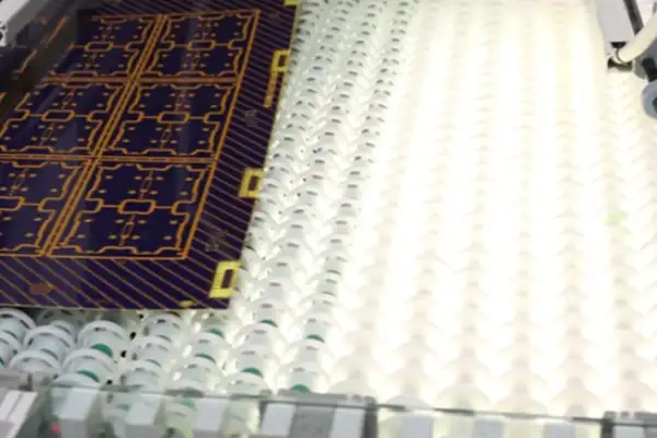
Battery Monitoring System PCB: Why the Hardware Foundation Determines Everything Else
BMS reliability isn’t decided by algorithms — it’s decided by the PCB
In PCB design discussions, some people treat vias as simple connection points, but this approach can cause problems in actual projects. I also learned this the hard way when I first started working with high-speed circuits—signal lines with neat routing would show obvious waveform distortion after passing through a few vias. Later, testing with a vector network analyzer revealed the problem lay in those inconspicuous metallized vias.
Many people think PCB vias are simply channels for signals on different layers. However, the situation is completely different when you raise the signal frequency to the GHz level. I remember once debugging a gigabit Ethernet interface and constantly experiencing packet loss. After two days of troubleshooting, I discovered that four series vias between the PHY chip and the transformer were causing impedance abrupt changes. Replacing two of them with blind vias immediately solved the problem.
Now, when designing layouts, I pay special attention to the parasitic parameters of vias. Each via introduces approximately 0.5pF of capacitance and 1nH of inductance. This may be negligible in low-frequency circuits, but it’s enough to cause reflections and ringing on high-speed signal paths, especially clock lines and differential pairs. I try to use as few vias as possible, and when they are necessary, I control the anti-pad size to optimize impedance continuity.
I recently helped a friend modify a communication board. His original design densely used 0.3mm micro-vias in the BGA area. However, power integrity testing showed the resonant frequency fell precisely within the chip’s operating frequency range. By adjusting the via layout of the DC blocking capacitors on the power layer, we moved the resonant frequency to a safer range. This case made me realize again that vias are not just connection tools, but also a key factor affecting electromagnetic compatibility.
Some engineers like to pursue the smallest via diameter, but this requires a trade-off. While small vias save space, they demand higher drilling precision and electroplating processes, easily leading to uneven copper plating. I generally leave a margin based on the PCB manufacturer’s capabilities; for example, for an 8-layer board, use at least 0.2mm via diameters rather than blindly pursuing 0.1mm.
Most easily overlooked is the impact of vias on heat dissipation. Insufficient vias on high-current paths can create thermal bottlenecks. Once, while working on a motor drive board, a miscalculation of the number of thermal vias below the power transistor caused a temperature rise 15 degrees Celsius higher than expected. Only after creating a thermal resistance model of the vias in simulation software was the balance point found.
Ultimately, PCB design is about resolving various contradictions. Via optimization is a prime example: ensuring reliable connections while controlling parasitic effects, saving space while considering manufacturability. Each PCB design is like walking a tightrope, requiring finding the perfect balance based on specific needs.
I’ve always felt many people misunderstand the small vias on PCBs. They seem to think that simply connecting the wires is enough. But when you start working with high-speed design, you realize that every via is a challenge.
I remember the first time I did DDR4 routing, I used a bunch of conventional vias, resulting in a completely blurred signal eye diagram. Later, I discovered that the reflections from those vias were the culprit. This made me realize that at GHz frequencies, current doesn’t travel in straight lines but rather along the conductor surface; those via stumps act like tiny antennas, constantly radiating energy outwards.
A common misconception is that making vias smaller solves the problem. In reality, a 0.3mm diameter micro-via can actually introduce larger parasitic capacitances in certain scenarios. The key is controlling its depth and location. I’ve seen people blindly stack vias under BGAs, resulting in impedance jumps that are more severe than the signal lines themselves.
What truly changed my perspective was during a debugging session on a 20-layer board. We experimented with different via anti-pad sizes and found that increasing the isolation ring by 15% significantly improved crosstalk. This was far more effective than simply increasing the number of vias. Sometimes, the most inconspicuous non-metallic areas are what determine signal quality.
Now I focus more on how current finds its way home, especially for vias that cross split regions. If the reference layer is incomplete, even the best simulation model can’t save you. I once saw a design that jumped back and forth between power planes, resulting in noise directly coupling into the clock line.
Actually, there’s no need to overcomplicate vias; they’re just necessary channels. But you need to know when to use ordinary vias and when to use back-drilling or even laser microvias. Once, I insisted on using vias filled with conductive adhesive in a 25G serial link. Although the cost was higher, it resulted in a more stable impedance profile.
Ultimately, good high-speed design isn’t about eliminating vias, but about making them behave properly—silent when they should be silent, and conducting when they should be reliable. I increasingly feel that PCB layout is a bit like playing Go; every move requires considering ten moves ahead, and vias are those seemingly insignificant but crucial intersections that determine victory or defeat.
Every time I see those densely packed PCB vias, I’m reminded of the pitfalls I encountered when I first started working with high-speed circuits. Back then, I always thought that just connecting the wires was enough, right? The result was terrible signal quality.
Many people easily overlook a crucial point: we always focus on the traces, forgetting that those inconspicuous vias are the real hidden killers. Especially in high-frequency environments, their impact is far greater than imagined.
The most typical problems I’ve encountered are reflections and crosstalk. In one project, despite neat routing, inexplicable interference kept appearing. Later, I discovered that the vias in several key locations were poorly designed. Those seemingly tiny parasitic capacitances accumulated and produced a significant delay effect.
Pad design is even more interesting. Some people like to make pads extremely large, thinking it’s more reliable, but actually, it increases parasitic effects. My current practice is to control the pad size as much as possible, just enough to meet process requirements. After all, every extra area adds unnecessary capacitive load.
I remember once debugging a board where the clock signal was constantly jittering. After a lot of troubleshooting, I finally discovered the problem was with the buried vias on the inner layers. The coupling between them and the power layer was much stronger than expected. This lesson taught me not to just look at the surface layout.
Now, when designing, I pay special attention to the placement of vias, trying to avoid sensitive areas. Sometimes, I’d rather have an extra loop to ensure a clean path for critical signals; this is much less troublesome than fixing things afterward.
What truly changed my mindset was redesigning an interface module. After optimizing all the via parameters, the eye diagram quality improved by a whole level—more noticeable than replacing the chip with a more expensive one.
So now, in every layout, I consider vias as active components rather than passive connection points. This shift in thinking has significantly stabilized the quality of my designs. You can try it too.
I always feel that many people overcomplicate PCB vias. Sometimes seeing those complex calculation formulas gives me a headache—not that they’re useless—but in actual design, there are often more intuitive ways to judge them.
I remember once encountering an interesting phenomenon while working on a high-frequency board: despite having theoretically calculated sufficient anti-pad gaps—the D2-D1 parameters—the measured capacitance was still significantly higher than expected. I later realized that excessively fragmented planar layers actually negatively impact overall performance—like suddenly adding too many tollbooths on a highway—while the delay at each individual tollbooth might be small, the overall traffic flow collapses. This is especially problematic when handling multi-GHz signals; the impedance discontinuities caused by planar fragmentation trigger noticeable signal reflections, much like turbulence created by water encountering boulders. Using a TDR instrument, I could clearly see multiple spikes in the impedance curve, a reality that theoretical calculations often fail to capture.
Speaking of the SLPCB model—I think its greatest value lies in reminding us to pay attention to the current return path—especially when handling differential signals—two vias placed too close together create additional coupling; two vias placed too far apart disrupt symmetry—finding this balance requires practical debugging experience. For example, in 10Gbps SerDes interface designs, we often use elliptical anti-pads to optimize isolation between differential pairs, while fine-tuning the coupling capacitors by adjusting the size of non-functional pads (NFPs). This fine-tuning often requires iterative iterations using electromagnetic field simulation tools; simply relying on geometric spacing formulas often yields limited results.
In a recent project, we tried a new method: placing the vias of the power bypass capacitors directly on the edge of the capacitor pads—instead of the traditional center position—although this deviates from textbook recommendations—but actual measurements showed a reduction in parasitic inductance of approximately 15%. Of course, this approach demands higher placement precision—requiring prior communication with the soldering plant regarding process capabilities. In fact, this edge-out via method shortens the current loop area, making it particularly suitable for powering BGA-packaged chips. We even experimented with symmetrical vias on both sides of the pads to form parallel paths, further reducing the equivalent inductance, but care must be taken to avoid excessive cutting of the pad copper, which could affect mechanical strength.
In fact, the most easily overlooked aspect of VIA design is material properties—the same geometric dimensions can exhibit significant differences on different substrates. For example, once when switching substrate suppliers, even with the same nominal dielectric constant, the resonant point shifted by 10%. It turned out to be due to different fiberglass cloth weaving methods. For instance, although 1080 and 2116 fiberglass cloths have similar nominal Dk values, differences in the local dielectric constant distribution at fiber bundle intersections can significantly affect phase consistency in the millimeter-wave band. This lesson has led me to now require suppliers to provide detailed material structure diagrams when doing high-frequency designs.
I increasingly feel that good VIA design is more like urban planning—ensuring the rationality of individual buildings while also considering the coherence of the overall traffic flow. Simply pursuing perfection in a single parameter can cause system-level problems. This is why I always advise novice engineers to focus on measured data rather than obsessing over theoretical calculations—after all, circuit boards are ultimately for powering up, not for solving math problems. For example, the layout of via arrays must consider thermal expansion coefficient matching; otherwise, CTE mismatch can easily lead to solder joint cracking during temperature cycling tests. Once, a heat dissipation via design we made failed to consider the thermal deformation difference between the aluminum substrate and FR4, resulting in microcracks in a low-temperature environment.
There’s a little trick to via layout for differential pairs: you can intentionally make a small bend in the inner layer routing—allowing the layer transition point to fall in a more spacious area—this provides enough space for the anti-pad—although it increases the trace length slightly—it greatly helps maintain impedance continuity. In practice, we use 3D electromagnetic simulation to check the field distribution in the layer transition area, and sometimes even use back-drilling technology to remove excess via stumps, like pruning branches to make the trunk clearer. Especially in high-speed links above 25G, this proactive optimization can effectively reduce resonance spikes on the insertion loss curve.
Sometimes I laugh out loud when I look back at boards I designed five years ago—back then, I always thought that the denser the vias, the better—now I actively leave breathing space for each via—this change in design philosophy is probably what growth is all about. Now I pay more attention to the transition structure between vias and transmission lines, such as using a gradually tapered transition section to smooth impedance changes, just like a highway ramp needs a reasonable buffer zone. I’ve recently been experimenting with adding grounding shielding via arrays around vias, which has proven highly effective in suppressing electromagnetic leakage in the 72GHz band.
I’ve always felt that many people misunderstand PCB design—they focus on routing rules while neglecting seemingly insignificant details. Take vias, for example; although small, their handling often determines the success or failure of the entire board.
I remember once debugging a high-frequency board where signal integrity consistently fell short of expectations. After two whole weeks of troubleshooting, we discovered the problem lay in a seemingly perfect via. The via’s pad design perfectly conformed to standard specifications, but those extra few millimeters of residual solder created a resonance effect at high frequencies. We then tried back-drilling to remove the excess copper layer on the via walls, and the problem was immediately solved. This experience made me realize that sometimes the most easily overlooked areas are precisely where meticulous attention to detail is needed.
The quality of vias largely depends on the electroplating process during manufacturing. I’ve seen many factories cut corners in the electroplating stage to save costs, resulting in severely insufficient current-carrying capacity in the vias and causing problems with the boards shortly afterward. Truly reliable vias require a uniform copper layer covering the entire via wall, especially for those with high aspect ratios. Uneven electroplating can easily lead to breakage or overheating later on.
Another point concerns via placement. Many people like to place vias close to component pads, thinking this shortens the path. However, blindly pursuing close proximity can cause problems. For example, solder can easily flow along the vias during soldering, leading to cold solder joints. I now prefer to maintain a proper distance between the vias and pads, allowing sufficient space for soldering, while ensuring electrical performance.
In fact, there’s no absolute standard for via design. It often requires flexible adjustments based on the specific application scenario. For example, for boards with high heat dissipation requirements, I might increase the number of vias and enlarge the via diameter. For high-density boards with limited space, I focus more on optimizing the via layout to avoid them consuming valuable routing resources. These experiences are accumulated gradually through trial and error; there’s no lofty theory, just practical experience.
When designing circuit boards, many people only focus on the rationality of component placement and the smoothness of routing, neglecting the impact of seemingly insignificant details. Take PCB vias, for example. Although they are just small holes connecting different layers, their presence becomes particularly noticeable in high-frequency environments.
I’ve seen many novice engineers arbitrarily add vias during routing, thinking that as long as they are connected, it’s fine. In reality, each via introduces parasitic capacitance and inductance. When signals pass through these tiny structures, additional delay and distortion occur.
Especially when dealing with high-speed digital signals or RF circuits, these subtle effects accumulate to form significant interference. For instance, in power distribution networks, multiple vias connected in series increase the equivalent inductance, degrading power quality.
The essence of inductance is its ability to impede changes in current, and this impediment is amplified in high-frequency circuits. Even if the inductance of a single via is small, the impedance it generates during rapid signal switching is enough to alter waveform quality. I once debugged a case where improper via placement on the ground plane caused ringing in the clock signal.
Parasitic parameters are not constant; they exhibit different characteristics as frequency increases. This means that designs that may be harmless at low frequencies will reveal problems at high frequencies. This frequency dependence renders simple rule-based judgments unreliable, necessitating verification through simulation.
What’s most troublesome is that these effects are often not independent; capacitors and inductors can couple to form more complex resonance phenomena. Sometimes, even when each component meets specifications, the overall performance may still fall short of expectations, which is very likely due to these parasitic effects.
Good design practice involves considering these potential problems early on, rather than trying to fix them later. Properly controlling the number of vias and optimizing their placement can significantly improve circuit stability, which is far more effective than adding compensation circuitry afterward.
BMS reliability isn’t decided by algorithms — it’s decided by the PCB
Beamforming performance depends on phase coherence across every antenna element — and
A relay control board that works perfectly in the lab can fail
- Experte für die Produktion kleiner bis mittlerer Chargen
- Hochpräzise PCB-Fertigung und automatisierte Montage
- Zuverlässiger Partner für OEM/ODM-Elektronikprojekte
Geschäftszeiten: (Mo-Sa) von 9:00 bis 18:30