
From Novice to Expert: Sharing My Experience in Pin Header PCB Selection
As an electronics enthusiast, I’ve come to understand firsthand the impact of
I have always found the PCB design for network switches to be a particularly fascinating field. Many people, right from the start, get hung up on which board material to use or how many layers are required to be considered “high-end.” In reality, however, it is often the fundamental aspects that are most easily overlooked.
I recall an instance while debugging a Gigabit switch board: despite utilizing high-quality materials, we were experiencing packet loss. We eventually discovered that the issue stemmed from improper handling of signal reference planes during routing, which resulted in severe crosstalk. That experience taught me a valuable lesson: even the finest materials cannot compensate for a poor layout.
Speaking of differential pair design, many engineers assume that simply routing two traces in parallel is sufficient; in reality, it is not that simple. The critical requirement is to maintain consistent spacing and a uniform electromagnetic environment for the pair throughout its entire path. If the spacing changes—for instance, when passing through vias or navigating corners—the characteristic impedance shifts, and signal quality suffers immediately.
I personally prefer to implement localized ground plane segmentation near critical high-speed interfaces to provide a clean return path for sensitive signals. This approach is far more practical than blindly increasing the total number of board layers.
Another point—one that is frequently underestimated—is the routing of clock signals. Some engineers treat them as ordinary low-speed signals, routing them haphazardly, only to find that the timing of the entire system falls into disarray. I have now made it a habit to treat clock traces as “priority-protected assets,” routing them well away from any areas that could potentially introduce interference.
Ultimately, PCB design is a balancing act involving a multitude of factors; there is no single “absolutely perfect” solution—only the choice that best fits the specific requirements at hand. Every time I lay out a new board, it presents a fresh challenge—and that is precisely why, to this day, I continue to find such joy in this work.
I have encountered far too many engineers who, when designing network switch boards, become overly fixated on theoretical parameters. While those complex formulas are certainly useful, in practice, you’ll often discover that the true drivers of performance are unexpected details. For instance, our team once spent two weeks optimizing impedance matching, only to eventually realize that power supply ripple was the actual culprit behind excessive signal jitter.
Speaking of impedance control, many people assume that simply routing traces according to calculated values is sufficient. However, batch-to-batch variations in PCB laminate materials alone can cause actual impedance to deviate by as much as 8%—not to mention the thickness variations that occur after the lamination process in multilayer boards. We subsequently adopted a standard practice: for every new batch of laminate material, we first fabricate and test a set of test coupons. The dielectric constant values measured in these real-world tests prove far more reliable than the parameters provided by the supplier.
Crosstalk is a particularly fascinating issue. I recall a time while debugging a 25G port: even though the trace spacing strictly adhered to the “3W rule,” the eye diagram consistently displayed glitches. A subsequent TDR measurement revealed that the problem stemmed from coupling between vias on adjacent signal layers—demonstrating that the 2D design rules found in textbooks are simply inadequate for real-world 3D layouts. We now make a point of staggering the vias for high-speed signals by at least half a millimeter; while this consumes slightly more board real estate, the resulting improvement in signal stability is dramatic.
Ironically, power distribution is often the most overlooked aspect of the design process. I remember a project where, in the early stages, we opted for standard decoupling capacitors to save costs; consequently, the 10GbE ports experienced bit errors whenever they were running under full load. Switching to low-ESR capacitors resolved the issue immediately—and the total cost increase for the entire board amounted to mere dollars. This experience taught me a valuable lesson: sometimes, the most expensive solution actually turns out to be the most cost-effective one—after all, no one wants to face product recalls or costly rework after a product has already hit the market.
The 400G network switches I’ve been working on recently present an even greater challenge. As signal speeds climb to 56Gbps, even subtle factors—such as the weave pattern of the fiberglass fabric within the PCB laminate—can significantly impact signal loss. We experimented with base materials from various manufacturers and discovered that while certain laminates specifically designed for high-frequency applications cost 30% more upfront, they ultimately eliminate the need for costly *redrivers* later in the design cycle. These types of trade-offs are inherent to every project; the key to success lies in conducting thorough validation testing early in the process.
Ultimately, PCB design is much like cooking: simply having the recipe isn’t enough; you need to get your hands dirty and learn through trial and error. Standard specifications serve merely as a baseline—a passing grade, at best. To truly create a masterpiece, you must rely on the accumulated wisdom of practical experience.
I’ve always found the world of network switch boards and cards to be a truly fascinating field. I remember one time I was helping a friend troubleshoot some equipment; when I opened up the casing and saw the dense, intricate network of circuitry inside, I realized that this stuff was far more complex than I had ever imagined.
Those tiny holes on the circuit board are actually critically important. I used to think that drilling holes was just a mechanical chore—how hard could it be? But after witnessing the manufacturing process firsthand, I discovered that the position and depth of every single hole must be precise down to the micron level. Even a slight deviation can compromise the entire signal transmission.
The most extreme example I’ve ever seen was a board featuring over twenty layers of circuitry stacked on top of one another. During the lamination process, these multi-layer structures are highly susceptible to expansion and deformation issues. If not controlled meticulously, the final drilling stage might result in holes that completely miss their intended target positions.
The testing phase is often the most easily overlooked part of the process. Many people assume that as long as the board powers up, it’s good to go; in reality, it involves much more than that. You have to ensure that every single trace transmits signals stably and that the board can withstand the rigors of prolonged, high-load operation.
With the rapid advancement of high-speed networking today, the demands placed on circuit board materials are becoming increasingly stringent. Traditional substrate materials are starting to fall behind the times, necessitating the search for new dielectric materials to minimize signal loss.
Sometimes, as I gaze at these precision-engineered circuit boards, I reflect on the fact that they represent the culmination of an entire manufacturing ecosystem. From the initial design concept to the final round of testing, every single stage must be executed to perfection to guarantee the stable operation of network equipment.
Several projects I’ve recently been involved with have focused on leveraging more advanced manufacturing techniques to boost circuit board performance. While I can’t go into specific details, I can certainly sense that this field is currently undergoing a rapid cycle of technological iteration.
Ultimately, a high-quality circuit board serves as the very skeleton of a network; it doesn’t process data directly, yet it dictates how fast and how stably the entire system can run. The next time you use a piece of network equipment, take a moment to consider the sheer amount of precision engineering and accumulated technical expertise hidden within it.
I’ve long felt that many people’s understanding of network switches remains purely superficial. Whenever I see people discussing equipment performance while focusing solely on chip specifications, I feel compelled to remind them not to overlook the foundational element: the PCB. This is especially critical in scenarios involving massive data throughput, where a standard, run-of-the-mill circuit board simply wouldn’t be able to handle the heavy operational load.
I recall an instance last year when I was helping a friend’s company upgrade their network infrastructure. The switches they had purchased performed adequately during initial testing; however, the moment dozens of devices were connected simultaneously, they began experiencing frequent packet loss. Upon opening the units, we discovered they were built using generic PCB materials, resulting in severe signal attenuation. The issue was ultimately resolved only after switching to specialized high-frequency, high-speed PCB materials.
In reality, as the number of ports increases and transmission speeds rise, the demands placed on the PCB become increasingly stringent. I have seen instances where manufacturers, in an effort to cut costs, compromised on the quality of their PCB materials—a decision that ultimately resulted in entire batches of equipment requiring rework. This is particularly critical in server room environments that demand 24/7 uninterrupted operation; standard circuit boards simply cannot withstand such prolonged, high-load conditions.
Many enterprises are now beginning to deploy 10-Gigabit networks, which places even higher demands on the circuit boards within their network switches. High-frequency signals are particularly susceptible to interference during transmission; if the quality of the PCB material is substandard, even the most advanced chipset will be unable to deliver its full performance potential.
An interesting phenomenon I’ve observed is that switches with identical specifications can exhibit a performance gap of over 30% in real-world usage, simply because they utilize different grades of PCBs. This reminds me of a project I worked on previously, where I tested two 48-port switches. Although they shared the exact same chipset, significant differences in their circuit board designs meant that one could maintain latency within the microsecond range even under full load, while the other frequently suffered from latency spikes reaching the millisecond range.
I believe that when selecting a network switch, one should not focus solely on surface-level specifications, but must pay even closer attention to the quality of the internal components. After all, the PCB serves as the device’s skeletal structure; even the most powerful chipset requires a reliable physical foundation to truly unleash its full capabilities.
While recently analyzing the design of network equipment, I stumbled upon an intriguing observation: many manufacturers today boast extensively about the sophisticated HDI (High-Density Interconnect) processes they employ to fabricate their switch motherboards. Yet, to be honest, this marketing rhetoric often overlooks the most fundamental issue: true performance enhancement stems not from merely stacking layers upon layers of blind and buried vias, but rather from the inherent soundness and logic of the overall architectural design.
I recall disassembling an enterprise-grade switch last year; its PCB was densely populated with micro-via designs. While it certainly looked aesthetically impressive, I noticed that the signal transmission paths had been rendered excessively complex—a design choice that, ironically, increased the risk of signal integrity issues. Sometimes, the simplest direct-connection approach proves far more reliable than a flashy, overly intricate HDI structure.
Speaking of interconnect design, I’ve noticed that many engineers become so fixated on achieving maximum routing density that they inadvertently neglect fundamental elements such as thermal management and electromagnetic compatibility (EMC). During one particular test, a standard 8-layer PCB—when paired with a sensible layout—actually demonstrated greater stability than certain solutions that boasted the use of “any-layer interconnect” technology. This experience reinforced my realization that technical selection should not be driven solely by specifications on paper, but must also take into account the specific context and requirements of the actual application scenario.
There is currently a common misconception within the industry—a prevailing belief that simply adopting high-end HDI technology will automatically resolve every technical challenge. However, what truly impacts network switch performance are often those seemingly ordinary details—such as the optimization of the power distribution network and measures for isolating clock signals. If these foundational tasks are not executed properly, even the most advanced manufacturing processes will be entirely in vain.
The most egregious design I have ever encountered involved cramming over twenty layers of blind and buried vias onto a single board; consequently, poor thermal management caused the chips to frequently throttle down their clock speeds. In contrast, some boards utilizing traditional manufacturing processes—yet featuring a well-conceived layout—have proven capable of operating stably over the long term. This experience has further solidified my conviction that, when designing network equipment, one must not blindly chase after technical specifications but rather prioritize overall balance.
In fact, from an engineering perspective, a robust interconnect design should resemble building with blocks: each module should maintain clear interface relationships with the others, rather than having every function crammed onto a single board. A modular approach is often far more practical and flexible than the ceaseless pursuit of ever-higher routing densities.
Ultimately, the choice of PCB-Herstellung technology depends entirely on specific requirements. For most enterprise environments, overly complex HDI (High-Density Interconnect) designs may actually constitute a wasteful extravagance; doing the foundational work right—making it solid and robust—remains the golden rule.
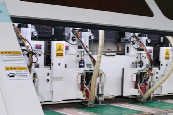
I have recently been delving into the various circuit board design challenges inherent in network equipment. You might assume that a PCB is merely a matter of connecting a few wires; however, once you actually undertake the task, you quickly realize it is far from that simple—particularly when dealing with the multi-layer boards utilized in network switches.
I recall an instance where our team encountered a rather instructive situation while designing a board for an enterprise-grade switch. In an effort to accelerate our schedule, we decided to simply reuse a previous layout scheme—a decision that ultimately caused us to stumble. The signal transmission in the new design proved consistently unstable; we later discovered that the issue stemmed from a poorly planned distribution of the power and ground planes, which compromised signal integrity.
In reality, the greatest pitfall when designing such high-density boards is making assumptions. You might assume that simply establishing electrical connectivity between points is sufficient; however, high-frequency signals do not behave that way. They tend to interfere with one another in places where they shouldn’t—much like being in a room where a dozen people are all shouting at once, making it impossible to clearly discern what anyone is saying.
Consequently, I now place a tremendous emphasis on integrity checks during the design phase. This entails more than merely running automated verification tools; it requires thinking from the perspective of the entire system. For instance, could the power distribution network adversely affect signal quality? Could the thermal management design lead to changes in material properties? These seemingly unrelated factors often ultimately manifest as issues with signal integrity.
There is one piece of wisdom I consider particularly valuable: do not rely too heavily on automated routing software. While many of today’s tools are highly intelligent, they ultimately lack an understanding of your specific application context and operational environment. I typically begin by manually planning the routing for critical signals—prioritizing the most sensitive sections first—before handing the remainder over to automated tools for processing.
Material selection is another aspect that is easily overlooked. Substrates made of different materials exhibit vastly different performance characteristics at high frequencies; sometimes, in an effort to save a little on costs by choosing cheaper materials, one ends up spending even more time on debugging later down the line.
The manufacturing phase, in particular, can be a real headache. No matter how excellent a design is, it is all for naught if the factory’s manufacturing processes fail to keep pace. I once encountered a situation where impedance control failed due to uneven copper plating thickness, ultimately forcing us to resubmit the boards for fabrication.
As I continue working on PCBs for network switches, I increasingly view the process as a comprehensive systems engineering endeavor. From the initial conceptualization of the design to the final finished product, every single stage demands meticulous attention. Sometimes, a single minor oversight can result in the entire project being delayed by several weeks.
Nevertheless, these challenges are quite engaging; I learn something new every time I solve a novel problem. The sense of accomplishment—especially when I see a board I designed operating stably in a real-world environment—is truly gratifying.
While recently researching network equipment, I observed an interesting phenomenon: many people tend to focus their attention on the flashy, high-level specifications while overlooking the fundamental basics. For instance, when discussing network switches, we often fixate on the specifications of the switching chips; yet, what truly determines the device’s stability is often that seemingly unremarkable PCB.
I recall an incident last year where I helped a friend debug a switch that was constantly dropping packets. Upon opening the unit, we discovered the problem lay in the routing near the power supply module, which had been placed too close to the high-frequency signal zones. Such minute details are completely invisible in a datasheet, yet they can cause endless headaches during actual operation.
Today’s high-speed networking environments impose increasingly stringent requirements on PCB design—particularly regarding the routing of differential pairs for high-speed signals. I have seen designs where, in an attempt to cut costs, engineers opted for standard FR4 materials; consequently, the 56Gbps signals failed to transmit stably. It is akin to attempting to race a Formula 1 car on a standard public road: the problem lies not with the vehicle itself, but with the road’s inability to handle the demands placed upon it.
While the switching chips are undoubtedly crucial, even the most advanced chips require a reliable physical platform to function effectively. The task of routing out those densely packed pins—while simultaneously ensuring signal integrity—truly serves as a rigorous test of one’s design prowess. It is often quite amusing to observe certain manufacturers who proudly tout the use of cutting-edge switching chips in their marketing materials, yet conveniently sidestep any mention of the actual PCB design—a rather telling example of selective presentation.
Indeed, after working in hardware design for a significant period, one eventually realizes that every single stage of the process is inextricably interconnected. For instance, while the design of a clock circuit may appear simple, providing a stable timing reference for an entire system is no easy feat. I have encountered cases where interference with the clock signal caused the performance of an entire network switch to drop by half.
Thermal management is another critical factor. High-performance chips consume significant power; if the thermal design of the PCB is inadequate—no matter how powerful the chip itself may be—it will inevitably throttle its clock speed due to overheating. This is akin to asking an athlete to run while wearing a padded winter coat; even with the finest physical conditioning, they would be unable to perform at their full potential.
Ultimately, hardware design is a systems engineering discipline; one cannot simply fixate on a single standout feature in isolation. Much like building a custom PC—where simply having a top-tier CPU is insufficient, as the RAM, motherboard, and power supply must all be properly matched—the same principle applies to network equipment. While the chips are undoubtedly crucial, the PCB serves as the device’s skeletal structure, supporting and enabling all components to work together in harmony.
At times, I find myself wondering if the industry places too much emphasis on the performance of individual components while neglecting overall system synergy. After all, what users truly seek is a stable and reliable network experience—not merely a collection of flashy technical specifications. No matter how impressive the numbers look on paper, they are rendered meaningless if the device suffers from actual packet loss.
This may well explain why certain older device models—despite possessing less dazzling specifications—often prove to be more durable than their newer counterparts. They have undergone more extensive real-world validation, and every aspect of their design has been more thoroughly refined and harmonized.
Therefore, the next time you see a manufacturer heavily promoting a specific chip, consider asking this follow-up question: “But is the design of the underlying platform—the ‘vehicle’ for that chip—truly up to the task?”
While recently researching network switch PCB designs, I observed an intriguing phenomenon: many people tend to focus excessively on high-level, sophisticated technical parameters, while overlooking the most fundamental principles of design logic. Take a network switch PCB, for instance: what truly determines success or failure is often not the inherent sophistication of the chips themselves, but rather how effectively those various components are orchestrated to coexist harmoniously within a confined physical space.
I recall once disassembling a network switch from a well-established manufacturer; upon opening the casing, I was absolutely blown away by the layout of the PCB inside. Although it utilized a standard eight-layer board design, the interplay between the power partitioning and signal routing was nothing short of a work of art. This was particularly evident in the area surrounding the switching chip, where the clock synchronization challenge was ingeniously resolved using nothing more than simple serpentine routing—a far more clever approach than merely piling on expensive materials.
Many engineers today tend to fall into a common trap: the belief that only top-tier substrate materials can ensure effective high-speed signal transmission. In reality, with proper design, standard FR-4 material is perfectly capable of meeting the requirements of most commercial network switches. The key lies in truly grasping the essence of signal integrity; rather than obsessing over a board material’s dielectric constant, one is better off focusing on optimizing routing spacing.
One particular test left a lasting impression on me. Using the exact same switch chip, two PCBs designed with different philosophies exhibited a performance disparity of up to 30%. Where did the problem lie? Surprisingly, it was traced back to the improper placement of thermal vias, which resulted in localized “hot spots.”
This case study made me realize that designing a network switch is truly a holistic systems engineering endeavor—one where a change in any single element can ripple through and affect the entire system.
Speaking of thermal management, I’ve noticed that many teams expend excessive energy calculating heatsink dimensions while overlooking the far more critical task of planning thermal conduction paths. For instance, strategically arranging arrays of thermal vias to channel heat toward the metal enclosure often yields more immediate and effective results than simply increasing the size of the heatsink.
Recently, while helping a friend refurbish an older network switch, I experimented with a novel approach: I reconfigured the layout of the traditional fiber-optic module interfaces to prioritize routing the high-speed signal traces through the inner layers of the PCB. Although this increased the total number of vias required, the results of the electromagnetic compatibility (EMC) testing actually improved by two performance grades.
This willingness to break with convention has further reinforced my conviction that excellent PCB design is never merely a matter of rigidly following a prescribed formula. Sometimes, looking at the older switches running in our lab—some of which have been in continuous operation for five or six years—I find that they are actually more stable than our brand-new equipment.
While the components used in those older units may appear obsolete by today’s standards, the rigorous design philosophy behind their layout remains profoundly worthy of study. Modern design trends often prioritize the extreme optimization of technical parameters, yet in doing so, they risk forgetting that an electronic device is, at its core, a work of art that demands a delicate balance.
I’ve always found the design of network equipment to be a particularly fascinating field. Many people tend to focus on the tangible, visible aspects—such as chip performance or software functionality—but I am far more intrigued by how the subtle, often-overlooked physical details influence the overall performance of the entire system.
Take the PCB inside a network switch, for instance. The layout of this board is, in reality, a tapestry woven from countless design trade-offs. Consider, for instance, those densely populated regions filled with connectors; whenever I watch engineers repeatedly tweaking impedance models just to determine the optimal placement for a handful of vias, it strikes me as a truly authentic glimpse into the realities of the engineering craft. It is not simply a matter of establishing a connection and calling it a day.
I have seen instances where aspects of a project that were overlooked during the initial stages later evolved into major headaches. One example stands out clearly in my memory: during testing, the port section of a rack-mounted network switch consistently exhibited excessive electromagnetic radiation leakage. After extensive troubleshooting, the root cause was traced back to the specific PCB traces running between the network transformer and the RJ45 connector.
Although this particular trace segment appears quite short, if not handled correctly, it can act as a highly effective antenna, leading to pronounced electromagnetic radiation effects.
In reality, the issue of electromagnetic compatibility (EMC) is far more complex than one might imagine. There are times when you have followed standard best practices—implementing a complete ground plane and adding ample decoupling capacitors—yet actual testing still reveals inexplicable interference.
At such junctures, it becomes necessary to step back and re-evaluate the fundamental component layout to ensure its logical soundness. The placement of the transformer, in particular, is absolutely critical.
Its very purpose is to provide electrical isolation; however, if the underlying reference plane is poorly managed, or if its physical integration with the connector is not sufficiently tight, it can inadvertently introduce a whole new set of problems.
I tend to favor an approach where these interface components are treated as a cohesive system right from the initial design phase, rather than handling each part in isolation.
Some of the newer designs I have encountered recently have begun adopting highly integrated solutions, creating a much more compact and tightly coupled assembly of the transformer and connector. This approach indeed proves effective in mitigating many potential radiation risks.
However, this also introduces new challenges—for instance, it can complicate thermal management and increase the difficulty of maintenance and repair.
Such is the nature of hardware design: one must constantly strike a balance between competing requirements. There is no single “set it and forget it” solution; every project presents its own unique circumstances that demand specific, case-by-case analysis.
What I find most fascinating is that these seemingly mundane engineering details often serve as the ultimate determinants of a product’s final quality. These are insights you won’t find in a standard datasheet; they can only be acquired through the accumulation of practical, hands-on experience.
The process of relentless debugging—working tirelessly until a device finally passes rigorous testing—can be grueling. Yet, it is precisely through this ordeal that one gains a wealth of knowledge. Perhaps that is the true allure of hardware design: every time you solve a problem, you walk away with a new lesson learned.
As an electronics enthusiast, I’ve come to understand firsthand the impact of
Why is green the universal choice for circuit boards? Behind this seemingly
As a hardware entrepreneur, I often see teams fall into a trap
- Experte für die Produktion kleiner bis mittlerer Chargen
- Hochpräzise PCB-Fertigung und automatisierte Montage
- Zuverlässiger Partner für OEM/ODM-Elektronikprojekte
Geschäftszeiten: (Mo-Sa) von 9:00 bis 18:30