
Heat Dissipation Challenges and Solutions in PCB Circuit Board Design
Circuit boards are more than just that green board in a phone
I’ve always found the development trajectory of the microelectronics industry particularly interesting, especially those manufacturers focused on PCB manufacturing. They aren’t passively waiting for orders as we might imagine, but actively seeking their place in technological iterations. In recent years, the AI boom has indeed brought new variables to this industry. For example, many manufacturers that traditionally produce rigid boards are now also starting to explore the production of high-density interconnect substrates, because AI chips have much more stringent requirements for circuit boards than ordinary consumer electronics.
I know a small-to-medium-sized manufacturer that started transitioning to producing small-batch AI server substrates last year. They told me the biggest challenge wasn’t equipment investment, but rather controlling costs while ensuring signal integrity. After all, AI chips consume a lot of power and generate a lot of heat. The choice of substrate materials and lamination processes become particularly critical.
Globally, manufacturers in different regions are responding in completely different ways. European and American companies tend to focus on the high-end customized market, such as the specialized PCB needs in the aerospace industry. They don’t pursue economies of scale as much. Japanese and Korean manufacturers, on the other hand, emphasize synergy within the semiconductor supply chain, especially in substrate and packaging/testing capabilities. This difference reflects the characteristics of their respective industrial systems.
Interestingly, many emerging microelectronics PCB manufacturers are now adopting a modular approach. They combine standardized PCB modules with customized substrates, which allows them to meet customers’ rapid iteration needs while maintaining a certain profit margin.
I think this industry will become increasingly differentiated in the future. On one side are substrate experts pursuing ultimate process technology; on the other are solution providers who can flexibly integrate resources. The space for simply manufacturing circuit boards will definitely shrink.
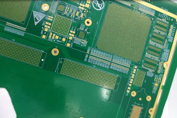
I’ve always felt that the most fascinating aspect of microelectronics lies in its unseen details. Take PCBs, for example. Many people might think of a circuit board as just a green board with a few lines. But what truly determines a product’s lifespan is often what’s hidden beneath the surface. I remember visiting a microelectronics PCB manufacturer’s production line once and discovering that their quality control was far more complex than I’d imagined. For instance, they use X-ray fluorescence analyzers to check the dielectric constant uniformity of the substrate when raw materials arrive at the warehouse. This control over material consistency directly impacts the signal integrity of high-frequency circuits.
Electrical performance testing is particularly interesting. Some manufacturers spend a lot of time on final inspections. But the truly professional approach is to integrate testing into every stage of production. For example, performing a basic continuity check immediately after etching, rather than waiting until all components are soldered to discover problems. After drilling, they also use an automated optical inspection system to compare the hole position accuracy with the deviations in the design documents, ensuring that the alignment error of multilayer boards does not exceed 25 micrometers.
I’ve seen many engineers rely too heavily on the data output of automated equipment. In reality, human experience remains irreplaceable in identifying certain hidden defects. Especially when PCBs need to withstand extreme temperature changes, simply looking at the numbers in the test report may not reflect the potential risks in real-world usage scenarios. Experienced technicians can use a microscope to detect minute cracks at the junction of copper foil and the substrate. These defects, which only gradually appear during thermal cycling tests, often cannot escape standard testing procedures.
Many manufacturers are now pursuing more precise circuit designs. However, excessively compressing space can introduce new problems, such as interference during high-frequency signal transmission. These details often require a combination of testing methods to detect. Relying solely on one testing method can easily leave blind spots. For example, a time-domain reflectometer can locate impedance discontinuities, while a vector network analyzer can fully characterize S-parameters; combining both is necessary for a comprehensive assessment of signal integrity.
Regarding environmental adaptability, I think the most easily overlooked aspect is the slow aging process during daily use. Accelerated aging tests in the laboratory can indeed detect problems. However, actual user habits vary greatly. For example, connectors that are frequently plugged and unplugged require special attention to their long-term stability. Some manufacturers use contact points with gold plating thicknesses exceeding 1.27 micrometers and verify durability through mechanical life tests of over 5000 insertion/removal cycles.
A European manufacturer’s approach greatly inspired me. They simulate various extreme usage scenarios during the sample stage, including accidental drops and liquid spills. This forward-thinking testing approach effectively improves product durability. They specifically designed multi-axis vibration tables to simulate transportation bumps and used salt spray chambers to test corrosion resistance. These unconventional tests often uncover unexpected weaknesses.
Ultimately, a good PCB not only needs to pass standard tests but also withstand the test of real-world use. This requires manufacturers to have a deep understanding of end-use scenarios, rather than simply copying industry standards. For example, automotive electronics need to focus on wide temperature range stability from -40℃ to 125℃, while medical devices prioritize insulation reliability under long-term power-on conditions.
Recently, I’ve noticed an increasing demand for customized testing, especially when PCBs are used in special environments. General-purpose testing solutions are often insufficient. This necessitates manufacturers’ ability to flexibly adjust testing processes. For example, the aerospace industry requires arc testing in a vacuum environment, while deep-sea equipment needs to verify its sealing performance under simulated high-pressure conditions.
From the user’s perspective, the most direct experience is whether the product is stable and reliable. All of this is built upon a rigorous manufacturing and testing system. For instance, using thermal imaging to detect current distribution uniformity and scanning electron microscopy to analyze weld interface quality—these sophisticated testing methods collectively construct a quality defense line.
Sometimes, seemingly simple circuit boards contain a wealth of accumulated technology. From materials science to signal processing, from mechanical engineering to chemical processes, each link requires a deep integration of professional knowledge. Impedance control, for example, requires simultaneously considering the interaction of multiple variables such as dielectric thickness, copper foil roughness, and even the dielectric constant of the solder mask.
The most fascinating aspect of this industry is that there are always new challenges to address. With the widespread application of 5G millimeter-wave technology, phase consistency testing of RF circuits has become a new challenge; and dynamic bending testing methods for flexible circuit boards are constantly evolving. This rapid pace of technological iteration is both stressful and exhilarating.
I’ve recently noticed an interesting phenomenon: microelectronics manufacturers specializing in high-end PCBs seem to be quietly shifting their focus. Previously, people might have paid more attention to changes in demand within the traditional consumer electronics sector; now, however, the wind has clearly shifted—especially as AI begins to see real-world applications.
A friend who designs circuit boards told me about their recent projects; they suddenly realized that over half were related to AI servers or high-performance computing devices. This reminded me of a factory I visited last year; they originally mainly produced standard multilayer boards, but now they’ve shifted most of their production capacity to HDI boards. The newly added laser drilling equipment in the workshop is running almost 24/7; workers are working three shifts and still can’t meet the orders.
This shift reflects a deeper issue: traditional PCB manufacturing processes can no longer keep up with the pace of AI hardware development. Look at the servers training large models now; the internal circuit board wiring density is frighteningly high; ordinary processes simply cannot meet the requirements. This forces manufacturers to move towards higher-end technologies, even if it significantly increases costs.
An engineer I know used a vivid analogy: it’s like suddenly switching from a regular highway to a multi-level transportation network. The microvia interconnect capability provided by HDI technology has become a crucial foundation for the explosive growth of AI computing power. Without these high-density interconnect boards, even the most advanced chips would be stuck in a rut.
Interestingly, this technological upgrade has brought new vitality to the industry. Previously, PCB manufacturing was considered a relatively mature field with limited room for innovation. Now, even small and medium-sized manufacturers are actively introducing new processes and developing product lines more suitable for the AI era. Although there may be short-term cost pressures, in the long run, it has indeed opened up new growth opportunities.
Of course, the challenges are not insignificant. Controlling the yield rate of high-end HDI boards is a major headache, not to mention dealing with increasingly stringent delivery cycles from customers. However, from another perspective, these pressures have actually accelerated the technological iteration of the entire industry. Sometimes breakthroughs happen when pushed to the limit.
Looking at the new testing equipment on the production line, I suddenly realized that this is no longer simply an upgrade in the manufacturing process. From material selection to process flow, every detail is redefining what constitutes a circuit board that meets the requirements of the AI era. This change may not be immediately noticeable, but its accumulated impact could be beyond imagination.
I’ve always found working in microelectronics quite interesting. People used to think of PCBs as just a few green boards—but things are different now. Especially the microelectronics PCB manufacturers that supply AI devices are getting creative.
The other day I saw a photo a friend posted: their newly designed board is so thin it’s translucent. This reminded me of the bulky circuit boards I saw when I first entered this industry ten years ago—who would have imagined that packaging technology would be so intertwined with PCB design back then? Many manufacturers are now trying to embed chips directly into the board—this method definitely saves space.
The most extreme example I’ve seen is a company that makes autonomous driving sensors—they’ve packed the entire processing unit into an area smaller than a fingernail—something unthinkable five years ago.
In fact, many innovations are hidden in the details—such as the way the circuits are arranged or the choice of materials—these seemingly insignificant changes often bring unexpected results.
There’s an interesting phenomenon: Previously, everyone liked to make things as big as possible—now, the pursuit is for extreme compactness—this reflects a redefinition of efficiency across the entire industry.
I’ve been pondering something lately: why are more and more designs breaking traditional boundaries? It’s probably because the data processing demands brought by AI are so unique—traditional approaches simply can’t handle them.
Sometimes, watching these new technologies makes me realize that the industry is truly changing—and changing much faster than we imagined.
I recently chatted with a friend who does hardware design and discovered an interesting phenomenon: many people believe that as long as the chip is powerful enough, electronic products are stable. In reality, the microelectronics manufacturers behind the circuit boards are the hidden giants who truly determine the lifespan of equipment. Think about it—consisting of high-frequency modules processing 5G signals: some start to experience signal attenuation after three months; others remain stable even under extreme temperature differences. This difference often stems from the control of material expansion coefficients during PCB manufacturing.
I remember last year our team tested a batch of microelectronic circuit boards used in industrial sensors. One manufacturer’s sample performed perfectly in the lab environment; however, after two weeks of continuous operation in the field, the impedance value became unstable. It was later discovered that the problem lay in the glass transition temperature of the substrate—the ordinary FR4 material they were using simply couldn’t withstand prolonged high-temperature environments. This incident made me realize the importance of choosing a professional microelectronics PCB manufacturer: they need to understand materials science, thermodynamics, and even signal integrity theory.
Many consumer electronics products now pursue thinner and lighter designs, which actually presents greater challenges to circuit boards. For example, the line width on mobile phone motherboards has reached below 20 micrometers, requiring manufacturers to have laser drilling capabilities and even master semi-additive processes. I’ve seen some traditional PCB manufacturers transitioning to microelectronics still using chemical etching processes, resulting in line edge roughness directly affecting the quality of high-frequency signal transmission.
Interestingly, excellent manufacturers often extend quality control to the very upstream of the supply chain. Once, during a visit to a Japanese manufacturer’s factory, I discovered that they even assessed the uniformity of crystal orientation of their copper foil suppliers—such attention to detail is truly admirable. After all, when the line spacing shrinks to one-tenth the diameter of a human hair, any fluctuation in raw material quality can cause a collapse in yield.
Recently, the field of autonomous driving has placed even more stringent requirements on microelectronics circuit boards. The PCBs for automotive radar modules must withstand the high temperatures and vibrations of the engine compartment and maintain stability in humid, salt-spray environments. This has prompted many manufacturers to research ceramic-filled substrates or use modified polyimide materials—innovations that are redefining the standards of reliability.
Having observed this industry for over a decade, I’ve found that the real technological divide isn’t in equipment specifications, but in the depth of a manufacturer’s understanding of the application scenario. Just as circuit boards for medical implants must consider biocompatibility, those for aerospace applications require radiation resistance—there are no one-size-fits-all solutions; each niche requires customized technological accumulation.
Sometimes, I feel that microelectronics manufacturing is akin to performing surgery: it requires both macro-level systems thinking and micro-level precision. When you see those gold wires thinner than spider silk under a microscope, you understand why this industry is considered the last line of defense for the reliability of technological products.
Having worked in microelectronics for a long time, you’ll find that the real arena for competition among top microelectronics PCB manufacturers is in the details. I’m not talking about fancy technical terms or the highest specifications in brochures. The real test of skill often lies in the fundamentals—such as the ability to control linewidth.
You might think that making a line width of tens of micrometers sounds impressive. But in actual production, it’s not that simple. I’ve seen many manufacturers produce very fine line samples to showcase their capabilities. But problems arise during mass production—the linewidth of one batch might be 20 micrometers, while the next batch might be 30 or even 40 micrometers.
This fluctuation can cause significant problems in practical applications.
I remember once testing samples from different manufacturers and discovering an interesting phenomenon. Two suppliers claimed to be able to achieve a linewidth of 25 micrometers, but under a high-powered microscope, the difference was obvious. One supplier’s lines had clear, straight edges, while the other’s edges were rough and looked like poorly drawn pencil lines.
This difference might be insignificant on ordinary circuit boards, but it becomes fatal in high-frequency signal transmission.
Truly excellent manufacturers don’t just focus on producing the finest threads; they are more concerned with ensuring that every thread maintains the same precision and quality. This requires a high degree of coordination throughout the entire production process, from material selection to process control—every step must be meticulous.
Sometimes, we focus too much on the most cutting-edge technical parameters and overlook these fundamental but crucial details.
In fact, many applications today don’t require pursuing the ultimate linewidth; stability and consistency are more important. A manufacturer that can consistently produce 30-micron lines is more valuable than one that can barely manage 15 microns with a low yield.
After working in this industry for a while, you’ll understand that true technical strength isn’t reflected in extreme data from the lab, but in the consistently high-quality products output daily on the production line.
The greatest strength of microelectronics PCB manufacturers that have earned long-term customer trust is often not how fine they can produce, but their ability to perfect every detail consistently.
This is probably the charm of manufacturing—true technical depth lies within seemingly tedious repetition.
I’ve always felt that modern electronic products are increasingly reliant on those small components hidden inside. Recently, chatting with some friends who work in hardware, I discovered that there’s so much intricacies behind these seemingly ordinary circuit boards. Especially for manufacturers specializing in microelectronic PCBs, the problems they face are far more complex than we imagine.
I remember last year, a project required finding a suitable manufacturer, only to discover that there weren’t many domestic companies capable of producing high-end microelectronic PCBs. It wasn’t that the technology was lacking, but rather that many manufacturers were busy transforming their business models. Profit margins for ordinary circuit boards are increasingly thin, and everyone is moving towards higher precision and reliability. This reminded me of a factory I visited before; they adjusted their entire production line for a tiny difference in trace width—an investment that most companies can’t afford.
Many people prioritize price when choosing a manufacturer, but I’ve found that what’s truly important is whether they can keep up with your pace. Some manufacturers offer low prices, but their lead times are incredibly long, ultimately causing delays. Especially for innovative products, if the manufacturer doesn’t understand your needs, even the best design is useless.
I’ve met some small overseas PCB manufacturers. They’re not large, but they excel at customized products. Sometimes they’re even more flexible than large manufacturers, depending on the specific requirements. It’s not that large manufacturers are bad, but the current market demands more diverse options.
Many innovations in the microelectronics field now lie in materials. For example, some new substrate materials allow for thinner and more heat-resistant circuit boards, but mass production of these new technologies requires manufacturers willing to collaborate and experiment. Finding a partner willing to learn from mistakes is truly difficult.
Ultimately, choosing a manufacturer isn’t simply about comparing prices and specifications; it’s more about finding a partner with whom you can grow. After all, nobody wants their product to fail because of a single circuit board, right?
Recently, I chatted with some friends in the hardware industry and discovered an interesting phenomenon: many people focus solely on equipment parameters when choosing a microelectronics PCB manufacturer. However, the true determinant of final product quality often lies in the unseen details and the ability to handle them effectively. For instance, one team working on a smart home project used an MCU chip from a major manufacturer but chose the lowest-priced PCB manufacturer. The resulting samples showed severe signal interference, which was later discovered to be due to excessive fluctuations in the dielectric constant of the substrate.
Truly reliable manufacturers will proactively discuss application scenarios with you, rather than simply asking how many layers of board you need. We encountered an interesting example while working on an industrial controller: using a 32-bit MCU, one manufacturer insisted on an eight-layer board design, resulting in skyrocketing costs, while another manufacturer suggested optimizing impedance matching on a four-layer board, achieving better heat dissipation. This flexibility is the core competitiveness of microelectronics manufacturing. Many small factories boast about the number of laser drilling machines they have, but few mention their engineering collaboration processes. Once, I visited a PCB factory in Shenzhen, and their project manager meticulously checked the via positions with our engineers, going through the design drafts one by one. This seemingly clumsy method actually prevented many potential problems. After all, even the most advanced pulse plating technology can’t save a poorly designed layout.
Regarding material selection, I’ve had a particularly strong reaction. I’ve seen too many teams blindly pursuing high-end boards. In scenarios like automotive electronics, where temperature fluctuations are extreme, using proven FR4 materials is sometimes more reliable than chasing the latest models. The key is whether the manufacturer has complete temperature cycling test data, not just a simple materials handbook.
What surprised me most was that some manufacturers still use random sampling for quality control. Now, even slightly reputable microelectronics PCB manufacturers should have full-process data tracking, from substrate cutting to copper plating, making every process parameter traceable. That’s true process quality control. Last time, a supplier showed us a real-time monitoring system that could even automatically calibrate the pH fluctuations of the plating bath—such attention to detail is reassuring.
Ultimately, choosing a PCB supplier is like finding a partner. Technical parameters are just the entry barrier; the real competition lies in their ability to think from your product’s perspective. Good manufacturers will proactively ask about the environment in which the board will be used and its expected lifespan, and may even help analyze the design rationale for your MCU’s peripheral circuitry. This deep collaboration is far more valuable than itemized pricing.
Recently, while researching companies that make high-end PCBs, I discovered an interesting phenomenon. Many people believe that as long as the equipment is advanced enough, they can make good products—this idea is quite one-sided. I remember visiting a factory specializing in micro-PCBs; the workshop was filled with imported equipment, but their product yield rate remained consistently low. It turned out the problem was with material compatibility.
The true test of a PCB manufacturer’s skill often lies in the unseen aspects, such as how they handle the matching of thermal expansion coefficients between different materials. A long-established manufacturer told me they spent three years solving the stability problem of a certain high-frequency board material, during which time they scrapped thousands of test samples.
Now, many customers demand the thinnest line widths. However, the key to high-density interconnects isn’t how thin the lines are, but ensuring the integrity of signal transmission. I’ve seen some manufacturers blindly pursue high performance parameters, resulting in boards with severe electromagnetic interference that negatively impacts overall performance.
The greatest strength of top microelectronics manufacturers lies in their ability to flexibly adjust processes based on customer needs. For example, once, when faced with an order requiring specific impedance control, they directly adjusted the copper thickness formula during the electroplating stage instead of rigidly adhering to standard procedures. This adaptability is their core competitive advantage.
A very practical way to judge a manufacturer’s skill level is to observe how they handle design changes. Excellent teams participate in customer design discussions early on, proactively mitigating potential production risks, while ordinary manufacturers simply follow the drawings blindly, only to rework when problems arise.
Recently, a customer who manufactures medical equipment complained to me that after switching suppliers three times, they realized that a good PCB manufacturer must understand the end-user application scenario. Their current partner can even point out details in the circuit design that do not comply with medical device safety regulations; this cross-disciplinary knowledge accumulation cannot be imitated in a short time.
Ultimately, this industry isn’t about who has the most advanced machines, but about the ability to control details. As an experienced engineer once said, every line on a circuit board is “breathing”—you have to follow its nature; forcing it will definitely cause problems.
I’ve been pondering something lately: how are the circuit boards in the electronic products we use every day actually made? This reminded me of my experience last year when I was looking for samples from microelectronics PCB manufacturers. To meet a project deadline, I randomly chose a small factory, only to find upon receiving the goods that the pad spacing of several components was incorrect—the people at the surface mount technology (SMT) factory examined them with a magnifying glass for ages and just shook their heads. This experience taught me a valuable lesson: choosing a manufacturer is like choosing a partner; price alone isn’t enough.
Later, I talked to some friends in the hardware industry and discovered they placed great importance on ISO certification when selecting suppliers. One senior engineer gave an interesting analogy: it’s as basic as checking a restaurant’s hygiene license before eating. But just having the certification isn’t enough; the key is how they implement it. Once, I visited a factory that was ISO 13485 certified and found that even a fallen screw in their workshop was meticulously recorded. This reminded me of a small workshop I worked with before where their temperature and humidity meter broke for half a month and no one bothered to fix it.
Speaking of PCB manufacturing, the most troublesome part for me is component procurement. Last year, a project required a rare chip, but the supplier suddenly announced a shortage, almost halting the entire project. Later, we switched to a manufacturer with a stable supply chain, and they immediately opened their inventory system to show me real-time data, clearly displaying the batch numbers and expiration dates of components. This kind of peace of mind can’t be bought for a few dollars less.
Many manufacturers are now implementing intelligent manufacturing, but I believe even the most advanced machines still require human supervision. Last month, during a factory inspection, I noticed a detail: one factory’s AOI inspectors were compiling common defect maps themselves, while another factory’s workers were simply waiting for the machines to alarm. Both were performing inspections, but the former proactively identified design flaws, while the latter could only passively catch obvious defects. This difference often determines the final quality of the circuit board.
Recently, the industry has been talking about industrial upgrading, but I think it’s better to solidify the fundamentals than blindly chasing new technologies. I’ve seen too many manufacturers claiming to be able to produce 20-layer boards, yet they have problems with basic multilayer alignment—like a chef who can’t even cook vegetables properly but insists on showing off molecular gastronomy. Ultimately, reliability is always more important than fancy technical jargon in consumer electronics or medical devices. After all, nobody wants their designed product to suddenly break down after a short period of use, right?
Choosing a microelectronics PCB manufacturer is actually quite an interesting process. I’ve seen too many people focus solely on price and delivery time from the start, only to be plagued by quality issues later on. What truly determines the quality of a collaboration is often those easily overlooked details—such as the depth of understanding of the processes by experienced workers in the workshop.
I remember once visiting a small PCB factory. Their equipment wasn’t the most cutting-edge, but the way the engineer adjusted etching parameters with a magnifying glass left a deep impression on me. He told me that the same design file required adjustments to compensation values under different humidity levels. This kind of experience can’t be taught in a standard operating manual.
When evaluating manufacturers, I particularly value their engineering feedback speed. Once, we designed an irregularly shaped pad. Only one of the three suppliers proactively suggested modifications—they discovered that our heat dissipation hole layout affected impedance consistency. This ability to reverse-engineer design optimization from the manufacturing stage is the core competitiveness in the microelectronics field.
Many manufacturers now like to boast about their level of automation. But precision circuit board production is never something that can be done purely by machines. A Swiss manufacturer showed me their manual inspection station. Each gold finger interface is inspected by experienced technicians using specific angled lighting. This obsession with detail has allowed them to establish a firm foothold in the medical device field.
I increasingly feel that choosing a partner is like choosing a marriage partner. Simply looking at financial statements is useless; you need to examine their crisis management methods. For example, if a material batch issue arises, will they mechanically deduct payments according to the contract, or will they send engineers to the factory to adjust the process? The latter often signifies true long-term value.
Several microelectronics PCB manufacturers I’ve recently contacted are emphasizing flexible manufacturing capabilities. This doesn’t refer to the number of machines, but rather the logic design capability to quickly switch production lines. For instance, an automotive electronics project temporarily required a change in solder mask thickness. A traditional factory would need two weeks to reset parameters. Our partner, however, directly developed a dynamic adjustment module on the existing tooling and produced the first prototype in three days.
Ultimately, competition in manufacturing has shifted from hardware to knowledge density. A good PCB manufacturer should be like a skilled traditional Chinese medicine doctor, able to both prescribe the right medicine and diagnose the underlying cause. Only companies that can transform each customer case into an internal knowledge base are worthy of long-term entrustment of critical orders.
Circuit boards are more than just that green board in a phone
From disassembling old routers to visiting electronics manufacturing plants, I gradually realized
As an electronics enthusiast, I’ve come to understand firsthand the impact of
- Experte für die Produktion kleiner bis mittlerer Chargen
- Hochpräzise PCB-Fertigung und automatisierte Montage
- Zuverlässiger Partner für OEM/ODM-Elektronikprojekte
Geschäftszeiten: (Mo-Sa) von 9:00 bis 18:30