

What Documents Are Required for PCB Production: A Field Guide From Real Industrial Weighing Controller PCB Projects
Many engineers focus too much on technical parameters early on and overlook
IoT Gateway PCB Layout: How Mixed Signals and Power Domains Define Reliability
An industrial IoT project produced a useful case study. The network gateway board needed to aggregate sensor data and transmit it upstream — standard gateway function. The complication was that the same board also drove several small servo units handling minor adjustments along the production line. That integration seemed like a reasonable cost and space optimization. The test phase revealed it was not.
When the servo motors started, their switching transients appeared in the high-precision position feedback signals from sensors located centimeters away on the same board. The development team initially attributed the problem to software or to the sensors themselves. Investigation eventually returned attention to the board layout. High-precision analog signal traces routed in proximity to high-current power paths created coupling that the measurement system could not distinguish from real position data. The physical distance was a few millimeters. The effect on measurement accuracy was substantial.
The solution did not require a complete redesign. The servo drive power paths were rerouted to a dedicated isolated zone on the board, with internal ground plane copper surrounding the high-current area. The ADC and reference circuits serving the position feedback system moved to the diagonally opposite corner — the quietest area available given the power distribution geometry. The interference dropped to negligible levels. Positioning accuracy recovered.
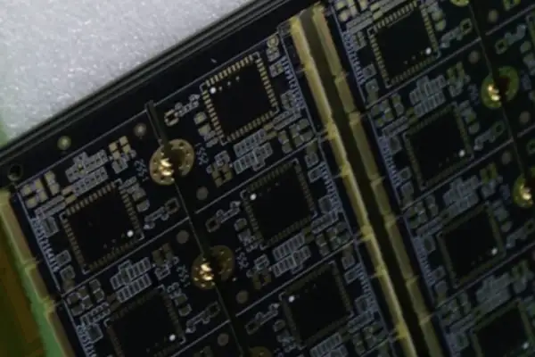
The Energy Domain Concept
The failure pattern in that project reflects a broader principle. A PCB is not a flat surface where signals coexist. It is a medium through which different categories of energy flow — categories that have fundamentally different characteristics and that interact destructively when not separated.
The control domain handles milliamp-level logic signals. It requires a stable, clean power reference and minimal noise on signal return paths. The drive domain handles ampere-level and higher currents that switch rapidly. Each switching event generates electromagnetic disturbance at multiple frequencies. The analog domain handles sensor signals that may be millivolt-level and that are entirely vulnerable to the switching noise the drive domain produces.
Placing these domains adjacent to each other without deliberate separation is equivalent to locating a reference laboratory adjacent to a forge. Physical proximity between incompatible processes degrades both. The principle that governs good layout is not distance measured in millimeters — it is the integrity of current return paths.
High-speed digital switching current must return to its source through the ground structure. If the return path is forced around a gap in the ground plane, the return current takes the available path — which may be a long loop that radiates noise or couples to adjacent sensitive circuits. A complete, uninterrupted reference ground plane is more effective than any local trace spacing adjustment.
Building the Energy Map Before Placing Components
The design sequence that prevents most mixed-signal interference problems reverses the conventional approach. Rather than beginning with component placement and then addressing noise afterward, the productive sequence starts with identifying energy domains and their supply and return requirements.
For a gateway board that integrates control logic, analog sensors, and power drive outputs, the energy map defines: a clean logic supply domain, a potentially noisy digital I/O supply domain, an isolated analog front-end supply domain, and a power output stage supply domain. Each has its own supply entry point and ground connection strategy. The domains connect at a single star point — maintaining separation while establishing a common reference.
This requires additional filtering components: magnetic beads or small resistors to establish domain boundaries at power entry, bypass capacitor networks tailored to the frequency characteristics of each domain. The additional component count and board area is modest. The alternative — a single supply rail shared across all domains — reliably produces coupling problems that are difficult to trace and expensive to fix through layout revision.
Stackup Planning for Mixed Signals
Stackup decisions for IoT gateway boards affect EMC performance more than any subsequent trace routing adjustment. The relevant principle is providing clean, low-impedance reference planes adjacent to every high-speed signal layer.
For mixed-signal systems, the stackup should provide dedicated power and ground planes for sensitive analog circuits, separate from the digital domain planes. Via routing between layers needs careful review to prevent signal current return paths from crossing between domains. The most problematic configurations occur when signal vias cross split planes — the return current must detour around the split, creating the antenna loop that radiates and couples noise.
Simulation at the stackup planning stage provides information that trace-level routing cannot recover later. Power integrity simulation validates that the target impedance of each power domain is maintained across the operating frequency range. Switching regulator noise at the analog supply entry point should be analyzed before layout begins, not discovered during functional testing.
Sensor Signal Protection in Practice
Analog sensor inputs represent the most vulnerable signals in a gateway design. The path from sensor connector to ADC input carries signals that may be at millivolt levels, with meaningful bandwidth up to tens of kilohertz. Any noise coupling that reaches this path degrades measurement accuracy.
The practical layout rules for this path are more specific than general recommendations. Symmetric, star-topology grounding concentrates the reference connection at a single point for the ADC, reference voltage source, and input amplifier. This single-point ground connects to the main analog ground plane through a relatively wide, low-inductance trace. The topology prevents ground potential differences from appearing as signal offsets.
Differential trace pairs for sensor inputs provide common-mode rejection of interference that couples equally to both conductors. The effectiveness depends on maintaining matched impedance throughout the path — including through connectors and across layer transitions. Any impedance discontinuity in a differential pair reduces the common-mode rejection that the topology is supposed to provide.
The lesson from a temperature control node that experienced persistent data drift — traced eventually to analog signal traces running adjacent to a power switching section — is that proximity violations in this area have consequences that are difficult to diagnose from functional test data. The symptoms resemble calibration drift, sensor aging, or ADC non-linearity. Identifying the actual cause requires RF-aware debugging techniques that most functional test procedures do not include.
HDI and High-Density Integration: What the Manufacturer Must Understand
IoT gateway boards increasingly incorporate dense BGA packages for communication processors, along with multi-protocol interface chips and RF modules. High-density interconnect structures — microvias, blind vias, buried vias — enable the required routing density. The manufacturing requirements for these structures are qualitatively different from standard PCB production.
Solder paste printing accuracy, reflow temperature profile control, and PCB dimensional stability during assembly all affect BGA joint quality in ways that are invisible in functional testing but predictable in field reliability. PCB dimensional variation from thermal expansion during lamination affects the accuracy of via landing pads. A manufacturer who measures and compensates for layer-specific expansion coefficients produces more consistent via placement than one who applies a fixed compensation factor.
BGA solder joint quality cannot be verified by visual inspection. Void percentage in solder balls, joint shape, and intermetallic compound layer thickness require X-ray analysis. The specification for acceptable void percentage is not standard across applications — for high-current power connections, lower void percentage is required than for low-current signal connections. A manufacturer who applies a uniform void percentage standard regardless of application has not understood the requirements.
The most useful supplier question in this context: describe how your process engineering team responds when a customer’s design produces yield problems during first article inspection. The answer distinguishes manufacturers who treat yield as a fixed characteristic of their process from those who engage with design and process interaction — which is where the actual problems live.
Supplier Engagement From the Start
The pattern that produces the most reliable IoT gateway PCBs involves manufacturing engineering participation before Gerber file submission. A capable HDI PCB manufacturer, reviewing a design in early layout stage, can identify via patterns that create manufacturing difficulty, suggest line width adjustments that improve etch consistency, and flag stackup configurations that have historically produced lamination problems.
These inputs change design decisions that are cheap to change at layout and expensive to change after production. The manufacturer who only executes final files is providing less value than the process permits. Building the relationship to include design-stage review requires more initial communication, but it is the engagement model that produces first-article success rates that make project timelines predictable.
Reliable IoT gateway performance in industrial environments requires hardware that works correctly in conditions the laboratory does not replicate. The design decisions that determine field performance — stackup architecture, energy domain separation, return path integrity, RF isolation, thermal management — are all made before the first component is placed. Getting them right requires the same integrated thinking that the gateway itself applies to the data it manages.
Many engineers focus too much on technical parameters early on and overlook
As someone who has worked in PCB outsourcing for years, I’ve found
Cramming a camera, amplifier, dual-mic array, and Wi-Fi radio into a palm-sized
- Experte für die Produktion kleiner bis mittlerer Chargen
- Hochpräzise PCB-Fertigung und automatisierte Montage
- Zuverlässiger Partner für OEM/ODM-Elektronikprojekte
Geschäftszeiten: (Mo-Sa) von 9:00 bis 18:30
Get quote, solution or any question, Andre always here to help