

HBM Memory PCB Manufacturing Challenges: How to Vet HDI and Multilayer Suppliers for Warpage, Micro-Via, and Heavy Copper Risks
Building a board around HBM is harder than the datasheet suggests. Learn
In an immersion cooling server, the PCB is not just wetted by the coolant; it lives in it. The fluid changes the dielectric environment around traces, connector pads and vias, and over months it can swell solder mask, leach plasticizers out of the laminate, drive liquid into micro-voids and weaken the copper to resin interface. These lessons come from hands-on projects: bury or compensate high-speed lines using the dielectric constant measured in the actual fluid at operating temperature, plug and cap vias, specify immersion-grade laminate and solder mask, and choose multilayer, HDI or heavy copper manufacturers by their immersion test data, cross-sections and process discipline rather than their price or label. The sections below describe each failure and fix, and a short FAQ follows at the end.
Not long ago I built a liquid-cooled server of my own, thinking that once the hardware was soaked in coolant it would be done, and the PCB step alone nearly drove me crazy. I used to think a server only has to run, so what could be hard about making a board. Then I immersed my first-version board in fluorinated liquid, ran a 112G signal, and could not capture an eye diagram at all, and only then did I realize this was far more complicated than I imagined. The problem was not in the traces I drew; I simply had no concept of what an Immersion Cooling Server PCB is: the behavior of a high-frequency signal in a liquid is a completely different world from that in air. In all my years in hardware, it was the first time I felt the default air boundary conditions in simulation software were naive.
What helped me fill that pit was a high speed PCB manufacturer, not large but with many years of focus on liquid-cooled boards. After talking, I learned that in an immersion environment the impedance of surface microstrip lines is pulled off directly by the dielectric constant of the liquid. If you follow a conventional FR4 stackup and send the board out, even if the trace length is exactly the same, the impedance measured in the oil can differ by a dozen or so ohms. Their advice to me was that, rather than struggling with simulation models to fit the coolant parameters, it is better to bury the surface high-speed lines into the inner layers from the manufacturing end, changing them into a stripline structure. That calls for multilayer board technology, and an ordinary four-layer board simply cannot hold it all. In the end I chose a multilayer PCB manufacturer and made a ten-layer board, with 112G high-speed signals on the inner layers and only low-speed control and power on the outer layers. The cost went up a notch, but the signal no longer has to wrestle with the liquid, and is instead cleaner.
Later I also stepped into a pit on backplane interconnect. In liquid-cooled chassis they use those high-pressure plug-in SFP connectors, but you will find that the pads and solder mask bridges made by a conventional PCB factory easily absorb liquid and swell after long soaking, and when the connector solder joint stress gets large, intermittent open circuits appear. Engineers who work on traditional server boards rarely notice this problem, because they never have to consider chemical compatibility. I asked several multilayer PCB suppliers, and most said they had never made immersion boards and were unwilling to take the order. In the end, through a friend I found an HDI PCB manufacturer familiar with liquid cooling processes. They used a coolant-resistant solder mask ink and also changed the plugging to a special resin, and only then did the durability of the pad area stabilize. I tried more than 200 days of soak-and-run, and the insertion and re-measured impedance basically did not drift, so at last I could sleep soundly.
From this I drew a lesson: when making a liquid-cooled server, the board factory’s industry experience matters far more than price. Give the same Gerber to a supplier that has only made ordinary server boards, and what is delivered cannot be used; whereas a team that has specially made high-reliability liquid-cooled boards will even consider copper thickness distribution, resin system and plugging material for you. When I choose a board factory now, I first check whether they have the capability of a Heavy copper PCB supplier, because liquid-cooled boards often have to use thick copper to carry large current and strong heat dissipation, with 3Oz or even 5Oz. I found a factory that can be both a Heavy copper PCB manufacturer and an HDI PCB supplier, and finally managed to reconcile the power layers with the high-speed layers. Their HDI line width can be pressed to 3mil, and the thick copper ensures the GPU power does not sag, and this one item alone filtered out most of the prototyping shops.
In the end, the most easily overlooked thing in server liquid cooling is the damp-heat aging and chemical swelling of PCB material. Quite a few peers are still using general TG 170 board material, and after soaking for a few months it delaminates and blisters, leaving the production line in a mess. I would now rather spend a bit more to find a multilayer board manufacturer that can provide complete material compatibility test data, and I dare not skimp on critical materials. It is not much of a methodology, just experience burned with my own real money: if your liquid-cooled server project does not want to die in the first year of warranty, the know-how at the board-level manufacturing step is more important than how much noise floor you tune in simulation.
I have always felt that many people imagine the effect of immersion cooling on circuit boards as far too frightening. They mention impedance collapse and signal death all the time, as if soaking a server in coolant ruins the board. The actual situation is not like that at all. I have personally handled several immersion cooling server projects, from prototyping to small batches, and the PCB sunk in the liquid lived just fine, provided that at the design stage you know whom to find to make the board, and that you do not skimp on parts like connectors.
The real trouble with an Immersion Cooling Server PCB is not what happens when liquid enters the dielectric layer but whether the multilayer board supplier you use has the ability to control batch consistency of dielectric constant. I hit a pit once: after switching to a different multilayer PCB manufacturer, with the same stackup and the same board material model, the measured impedance values that came out differed enough to make me want to smash the instrument. Only after repeatedly checking the materials did I find the problem was in the ratio of glass cloth to resin. This factory’s lamination process was not careful, which caused Dk drift. For an ordinary board this drift might be absorbed within tolerance, but in an immersion environment the liquid itself shifts the surface dielectric environment once more, and when the two errors stack up, how could the eye diagram not close? So when I pick a supplier now I additionally require the DK/DF comparison data before and after immersion, and I will not discuss it at all if they cannot meet it.
Some people also fixate on connectors, saying the coolant will swell the plastic housing and corrode the signal pins. I admit that early immersion projects did have compatibility problems, especially with EPDM sealing rings, which after long soaking really did swell like a sponge. But later we switched to an all-metal packaged product from a manufacturer specializing in high-temperature connectors and changed the seals to fluorosilicone rubber, and the problem was solved. For the transmission lines under the connector pads, I prefer to have the HDI PCB manufacturer put the differential lines directly into the inner layers, leaving only a very short stub on the surface layer, so that the dielectric influence of the liquid is reduced to nearly negligible. There is a saying that an immersion environment must use Heavy copper PCB because of fear that chemical corrosion will eat the outer copper foil, but that actually depends on the type of liquid. We used fluorinated liquid, and after five years of long-term testing, ordinary copper thickness had no problems, while on the contrary the board material provided by some heavy copper pcb suppliers developed micro-cracks after thermal cycling because the resin system was brittle. So it is not a matter of blindly going to heavy copper; you must have the manufacturer lay out the thermal stress and chemical compatibility test reports.
High-speed boards are moving fast now, and we run 112G links every day. At the start I also read those IEEE test data, such as eye height dropping 59%, and broke into a cold sweat. But looking carefully at the test conditions, most were samples sent in by multilayer PCB suppliers using standard board material, ordinary solder mask and no customization, and soaked directly, so of course the results were terrible. If you find an experienced high speed PCB manufacturer and have them optimize everything from the stackup to the chemical composition of the solder mask layer for the immersion working fluid, the result will be two different things. I have a board here that, using low-loss board material plus a special solder mask and soaked for half a year, showed a 56G PAM4 eye diagram decline of less than 8%, with the eye width almost unchanged. This shows that the so-called “link failure” is a result of inadequate engineering design and not a fatal flaw of immersion technology itself.
On compatibility, more people care about whether the board will delaminate or blow out after long soaking. This worry is quite real. I have been in contact with several factories claiming they can make immersion boards, and some did not even switch the via-plugging resin to the chemical-resistant grade, and after a few months blistering started beside the vias. If you run into that kind of factory, however much you say “strengthen testing” is useless; the root is a problem of material selection and process control. The rule I set for the team is that before outsourcing PCBs, the supplier must provide post-soak cross-sections and metallographic analysis, with particular attention to the bond between hole-wall copper and base material. Under this requirement, the ones that can supply stably are really only two or three, including an hdi pcb supplier and a heavy copper pcb manufacturer who also takes military-grade offcuts. There are no legendary stories among them; they simply do a lot of testing and have mature formulas, so on immersion projects I am not afraid of the material compatibility hurdle at all, because the risk has been blocked at the procurement threshold.
In the end, immersion cooling does not challenge the laws of physics; it challenges the engineer’s control of the supply chain. If you are still counting on your fingers how much the dielectric constant has changed, you might as well go back and check whether your PCB factory has the corresponding process discipline. One day, when you really take compatibility and signal integrity seriously and find the right supplier, a board in an immersion environment is actually more durable than under air cooling, at least you do not have to worry every day about dust and humidity aging alternately. That is my real experience, with no mysticism, all engineering details.
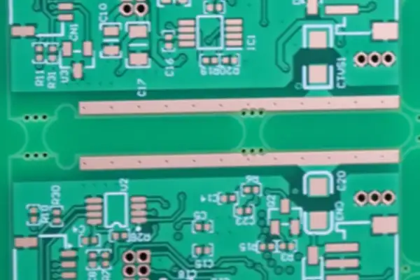
Most of the falls I have taken on immersion-cooled server projects over the past two years involve the impedance of high-speed signals. Many people think that once the PCB is soaked in coolant and the dielectric constant changes, the impedance of surface microstrip lines is certain to fall, and so the conclusion is to push every trace to the inner layers at all costs. This is not that absolute.
Last year we had a board where a height limit forced me to use only two stacked layers, and the Top layer had to run 112G PAM4. At that time I asked no fewer than five HDI PCB manufacturers, and the feedback from every one was to bury the high-speed lines, which meant adding layers and turning the process into any-layer interconnect, and the quote doubled directly. Later I met an old engineer who had worked fifteen years at a multilayer PCB supplier, and he gave me a completely different direction: do not always think about hiding; try meeting it head on in the design. You cannot change the dielectric constant of the coolant, but the line width, copper thickness and dielectric thickness in your hands are all adjustable variables. We later found a Heavy copper PCB supplier and pulled the local copper thickness to 5oz, adjusted the surface line width, and re-ran the simulation with the Dk measured in the immersed state. Impedance was basically pulled back to the target value and the return loss was controlled below -20dB. The layers and process complexity saved were far more worthwhile than the little time spent on the design change.
Of course, there is a big pit here, which is the coolant itself. The nominal dielectric constants given by different manufacturers often hover between 1.8 and 2.2, but as temperature rises this value drifts. I paid for this: I used static data measured by someone else, and after the board went online the eye diagram collapsed beyond viewing. Later I specifically found a high speed PCB manufacturer to cooperate, used their test fixture, filled it with the coolant we actually use, raised it to operating temperature and ran a vector network analyzer, obtained the real Dk and Df, and fed them back into the stackup design. After doing this, impedance control on the surface layer has no problem at all, and it also greatly saves the thermal channel design pressure of heavy copper PCB in an immersion environment, because the surface copper itself is the best heat dissipation path, and pressing all signals to the inner layers instead traps the heat density inside, which is not worth it.
The lesson from the HDI PCB supplier side was more direct. When they handle high-density routing, the filling medium of laser blind vias reacts more sensitively to coolant penetration than ordinary board material, and once residual air in the hole wall is replaced by coolant, a sudden change in local dielectric constant causes impedance spikes. This kind of detail can be found only if you have fought it out with a multilayer PCB manufacturer at the design front end. When we develop immersion boards now, from the start we take the dielectric constant and loss tangent of the coolant as design input conditions, not as a back-end compensation variable. In this way, whether it is a four-layer board or a sixteen-layer board, whether the surface layer should run high-speed signals depends entirely on the physical space of the layout and the heat dissipation needs, and not on a rigid rule that “immersion equals hiding in the inner layers.”
In the end, immersion cooling brings the PCB design not a taboo but a chance to redistribute design weight. The impedance problem is not the coolant’s fault; it is that you are still forcing the parameters from an air environment onto it. Once you straighten out this relationship, you will find that the strengths of a Heavy copper PCB manufacturer and HDI process capability can actually be magnified in immersion schemes.
I recently built an immersion-cooled server with a very dense board running 112G PAM4, and the connector impedance problem on it was far trickier than I had imagined. Once the board went into the coolant, the parasitic capacitance between the surface pads and the connector seats changed immediately, and the measured impedance fell straight from the designed ninety-odd ohms to sixty-odd, like a tripped breaker. This kind of collapse cannot be solved by fine-tuning a few line widths; you have to cover it from the stackup and material selection of the whole board.
Some people who make high-speed digital boards stare at the impedance of microstrip lines and ignore the connector node. In fact, as soon as coolant seeps into the gaps between pins and the dielectric constant is pulled up, the capacitive loading drags the impedance to the brink of collapse. I later talked with several heavy copper PCB manufacturers. Their thick copper process is indeed stable on the power layers, but for those few differential pad pairs on the signal layers, unless you re-tune the anti-pads and reference-layer openings, the signal is basically wasted. Especially in multilayer boards, when heavy copper and high-speed signals are hybrid-laminated, interlayer withstand voltage and heat dissipation get better, but impedance consistency depends heavily on the multilayer PCB manufacturer’s control of dielectric thickness and fiber-weave effects, and with a slight deviation, the return loss of the whole link cannot be held.
Interestingly, HDI boards show some advantages in this kind of immersion environment. Find a reliable hdi pcb supplier to lay out the blind and buried vias under the connector more compactly, and the parasitics of the pads can be pressed down considerably. The laser drilling precision is high, and the ground copper can be dug out right against the pad, which helps a lot to pull the impedance back. It is also not entirely the board factory’s job: the connector itself must be a model whose inter-terminal dielectric withstands fluid intrusion, and you cannot look only at the datasheet for a dry environment. I tried two connectors of the same pitch. After soaking, one had its eye height cut in half directly, while the other, because there is an air cavity protection between terminals, lost less than 5 ohms of impedance.
So now, when I meet an Immersion Cooling Server PCB project of this kind, I simply do not treat the coolant as a simple thermal medium; it is a moving dielectric layer. If the fluid is not coupled into the early simulation, all later layout adjustments are in vain. For high-speed interconnect, it is best to run a joint simulation of impedance, connector and pad parasitic models from the multilayer pcb supplier stage, otherwise when the board comes back and you put it in liquid and measure, the bit error rate soars to ten thousand ppm, and by then redoing the board burns time and money you cannot afford.
Recently I have talked a lot about immersion cooling with a few friends who build server hardware. In the whole-cabinet immersion project they just launched, problems appeared as soon as the boards were soaked in. It was not that the cooling effect was poor; the signal integrity of the PCB itself suddenly became unrecognizable. Previously we always thought that once heat was solved, everything else was a small problem, but in fact, once liquid touches the traces and pads, the whole impedance environment changes, in a way you cannot see in advance in conventional simulation.
Several multilayer board manufacturers I have been in contact with did not take immersion seriously at all at first. If you tell them the board will be used soaked in coolant, they will at most thicken the solder mask layer and change the surface finish, and never think the impedance needs to be recalculated. Differential impedance controlled to 100 ohm in ordinary air is no problem, but once the medium changes from air to long-chain fluorinated liquid, the dielectric constant is completely different, and in areas dense with local pads, capacitive coupling suddenly pulls the impedance down. We measured that on some boards, the impedance in the surface-mount pad area could drop by a dozen or so ohms after immersion, and return loss worsened to the point where 112G PAM4 simply could not run.
This actually sets a very tricky requirement for finding a reliable HDI PCB manufacturer. A board for an immersion-cooled server can no longer be accepted by the standard of an ordinary high-speed board. Especially for HDI boards, whether the laser drilling and copper fill quality of microvias will have problems under long-term hot liquid flushing is something many HDI PCB suppliers themselves are not sure of. Later I specifically found factories that make more heavy copper PCB to try, because they are more familiar with the bond between thick copper and dielectric and with thermal expansion under large current, and understand more deeply the stress in an immersion environment. But heavy copper PCB manufacturers are not omnipotent either: they can handle heat dissipation and power sections, but once the signal layers get complicated, such as when hybrid laminating high-density areas, impedance pre-compensation still has to be adjusted by a high-speed PCB factory.
Speaking of pads, this really is the most underrated weak point in an immersion environment. In air we can control impedance by removing non-functional pads and optimizing solder mask openings, but once liquid fills all the gaps, the coupling between adjacent pads is not at all what you simulated. I saw with my own eyes a board that ran a BERT test fine soaked at room temperature, but as soon as the liquid temperature rose to 40 degrees, the bit error rate took off. Analysis later showed the coupling capacitance was too sensitive to temperature, and the change in coolant viscosity made local filling uneven, so impedance fluctuation exceeded the link budget. In this scenario, all you can do is require the multilayer PCB supplier’s production line, when doing 100% impedance testing, to additionally simulate the load condition in the immersed state, instead of giving only a TDR report measured in air.
So now when I advise others on a scheme for an immersion cooling server PCB, I basically insist on several points: do not blindly trust the immunity theory from the optical module world, and for copper links you still have to honestly treat pads and connectors as impedance breakpoints and pre-compensate them; the high-speed PCB manufacturer you cooperate with should ideally be able to provide experience data directly for immersion environments, or at least be willing to do several rounds of trial boards with you; if the on-board power section carries large current, directly use the scheme of a heavy copper PCB supplier and do not force thick copper into a multilayer board, because that makes the stackup of the signal layers harder to control. These are all lessons; only after stepping in pits do you know that immersion cooling looks like a thermal design matter, yet in the end it is often the PCB that takes the blame.
I only really dove into server immersion cooling over the past year or so. Before that I thought it was nothing more than tossing the machine into coolant, and running was enough. In practice the pits on the PCB side were much deeper than I imagined, and many problems did not explode at the start; they began to fail mysteriously only after months of use.
I remember that when I first took over an immersion cooling project, I casually found a multilayer pcb supplier I was used to working with and had them make the board to conventional specifications. After two weeks of running, the board started to have trouble, either pads falling off or via impedance jumping around, and the coolant gradually clouded. Later, when I fished the board out and cut it open, I found the glass cloth and resin in the inner layers had already begun to separate, as if soaked and swollen by something. And that was only an ordinary machine room environment, with a temperature of forty-odd degrees, nowhere near extreme conditions.
Only later did I understand that in immersion cooling the whole PCB is soaked in coolant; it is not local heat dissipation but full penetration. So besides heat, chemical compatibility is what is truly deadly. Many manufacturers advertise that they can make “immersion server mainboards,” but if you ask whether their solder mask ink has been tested in fluorocarbon fluid immersion, they cannot even explain how many kinds of fluorocarbon fluid there are. Now when I talk with suppliers, I directly ask them for the solder mask adhesion, moisture absorption and dielectric constant shift data under immersion conditions, and if they cannot produce them, I do not talk further. Because of this, over these years we changed several hdi pcb manufacturers and high speed PCB manufacturers, and in the end screened out only two who had really done supporting tests.
There is another very counterintuitive point. I used to think that in an immersion environment, coolant filling the vias would actually help heat dissipation and so should be harmless. In fact the thermal expansion coefficient of the coolant differs greatly from that of copper and FR-4, and when the temperature cycles, the liquid in the vias produces great stress, especially in holes with a high aspect ratio, and over time the inner-wall copper simply cracks. So on our boards afterward, all vias must be epoxy plugged and then capped with copper, so that liquid cannot get in. This may not be so strict in conventional high-speed boards, but in immersion cooling it is a hard indicator, otherwise batch rework within half a year will kill you.
I should mention the heavy copper PCB part. Many people think using a thick copper board can withstand the high heat flux of an immersion environment, but it is actually the opposite. The greater the copper thickness, the harder it is to match Z-direction expansion with the base material, and once the coolant shocks it, the interface between copper and base material is a natural stress concentration point. We did a test on a power module: boards from a 3oz Heavy copper PCB supplier, running more than four hundred thermal cycles under immersion conditions, showed micro-cracks at the copper edges. Although they had not yet broken, such early failures are simply never seen in conventional air cooling. Later we had to reduce the copper thickness and use multilayer paralleling to share the current, and designate a multilayer pcb manufacturer able to provide an immersion-specific lamination process to make it.
HDI is different too. HDI on an immersion cooling board is used more to gain the advantage of compact layout, not simply for high speed. Because the coolant itself has a dielectric constant, after soaking in liquid the surface impedance design differs greatly from that in air. If you do not do measured calibration and make boards directly from the stackup data given by a conventional hdi pcb supplier, the signal eye diagram closes beyond viewing. We now require that at design time we must obtain the actual dielectric constant under immersion conditions and then back-calculate line width and spacing, which is equivalent to one board needing two sets of impedance control parameters, and that is quite a challenge to the process control of an hdi pcb manufacturer.
Overall, for an immersion cooling server PCB, the key is not whether it can be made but whether it can last. Many factories say they can make it, but actually you are doing the reliability verification for them. When choosing a supplier, do not look only at whether they carry the immersion cooling label; have them explain the long-term failure modes under immersion, and if they cannot produce specific interception measures, do not use them however cheap they are.
Having seen many immersion cooling deployments in the past year, I actually feel the issue of elastomers has been over-amplified. The industry keeps bringing up O-rings and rubber seals, as if one soak in coolant means the end, but it is more a matter of insufficiently careful material selection. The trouble that truly gets you called out of bed at midnight is often buried in the board you thought was the safest.
Among the several Immersion Cooling Server PCBs I have handled, almost none had a problem because an aging seal ring forced a shutdown; it was all slow corrosion and interlayer separation inside the board. Once, a 25G link had intermittent packet loss, and only after several days of investigation did we find a micro-crack at the bottom of one blind via, where coolant had been slowly pumped in during thermal cycling and the copper at the edge had been corroded black. That batch of boards still came from a not-small multilayer pcb manufacturer, using material with not-low TG, but the resin wetting of the hole wall during lamination had a dead corner, and after four months of soaking, when cut in section, the root of the blind via looked as if a knife had carved a ring around it. Since then I have been especially annoyed by schemes that give only elastomer compatibility tests at the very start. That stuff can at least be replaced when it breaks; when the inside of a board rots, you can only return the whole machine to the warehouse.
The fragility of HDI boards in an immersion environment is especially underestimated. Many hdi pcb suppliers slap their chests about how high their laser blind via fill rate is, but if you CT-scan a batch of boards, two or three out of ten have bubbles or dimpled ends in the plugged holes. Such microscopic voids may do no harm for ten years in an air-cooled environment, but once soaked in coolant, since the surface tension of the liquid is much smaller than that of air, it is only a matter of time before it drills into those cracks. Later I set a rule for myself: any hdi pcb manufacturer asked to make boards for long-term immersion must provide SEM images of blind via cross-sections of sample boards after pressurized soaking. I do not look at their shipping report; I look only at whether the hole wall and the bottom fill dielectric have separated after soaking. A few factories did three rounds without passing and finally said they could not take the order, which was honest at least.
On the multilayer board side, a multilayer pcb supplier faces a harder problem, not single-point failure but the slow drift of the dielectric performance of the whole board in the liquid. In high-speed projects I am used to choosing fixed high-speed materials, but the Dk test data given by some high speed PCB manufacturers was measured at room temperature and humidity, not soaked in the two-phase fluid. Once the liquid molecules diffuse into the resin, the loss factor can rise by 0.00-something after three months, which does not matter at low frequency, but for a 112G PAM4 signal the eye diagram closes directly. So later I would soak test coupons myself and pull S-parameters every two weeks, and only after getting the measured curve would I go and talk to the board factory: if you say it is qualified, it must be run according to the post-immersion state, and do not fob me off with standard conditions.
The situation with heavy copper boards is different again. Peers who have done high-current immersion schemes should have encountered a strange failure: the board runs perfectly in its first two months, and then suddenly an inner-layer short appears. Opening it, you find thin long gaps along the glass fiber direction at the thick copper and base material interface, coolant has seeped in, the treatment layer on the copper surface has been corroded bit by bit, and finally a high-voltage arc carbonizes it directly. I talked with an engineer at a Heavy copper PCB manufacturer, and he said that although the roughness of thick copper foil benefits bonding strength, under long liquid immersion and repeated thermal shock the stress concentration at the interface is severe, ordinary brown oxide treatment simply cannot take it, and one must use a dedicated high-temperature lamination and a special copper surface roughening process, otherwise the large copper area is a potential tear line. And many Heavy copper PCB suppliers, to save trouble, still use the standard flow, not even willing to give half an hour of extra margin on post-lamination cure time. It would be strange if such a board did not have problems when soaked.
So now when someone talks to me about immersion cooling compatibility, I seldom discuss elastomers first. More often I pull the board factory in to do a pre-launch survey together on board material, plug-hole process and lamination parameters. Because if a seal ring swells, you will sooner or later discover it and replace it; but if the PCB itself and the coolant are incompatible at the molecular level, once that failure chain starts, the cost is far beyond what replacing a few gaskets can cover.
Some time ago, while working on an immersion cooling server, I stepped into quite a few pits, and the one that gave me the biggest headache was the long-term behavior of the PCB. Most people put their energy into coolant selection, testing boiling point, flash point and conductivity at length, while ignoring what would happen to the board itself soaked in the liquid. In the early days I tried two multilayer pcb suppliers, and the four-layer boards I got back, run in silicone oil for less than three months, began to have solder mask floating up around the edges, like being pried open from the corners by something. That pry directly exposed the copper, the impedance of some differential lines drifted, and the signal eye diagrams were a mess.
Only later did I realize that compatibility is not as simple as “does it tolerate soaking.” There is a very tricky interaction between coolant and PCB material. For example, some manufacturers add plasticizers into the base material for bending resistance. Nothing happens at room temperature, but once soaked in heated fluorinated fluid, the small molecules slowly dissolve out, and not only does the liquid darken in color, the dielectric constant also drifts quietly. This kind of change is insidious: it does not immediately bring the system down, but makes your high-speed link good and bad by turns, and tracing the root cause is extremely tormenting. Because of such hidden contamination I wastefully replaced optical modules twice, and in the end found that precipitates from the board material were the culprit.
Now, when selecting an hdi pcb supplier, I lay the immersion environment straight out and ask whether they have done peel strength tests after high-temperature aging and whether the dielectric constant has been measured after 1000 hours of liquid immersion. Some multilayer pcb manufacturers simply do not understand this requirement and only repeat the numbers on the datasheet, and I pass on them directly. High-speed board manufacturers are a bit more sensitive. I dealt with a high speed PCB manufacturer who told me directly that some low-loss materials easily absorb moisture and swell in liquid cooling, and suggested switching to a different resin system, along with changing the surface treatment of microstrip lines to a more passivated coating. That kind of conversation is valuable.
For large current areas I basically cooperate with heavy copper PCB suppliers, because the cross-section to surface area ratio of thick copper traces is larger, the corrosion rate is relatively low, and the heat conduction path is more direct. But you cannot take it for granted: once a heavy copper PCB manufacturer I used had a solder mask ink with insufficient chemical resistance, which after long soaking in coolant became like soft rubber skin, and the touch of the whole board when taken apart was eerie. Afterward everything was changed to the immersion-specific high-temperature-cured solder mask, and only then was the problem solved.
In the end, the most easily underestimated thing about immersion cooling server PCBs is the time dimension. Passing a single soak test is nothing special; you have to run it continuously in the system and periodically sample and analyze the ions and organic contaminants in the coolant. My practice now is that however urgent the board order is, I make the manufacturer provide a material leachables report, or send it to a third party for GC-MS analysis myself. If this stack compatibility is not laid out clearly early on, the maintenance cost afterward will definitely make you wince. Cooperating with a reliable hdi pcb manufacturer, moving this layer of risk forward to the design stage, is much more effective than adding filters or changing coolant afterward.
I came into contact with immersion cooling about three years ago. A project at the time was converting a batch of high-density servers to immersion, and at first everyone stared at the coolant and the sealing structure, and nobody cared what would happen to the PCB soaked in the liquid. When the first round of prototypes came back and ran for less than two hundred hours, with blistering at the board edges and micro-cracks in the BGA solder joints, the boards were basically scrapped, and only then did someone remember board-level reliability.
The biggest difference between immersion cooling and air cooling is not the on-paper figure for heat dissipation capability. A temperature jump of nearly twenty degrees per minute is a different physical environment altogether for a PCB. In the air-cooling era you could tough it out with experience and standard test procedures, but in an immersion tank, the Z-axis expansion coefficient of the board material, the liquid resistance of the resin system, even the adhesion of the copper foil are all put under a magnifying glass. When I reviewed that project afterward, I found that the multilayer pcb manufacturer we used at the time had simply copied the process and stackup of traditional data center boards and had not even raised separate thermal cycling verification conditions for an immersion environment.
After going around a big circle I found that, for an immersion cooling server PCB, the manufacturer’s control over the thermal history of the material matters more than anything. It is not that any multilayer pcb supplier can solve the problem by taking a high-Tg board material. The plasticizing effect of the liquid quietly lowers the glass transition temperature of the resin, and over long soaking, the thermal stress margin you calculated can be directly broken through. Boards that should have passed 1000 thermal cycles from -40 to 125 degrees, after being soaked in liquid and run through the same temperature profile, can have their delamination point arrive several hundred cycles earlier.
Later I slowly formed a habit: before discussing an immersion project, I first ask the hdi pcb supplier I work with three questions. Do you have measured data on peel strength decay after long-term soaking in dielectric fluid? Can you provide comparison thermal cycling reports for the same batch of material in immersion and air-cooled environments? And for the dielectric constant shift of the high-speed signal traces, were the original parameters used in your modeling measured in room-temperature air, or measured after soaking in the target liquid for hundreds of hours? Of ten manufacturers, there may not be two who can answer. Many hdi pcb manufacturers say they can make high layer counts and control impedance, but when asked for accelerated aging data in an immersion environment, they show you the datasheet of general board material, which is not the same thing at all.
The manufacturers who make heavy copper pcb are, in this area, naturally somewhat more sensitive. Because thick copper boards themselves must bear severe thermal and electrical stress under large current, much of their process control over copper thickness distribution, via fill and interlayer bonding can be transferred directly to an immersion environment. For a while I specifically talked with heavy copper pcb suppliers about immersion schemes and found that they understand how a board will deform under thermal shock and where stress concentrates at weak interfaces, and they are much easier to communicate with than factories that make only consumer multilayer boards. Of course, the process capability of every factory differs enormously, and not every heavy copper pcb manufacturer really understands immersion; you have to try them one by one yourself.
The high speed pcb manufacturer side is another story. The dielectric constant of immersion liquid is considerably larger than that of air, which directly affects the impedance of microstrip and stripline and the signal propagation delay. A 112G PAM4 link that could run stably in an air-cooled environment collapsed its eye diagram in the immersion tank, and it took two days to find that the dielectric parameters the manufacturer used to calculate my line width had never taken the influence of the fluid into account. So now whenever high-speed signals run on an immersion board, I require the board factory to bring the liquid parameters into the stackup simulation, and to state the valid temperature range and aging offset of these parameters, otherwise production cannot be released.
The thermal management dividend of immersion cooling is visible to everyone, but the traditional approach of treating the PCB as an isolated component certainly will not work. From board material selection to lamination process, to solder mask and surface finish, a board must be reconsidered in that liquid tank under constant thermal cycling. Whether it is the multilayer pcb supplier or the hdi pcb supplier you choose, they must be willing to face these troublesome matters with you, not just quote you a layer count and minimum line width and spacing and be done.
A few years ago I handled an immersion cooling project, and at the time I thought, since the coolant does not conduct electricity, a PCB soaked in it should be easier, and yet the connectors alone cost me three months. It was not the kind of thing where large current burns something out, but signals that drifted in the middle of the night, with the PAM4 eye diagram good and bad by turns. After much struggle I found the coolant had seeped along the tiny gaps in the connector shell, and with alternating hot and cold, whatever inside could expand expanded and whatever could precipitate precipitated, and the normal force at the contact points changed. Since then, when I choose connectors, I always soak samples in the coolant, run dozens of rounds of thermal shock, and then look at contact resistance and high-frequency return loss. Looking only at data from an air-cooled environment is the same as not looking at all.
For this kind of project, the PCB itself is also not something any factory that can make multilayer boards can handle. The first multilayer pcb manufacturer we used had through-hole wall quality that was fine in a dry environment, but after long soaking the difference in water absorption between glass fiber and resin was magnified, and tiny changes in hole diameter shifted the impedance of high-speed differential pairs. Later we switched to an hdi pcb supplier specializing in high-speed hybrid lamination, who used a lower-loss base material, changed the structure of the laser blind vias, and also changed the plugging resin to a low-expansion formula, and only then was the fluctuation of the link pressed down. For boards with high current density, such as power areas that rely on copper fill for heat conduction, I prefer to find a Heavy copper PCB manufacturer to directly build thick copper inner layers plus embedded copper coins, which is far more reliable than attaching heat sinks later. And such process details are generally things an ordinary multilayer pcb supplier will not bring up proactively; you have to chase them with questions yourself.
There is also a pit it is easy to be dragged into: many people feel that soaked in an insulating coolant, the signal shielding requirement for the PCB can be reduced. In fact it is just the opposite. The dielectric constant of the coolant differs from that of air, and the liquid medium near the traces changes the electromagnetic field distribution, especially for outer-layer microstrip lines, where the field on the former air side is suddenly pulled askew and the characteristic impedance and phase velocity all change. So now whenever I design an Immersion Cooling Server PCB, I always require the High speed PCB manufacturer to re-extract the parasitic parameters of the entire link, and the stackup of the earlier air-cooled version cannot be reused. If this step is skipped, you will tune the bit error rate in the machine room until you doubt your life.
In the end, immersion cooling is not changing an air-cooled chassis into a liquid pool; the PCB in it is a different physical system. The interactions of coolant with connectors, board material, solder mask and copper foil are long-term and dynamic. When I look at a board factory touting itself as an hdi pcb manufacturer or a Heavy copper PCB supplier now, I do not care much about the title; I care more about whether they have a group of people who have really soaked and tested boards in coolant, and whether they have accumulated the ability to work backward from failed samples to design boundaries. In this trade, judgment piled up from experience is worth far more than a parameter table.
What gives me the biggest headache in server immersion cooling is not heat dissipation efficiency but that PCB soaked in the coolant every day. Many people say all the time that the dielectric constant of the coolant will upset impedance, the eye diagram will be a mess, and FEC cannot keep up, which sounds quite scary, but if you bury the key high-speed signals in the inner layers and then cooperate with a reliable hdi pcb manufacturer on the stackup, the little loss on the surface layer is not a problem at all. The real place to capsize is the board material itself. In one project I used ordinary high-Tg FR-4 and made no liquid resistance requirement to the multilayer pcb supplier, and in less than four months the board edges began to absorb liquid and swell, the solder mask wrinkled, and the microstrip impedance drifted until it could not be looked at. Later I switched to a multilayer pcb manufacturer that had specifically done immersion tests, using low-moisture-absorption base material, a chemical-resistant solder mask and ENIG surface finish, and only then did those strange attenuation problems calm down.
On choosing suppliers, I have actually worked out a bit of experience. For an Immersion Cooling Server PCB, do not be led by the unit price; look at whether the other side has genuinely done real work on high-density interconnect and heavy copper processes. Because this kind of board often needs thick copper for the power section to carry large current, while the signal traces must squeeze into thinner interlayer spaces and fan out through HDI blind and buried vias. An ordinary multilayer board factory cannot handle this kind of hybrid structure, and you need a factory that is both a heavy copper PCB manufacturer and an hdi pcb supplier, preferably with a high-speed signal processing background as well. My habit now is to first ask whether they have run CAF testing and thermal shock in at least seven or eight kinds of coolants, and those who have not heard of the ODCC material recommendations can basically be skipped.
On signal integrity, my view is that you should not put all your hope on FEC. Forward error correction can indeed provide a backstop, but if the channel quality of your board itself is a mess and you rely only on error correction to tough it out, the system margin is eaten completely. So in the Layout I would rather have the high speed PCB manufacturer help me press the outer-layer fan-out to the shortest, with connectors on the back side, and do impedance pre-compensation directly at the AC coupling pads. As for the dielectric environment effect brought by the coolant, just treat it as a known stackup parameter and bring it in; it is not as mysterious as the internet says. On the contrary, the spring contacts and seal rings of connectors, which harden and deform after long soaking, are a bigger pit than a few dB of loss, and a slightly greedy wrong choice of material at selection will show you a rude surprise in a month or two.
On several immersion-cooled server projects I have handled over the past two years, dealing with PCB manufacturers, the biggest pit has in fact not been design theory but actual manufacturing level. Many people start by agonizing over the dielectric constant of the coolant and fight to the death over impedance compensation of surface microstrip lines, while ignoring the most basic links, via consistency and sealing process. I can understand why many articles rank vias last in priority: in simulation the skin effect does make the signal travel along the outside of the hole wall, and the impedance difference looks small. But that is the ideal condition. On a real production line, the lamination deviation of a multilayer pcb supplier, the depth tolerance of back drilling, and the expansion coefficient of the plugging material can casually make via impedance drift by several ohms. Let high-speed signals soak in coolant every day, add this small drift on top of the reflection from the connector, and in a 112G PAM4 eye diagram it simply cannot hide.
I have one especially deep lesson. At that time, to save effort, I directly reused the board scheme from an earlier air-cooled server, only pre-compensating the surface microstrip lines, left the via areas almost untouched, and found an ordinary multilayer pcb manufacturer to prototype. The initial board test was quite beautiful, but after two months of immersion aging, micro-cracks began to appear in the pads near the SFP connector, and the via impedance of several differential pairs dropped from 100Ω all the way to around 92Ω. When we took it apart, the coolant had already seeped along tiny cracks in the hole wall into the inner layers and had corroded exactly that segment of the signal path. This was completely different from the clean data in simulation. We then urgently switched to a dedicated high speed PCB manufacturer to re-prototype, forcing epoxy plugging plus copper capping and controlling back-drill accuracy within ±25μm, and only then did the impedance stabilize. This also made me reconsider the weight of vias in an immersion environment: they may not be the most sensitive node in design, but they are definitely the place in manufacturing most prone to batch-wide capsizing.
Connector and pad problems, on the other hand, can be solved by routing strategy and choosing the right process. For example, for the pads under a BGA, when revising the board we compressed the surface fan-out to the shortest, and wherever we could avoid a microstrip line we did, burying everything into inner-layer striplines. This adjustment pressed back considerably the 5-6Ω of low impedance the coolant takes away. But it also brings a hidden requirement: the transition handling of heavy copper PCB. Because immersion servers carry large current mostly through inner-layer thick copper, if you casually find a Heavy copper PCB supplier, it may well use a large copper plane to transition directly to the fine pads of the signal layer, and the abrupt copper thickness change causes a sharp local impedance dip, and after the connector is attached the return loss blows up at once. We measured a batch of samples where the impedance difference in the pad area was nearly 11Ω, which is more violent than the dielectric environment change alone. So afterward when ordering boards, we locked in a Heavy copper PCB manufacturer able to handle both thick copper and signal layers, and forced them to do a stepped thinning at the copper thickness transition, and only then was the pad impedance fluctuation pressed within 3Ω.
Now on the HDI side. Many people think immersion cooling has no need for HDI, feeling that once heat dissipation is solved, a conventional multilayer board can handle it. But actually the trace density on server mainboards keeps rising, with differential pairs easily numbering several hundred, and without laser drilling it simply cannot satisfy length-matching constraints. An hdi pcb manufacturer I used drilled buried vias directly under the connector pads with laser, the via stub was almost zero, the delay skew of the differential pairs was greatly reduced compared with the conventional through-hole scheme, and the width of the 112G eye was even better than I estimated in simulation. This also means that when I choose an hdi pcb supplier now, I must see their long-term thermal stress test data for immersion environments, and not just be fobbed off with a dielectric constant compensation table.
Overall, my view now differs from the line of thinking that ranks vias lower in priority. For an Immersion Cooling Server PCB, the multilayer pcb manufacturer you find must be able to control the impedance continuity among vias, pads and connectors as a whole, watching everything from plugging material to thick copper transition. If you put all your hope on εr compensation in simulation software, then as soon as the production line loosens a bit, vias are the first short plank of the barrel to be exposed.
There is a rather counterintuitive feeling in this line of liquid-cooled servers: everyone spends much effort discussing compatibility between coolant and PCB base material, as if choosing a “universal compatibility” coolant settled everything, but what really keeps me awake is never the coolant itself but the process residue from the board factory. In an immersion environment, flux residue and micro-etch remnants hidden in via corners and in the underfill gaps of BGAs are more dangerous than any parameter in the coolant’s chemical analysis report. We once tested the product of a multilayer board supplier whose base material and coolant compatibility showed no problem, but once powered up and running, after two weeks the dielectric constant drifted beyond viewing. When we took it apart, we found the inner copper surface treatment had not been cleaned off, and long soaking in the coolant pulled those ionic residues out bit by bit, and formed a micro-battery effect right inside the board. After that I insisted on one rule: the multilayer board manufacturer you choose must be able to explain their cleaning process to you transparently, and it is not enough that the factory withstand voltage test passed, because this directly decides whether your server will be stable or intermittently haunted over the coming year.
Speaking of board factories, there are actually not many in China that can make this kind of board well, and factories at different positioning differ enormously. Many people think an immersion cooling server PCB is just an ordinary server board thrown into liquid, but in fact you have to reconsider things starting from material selection. For example, with heavy copper board suppliers, many provide thick copper boards for power use, but in a liquid-cooled environment, once the current density gets large, the risk of cathodic filament corrosion is completely different, and you must check whether they have done dedicated solder mask adhesion and copper surface passivation treatment for liquid environments. I stepped into plenty of pits: some heavy copper PCB manufacturers claim the copper thickness can reach 10 ounces, but soaked in coolant and thermally cycled to 600 times, the copper blistered, because they never thought that coolant molecules penetrate the copper and base material interface far faster than air. Later in screening partners, I built a small test bench myself and threw those factories that claim they can make high-speed PCB or HDI boards directly into the coolant we were evaluating, flipping them repeatedly between -40 and 125 degrees, and did not let them out without 1000 cycles, to see how much the impedance drifted and whether there were micro-cracks. Nobody should fob me off with dry-state data from a datasheet.
I am especially picky about HDI. Server and switch boards are getting thinner, with line width and spacing shrinking below 3mil, and many HDI PCB suppliers say they are high-end process, but the reliability test of their microstructure by an immersion environment has only just begun. Laser-drilled sidewall roughness and the moisture expansion coefficient of plugging resin, which could be overlooked in the air-cooling era, all turn into time bombs in coolant. Once I received a batch of HDI boards that, after SMT, showed regular collapse in the signal eye diagram. After going around the whole circle, we finally found that the resin inside the microblind vias had swollen in the coolant and forcibly cracked the hole copper, cutting off the signal return path. This incident made me realize that boards for immersion cooling simply cannot be accepted by simply continuing traditional IPC standards; you must align test conditions with the HDI board manufacturer from scratch, treating the coolant as a constantly present stress source and not water splashed on by accident.
Now many people like to use simulation tools for pre-emphasis and impedance compensation when talking about high-speed PCB design, but under immersion there is a physical fact that is easily overlooked: the dielectric constant of the coolant is higher than that of air, and its rate of change differs at different temperatures. This means the electric field distribution on the surface of signal lines changes entirely, and the eye-height margin previously recovered by FEC may hit the wall directly in the new dielectric environment. If a high-speed PCB manufacturer gives you only Dk/Df data at the FR4 or M6 level and has not considered tests in a liquid-wetted state, the differential impedance deviation of the board that comes back will make you doubt your life. My habit now is that, whichever multilayer board supplier I cooperate with, at the early sample stage I always require them to produce two sets of impedance coupons, one bare at room temperature and the other fully soaked in the coolant we specify and measured after thermal stress, and if the difference between the two exceeds 5%, I change factories directly.
Building a board around HBM is harder than the datasheet suggests. Learn
Gas leak detector PCBs drift from humidity leakage, residue, and laminate variation,
At 77GHz, dielectric thickness drift, PTFE and FR-4 hybrid lamination, and supply
- Experte für die Produktion kleiner bis mittlerer Chargen
- Hochpräzise PCB-Fertigung und automatisierte Montage
- Zuverlässiger Partner für OEM/ODM-Elektronikprojekte
Geschäftszeiten: (Mo-Sa) von 9:00 bis 18:30
Get quote, solution or any question, Andre always here to help