
Fiber Optic Equipment PCB: Mastering High-Speed Signal Integrity & Multi-Layer Challenges
When data centers upgrade their GPUs, the real bottleneck often hides in
Having worked in the high-frequency PCB industry for so many years, I increasingly feel that choosing the right partner is more important than anything else. Some companies like to frequently change PCB suppliers to reduce prices or pursue short-term gains, but I believe this is precisely the biggest risk. High-frequency signals are extremely sensitive to board characteristics and processing precision.
I have seen too many product consistency disasters caused by unstable suppliers. For example, once we switched suppliers at the last minute to make a batch of 77GHz radar boards, and the resulting VSWR of the entire batch was abysmal. Later investigation revealed that the different manufacturers had completely different understandings of the PTFE bonding process. This subtle difference might not be noticeable in low-frequency boards, but it’s fatal in the high-frequency field.
Truly reliable high-frequency PCB manufacturing service providers don’t stop at the order level. They proactively discuss technology roadmaps for the next two to three years and even prepare samples of new materials in advance. I remember a supplier we’d worked with for many years had already started testing lower-loss hydrocarbon ceramic substrates before we even formally submitted our requirements. This forward-looking approach allows our product iterations to always be one step ahead.
There’s a misconception in the industry that having multiple alternative suppliers reduces risk. However, the special characteristic of high-frequency PCBs is that process know-how requires long-term accumulation. We once compared three suppliers making the same multilayer hybrid laminate; the one we’d worked with the longest achieved a 95% first-pass yield, while the new supplier couldn’t even maintain stable impedance control. This isn’t a difference in equipment; it’s a matter of experience.
Of course, building a long-term relationship doesn’t mean unconditionally compromising. We regularly audit our suppliers’ key process capabilities, such as the calibration records of their microwave anechoic chambers and the parameter stability of their plasma descaling. However, these checks are more like a health check report for mutual growth than a trial. Last time, after discovering room for improvement in their phase testing, engineers from both sides spent three days together in the lab, ultimately reducing the test dispersion by 30%.
Ultimately, high-frequency PCB procurement isn’t a simple buying and selling transaction; it’s more like jointly building a technological moat. When suppliers understand your product plans for the next five years, they dare to invest millions in equipment for process pre-research; when you include them in the early stages of R&D,
many design pitfalls are avoided at the design stage.
The cost of this deep partnership might be a 5%-8% higher unit price than the market average, but compared to the customer complaints caused by performance fluctuations after product launch, this investment is far more worthwhile.
Recently, we’ve been working on terahertz band array antenna boards, and a supplier we’ve been cooperating with for ten years has directly sent engineers to our factory to participate in the design review. This kind of tacit understanding cannot be cultivated through tender documents alone.
Sometimes, looking at the stable 140GHz testing system running in the lab, I feel like this isn’t a client-supplier relationship, but more like a mountaineering team climbing the Mount Everest of technology together.
After all, in the high-frequency field, no one can reach the finish line alone.
I’ve always found the field of high-frequency PCBs particularly interesting. Many people think it’s just about routinely designing circuit boards. That’s not the case at all. Last year, our team worked on a millimeter-wave radar project. We contacted several suppliers for prototypes. We found that even though they were all providing high-frequency PCB manufacturing services, the results were vastly different.
One supplier’s board looked fine at first glance. But it immediately showed its flaws on the testing bench—the signal attenuation was severe. We later discovered that they were using too ordinary dielectric materials. They simply couldn’t withstand the losses in a high-frequency environment. This experience taught me a lesson: you can’t just look at the numbers on the quote when choosing a PCB supplier.
A truly reliable high-frequency PCB manufacturer will discuss material properties with you. They will proactively ask what frequency range your application requires. They understand how delicate millimeter-wave signals are. Even the surface roughness of the board material can affect the final performance.
The most professional approach I’ve seen is for suppliers to demonstrate the differences between different materials on-site using a vector network analyzer. That kind of intuitive data comparison is more effective than any brochure.
Now, many customers immediately ask for a lower price. But high-frequency circuits are not something you can cut corners on. Saving a few dollars on board material might cost you tens of thousands more in debugging later.
A good high-frequency PCB should act as an invisible assistant, silently supporting the entire system, not becoming the bottleneck.
The factory we later partnered with had a unique characteristic: their engineers were extremely meticulous, repeatedly checking whether our designs considered heat dissipation and mechanical stress because they understood that the heat generated by millimeter-wave devices directly affects stability.
This responsible attitude is the most valuable quality in the high-frequency field. After all, nobody wants their product to fail at a critical moment because of a seemingly insignificant circuit board, right?
Speaking of choosing a high-frequency PCB manufacturer, I recently looked at several suppliers for my company and found that simply looking at brochures is not enough. Some factories make grandiose claims, but they can’t even manage basic material storage.
I remember visiting one factory once; their workshop was piled high with PTFE substrate, without even a thermometer or hygrometer. This material is extremely sensitive to humidity; even slight moisture significantly reduces its performance. I directly asked the manager, “Do you even have a temperature- and humidity-controlled warehouse?” He stammered and couldn’t answer for a long time.
Actually, judging a factory’s reliability hinges on their attitude towards details. For example, the drilling process for ordinary PCBs and high-frequency PCBs is completely different. One small factory, to save costs, actually used ordinary drill bits to process high-frequency boards, resulting in hole wall roughness that didn’t meet requirements at all. Later, we specifically inspected their plasma processing equipment; the machines were new, but the operators couldn’t even explain the basic parameters clearly.
What troubles me most is the testing process. Many manufacturers claim to have network analyzers, but when asked to produce recent test reports, they make all sorts of excuses. Once, I encountered a supplier whose equipment was imported, but the calibration certificate had expired six months ago, and nobody seemed to care. If they can’t even manage basic management, who would dare entrust orders to them?
Now, I’m much more cautious when dealing with suppliers. For example, I ask for their impedance test data from the last three months to see if there’s significant fluctuation. I also deliberately ask about technical details, such as parameter adjustments when mixing materials with different dielectric constants. Truly professional engineers answer fluently, while those with poor skills immediately give themselves away.
Choosing a supplier is like finding a partner; you can’t judge a book by its cover. You need to understand their work habits. Sometimes a small detail can reveal the professionalism of the entire team. For example, I once saw a manufacturer mixing different batches of solder resist ink; I immediately turned away from that poorly managed factory.
Ultimately, you can’t just compare prices when choosing a high-frequency PCB manufacturer. Some small factories offer cheap quotes, but if quality issues arise later, the rework costs are actually higher. I’d rather spend a little more money to find a reliable one, at least I can sleep soundly at night.
I’ve recently been in contact with two new suppliers and plan to visit their labs next week. This time, I need to focus on their failure analysis capabilities. Last time, a project was delayed because the manufacturer couldn’t find the root cause of the problem.
By the way, if you’ve been in this industry, you’ve probably encountered even stranger things, right? Sometimes it feels like this industry is incredibly complex; every step can be a trap.
However, good manufacturers do exist. The one I visited last week was quite a surprise. Their technical director personally showed me the production line, explaining every process parameter clearly. Manufacturers who are so dedicated are becoming increasingly rare.
So my advice is: don’t rush into a decision! Visit several companies!
Over the years of making high-frequency boards, I’ve noticed an interesting phenomenon—many manufacturers boast about their high-frequency capabilities, but when you actually send them the design drawings, they can’t even guarantee basic signal integrity. Once, I met a customer who makes radar antennas, and he asked me to compare samples from two suppliers. The first company’s test report was just a thin sheet of paper, with no data except for a certificate of conformity; the second company attached a full twelve pages of spectral analysis curves, even including environmental temperature and humidity records. This difference isn’t about equipment; it’s about attitude.
Actually, there’s a very simple way to judge the reliability of high-frequency PCB manufacturing services—see if they dare to show you their testing environment. Last year, I visited a small factory in Shenzhen where their vector network analyzer was placed right next to the production line, and workers adjusted parameters directly on-site during impedance matching. Although the factory was a bit old, the engineers could easily retrieve calibration records from three months ago. Conversely, some companies claiming to have Class 10,000 cleanrooms would take three days to get a dielectric constant verification report.
I pay particular attention to the board material processing stage. I’ve seen too many factories fail due to the immersion gold process—either nickel layer corrosion or uncontrolled phosphorus content, resulting in black spots on the boards after only six months. A supplier I’ve worked with for many years is quite clever in this regard; they perform an additional micro-etching treatment before immersion gold, which, although more expensive, maintains a yield rate consistently above 98%. This kind of attention to detail is more valuable than buying a lot of high-end equipment.
There’s a misconception in the industry that affording 110GHz equipment equates to mastering high-frequency technology. But the truly crucial elements are often the most fundamental, such as the impact of fiberglass cloth weaving direction on dielectric constant, or the control of prepreg flowability. I remember once helping a telecommunications company inspect a batch of millimeter-wave boards and discovering a problem in a very subtle place: the press temperature profile was set too aggressively, causing microscopic bubbles in the dielectric layer. This kind of hidden danger simply cannot be detected through later testing.
Ultimately, choosing a high-frequency PCB supplier is like finding a barber; looking at how many certificates the shop displays is useless. The key is whether they understand what you need. I recently met a satellite antenna team, and they were most satisfied with a small factory with only twenty people—because the engineers there proactively suggested changing the transmission line corners to rounded transitions and even helped recalculate the phase compensation values. This kind of collaboration based on practical experience is more valuable than any certification.
If you’re evaluating suppliers, try intentionally leaving a small flaw in your design to test their reaction. A reliable team will point out the problem during engineering reviews, not just manufacture according to the drawings. After all, true high-frequency manufacturing services shouldn’t be a passive production line that passively accepts orders, but a technical partner that works with you to solve electromagnetic compatibility issues.
Having worked in this industry for many years, I’ve noticed an interesting phenomenon: many people instinctively think that high-frequency PCBs must be from suppliers with the most advanced equipment. However, this isn’t always the case. Of course, I’m not saying equipment isn’t important, but we need to consider our actual needs. Sometimes, it’s unnecessary to excessively pursue the highest-end configurations.
Take a project we did before, for example. It was a board used in a wireless base station. The frequency requirement wasn’t particularly high, around 6GHz. We chose a mid-sized supplier. They didn’t have those particularly expensive vector network analyzers, but their High Frequency PCB manufacturing… Services is particularly experienced in handling PTFE materials. You know, while PTFE has excellent properties, it’s quite difficult to process, especially in drilling and surface treatment. This factory uses a clever method; they achieve excellent results by adjusting process parameters instead of simply relying on high-end equipment. After the boards are manufactured, we send them to a third-party laboratory for testing, and all indicators meet the requirements, yet the cost is nearly 30% lower than hiring a top-tier supplier.
I’ve seen too many teams immediately look for manufacturers with full millimeter-wave testing capabilities, often ending up spending a lot of money on unnecessary functions. High-frequency board manufacturing does require professional technical support, but the key is to match it to your specific application scenario. For example, if your product is mainly used in the sub-10GHz frequency band, then the requirements for testing equipment can be appropriately relaxed; in fact, it should be more… Focusing on a manufacturer’s practical experience in material handling, especially for specialized materials like PTFE, is crucial. Often, the problem isn’t in the design, but rather in the insufficient understanding of material properties during manufacturing.
I once visited a small PCB factory. While they lacked the sophisticated testing equipment that some manufacturers boast, their engineers possessed a deep understanding of high-frequency signals. They could diagnose potential board problems through simple impedance testing combined with years of experience. This experience-based judgment is sometimes more flexible and effective than relying solely on instruments. Of course, this doesn’t mean we can ignore basic quality control; rather, it means that when choosing a supplier, we should comprehensively evaluate their overall capabilities rather than just focusing on hardware specifications.
I think there’s a misconception in the industry: overemphasizing equipment sophistication while neglecting the actual technical capabilities of engineers. A good high-frequency PCB manufacturing services provider should find the optimal balance between technology and cost, offering the most suitable solutions based on the client’s specific needs, rather than simply pushing their most expensive services. This is true customer-centricity.
I’ve seen many people fall into a trap when choosing high-frequency circuit board manufacturing services—overemphasizing seemingly impressive technical parameters. In reality, success often hinges on the most basic details. Take copper foil as an example. Many people think that simply choosing a material labeled as having low roughness is enough.
I remember last year a client who manufactures communication equipment used top-grade rolled copper foil in the sample stage, with excellent specifications. However, during mass production, to save costs, they secretly switched to ordinary electrolytic copper foil. The slightly lower surface roughness caused the entire batch of products to completely collapse in signal integrity at high frequencies. This seemingly minor change can have a chain reaction in practical applications. For example, in the millimeter-wave band, a rough copper foil surface increases skin effect loss, causing a sharp increase in signal attenuation of 3-5 dB. More seriously, the uneven surface structure can cause impedance abrupt changes, resulting in standing wave reflection problems.
Now, when I work on projects, I pay special attention to tracking the use of materials throughout the entire process. During each acceptance test, I randomly sample substrate sections and use a microscope to check the surface condition of the copper foil. Once, I discovered that the supplier had over-processed the etching process; although the circuit precision met the standards, it damaged the carefully selected low-profile copper foil surface structure. This kind of hidden problem is completely invisible in routine testing and only becomes apparent during high-frequency testing. We later introduced a surface profilometer for quantitative monitoring, requiring the copper foil Rz value to be controlled within 1 micrometer.
Speaking of testing, I think many manufacturers oversimplify the issue. Verifying the performance of high-frequency PCBs isn’t as simple as measuring a few points with a network analyzer. It requires establishing a complete database to compare the full-frequency performance of different batches of products. Our team has developed a habit: retaining samples from each batch for accelerated aging testing, and retesting key parameters three months later. We once used this method to discover the performance degradation trend of the dielectric material under high and low temperature cycling. Specifically, after 200 cycles from -40℃ to 85℃, the board’s Dk value drifted by more than 2%, a fatal flaw for phase-sensitive applications.
Choosing a high-frequency PCB manufacturing service is more like finding a partner. Just looking at the equipment list isn’t enough; you need to examine their attention to detail. I particularly value whether a supplier’s engineering team is willing to spend time understanding the product’s application scenario—for example, whether the board is used in a base station or automotive radar, and the temperature range of the operating environment. These factors all influence material selection and process design. For example, automotive radar boards prioritize high-Tg materials with a TG value greater than 170℃, while base station equipment requires attention to stability under long-term humid and hot environments.
A recent lesson was quite profound: a supplier’s process documentation was incredibly detailed, but in actual production, they shortened the lamination time to meet deadlines. As a result, the dielectric constant stability of the board material failed to meet standards, leading to phase inconsistencies in batches of products at different temperatures. This incident made me realize that even the best technical solutions require strict process control for successful implementation. We now require key processes to be equipped with real-time monitoring systems; for example, the lamination process records over 200 parameters, including temperature and pressure curves.
Ultimately, high-frequency circuit board manufacturing is a continuous balancing act. It requires finding the optimal balance between material costs, process complexity, and performance requirements. Sometimes, choosing slightly more expensive materials can reduce overall risk, as subsequent repair costs may far exceed the initial investment. For example, while the RO4350B is 30% more expensive than the standard FR4, its stable Dk/Df characteristics avoid the time-consuming process of repeatedly adjusting the matching circuit later.
When evaluating suppliers, I always ask two questions: How do you guarantee the performance consistency of each board in mass production? Do you have a complete traceability mechanism in case of anomalies? The answers often reflect the true level of the company. Excellent suppliers will demonstrate their SPC statistical process control charts and a complete traceability system from raw material batch numbers to parameters of each process step.
Ultimately, there are no shortcuts in this industry. Only by doing every step thoroughly and meticulously can you deliver reliable high-frequency PCB products. Like the 77GHz automotive radar board we recently made, the impedance matching alone underwent six iterations of design optimization before finally achieving a VSWR of less than 1.5 across the entire frequency band. This meticulous attitude is the true cornerstone of success in high-frequency circuits.
Over the years of making high-frequency boards, I’ve increasingly felt that this isn’t about how cutting-edge the technology is, but rather the relentless pursuit of detail. Many people think that finding a manufacturer that provides high-frequency PCB manufacturing services is enough, but it’s much more than that. Once, we encountered a project where the signal was consistently unstable in a certain frequency band. After repeated checks, we discovered that the problem stemmed from uneven solder mask thickness, causing minute capacitance variations. This issue wouldn’t occur on low-frequency boards, but it becomes fatal in high-frequency environments.
Material selection is just the beginning; the real challenge lies in the compatibility between different materials. For example, when PTFE and FR4 are mixed, the thermal expansion coefficients of the two materials differ significantly. Even slight deviations in temperature control during lamination can easily lead to delamination or warping of the board. I’ve seen manufacturers claiming to make high-frequency boards, but their lamination processes still use standard parameter libraries, resulting in boards with severe impedance drift. In such cases, if the manufacturer lacks specialized experience in high-frequency material lamination, it’s essentially a matter of luck.
Another easily overlooked point is the impact of surface treatment on signal strength. Everyone likes immersion gold for its smoothness, but few people notice the magnetic loss issues of the nickel layer at high frequencies. We’ve compared the difference between using ordinary immersion gold and electroless nickel-palladium gold on the same board. In the frequency band above 40GHz, the insertion loss difference is only 0.2dB. Don’t underestimate this small number; for radar systems, it means the difference in whether or not they can detect weak signals.
In fact, the most difficult aspects to control are often those seemingly basic steps. For example, a difference of a few micrometers in linewidth accuracy during the pattern transfer stage might be negligible on ordinary boards, but in the millimeter-wave band, it directly leads to impedance mismatch. Good manufacturers now use LDI exposure combined with real-time linewidth monitoring, but many smaller factories still use traditional exposure machines and rely on the experience of veteran technicians for adjustments, which is very risky.
What I fear most are manufacturers who treat high-frequency boards like ordinary boards and immediately promise “no problem.” Truly knowledgeable manufacturers will first inquire about the application scenario before discussing material selection and process details. After all, with high-frequency components, every step is interconnected; from the substrate to the solder resist ink, everything affects the final performance. Sometimes, to control dielectric constant stability, solder resist curing even needs to be done in a temperature- and humidity-controlled workshop—details that most manufacturers simply don’t consider.
Ultimately, making high-frequency boards is more like crafting an art form than manufacturing industrial products. Having the equipment alone isn’t enough; you also need accumulated process data and error-correction capabilities. Those manufacturers that can consistently produce high-quality high-frequency boards have all paid their dues in lessons learned.
I recently chatted with an RF design engineer and discovered an interesting phenomenon—many people nowadays only focus on material parameters when talking about high-frequency PCBs, as if using a top-tier substrate solves all problems. In reality, what truly determines high-frequency performance are often seemingly ordinary details, such as the roughness treatment of the copper foil on the substrate surface. Once, we tested two boards made of the same material, and just because one manufacturer added two extra steps to the copper surface treatment, the signal loss was reduced by 15%. This isn’t an effect that can be achieved simply by changing to an expensive material.
The most frustrating aspect of high-frequency circuit design is the gap between simulation and actual performance. I remember a project that ran perfectly in simulation software, but when the sample arrived, the VSWR was completely off. It was later discovered that the substrate dielectric constant fluctuated during mass production—the supplier’s nominal value was measured under ideal laboratory conditions, while temperature and humidity variations on the actual production line caused a drift of about 0.2. This subtle difference might be negligible for low-frequency circuits.
Currently, many small and medium-sized manufacturers tend to fall into two extremes when choosing high-frequency PCB manufacturing services: either excessively cutting costs by using ordinary FR4 material, or blindly pursuing high-end materials, resulting in resource waste. This is especially problematic for applications like automotive radar.
The truly reliable approach is to involve the manufacturer in the design phase early on. Our millimeter-wave antenna project last year is a typical example—we invited PCB factory engineers to discuss the layer stack-up structure from the initial design stage.
The testing phase is even more complex. Many manufacturers are still stuck at the continuity testing stage.
With the increasing prevalence of 5G and IoT devices,
ultimately, choosing a high-frequency PCB supplier shouldn’t just be about price or technical specifications; it’s about whether they are willing to invest the time to understand your product’s application scenario.
Sometimes the most effective solutions lie in the most basic process improvements, such as controlling the heating rate during lamination or adjusting the etching solution ratio. These seemingly traditional processes often improve performance stability more effectively than pursuing new materials.
Every time I see the 5G icon pop up in the upper right corner of my phone, I think about how much unseen technological competition lies behind this seemingly simple icon, especially for those circuit boards carrying millimeter-wave signals. They are like the roadbed of a highway; even a slight unevenness will cause the entire communication system to malfunction.
I’ve met many electronics engineers, and their most common complaint is about high-frequency PCB design. Even though the parameters in simulation software are perfect, the signal loss during actual testing always exceeds expectations. Once, while helping a friend debug a satellite communication module, we tried high-frequency board materials from three different suppliers. We found that materials with the same nominal dielectric constant exhibited surprisingly large fluctuations in actual performance. Later, we realized that batch-to-batch stability of materials is more important than the parameters themselves. The surface treatment requirements for circuit boards in the millimeter-wave band are extremely demanding. The rough immersion gold process used in ordinary PCBs simply won’t work. Even an increase of tens of nanometers in copper foil roughness will cause the signal to weaken rapidly at high frequencies, like a damp rope. A customer who manufactures automotive radar once showed me two sets of comparative samples: one using low-cost rolled copper, and the other using ultra-low profile copper foil. At the 40GHz band, the insertion loss differed by more than three times. This directly determines whether the radar can maintain accurate detection in rainy or foggy weather.
Truly professional high-frequency PCB manufacturing services are meticulous from the moment materials arrive at the warehouse. They not only review the supplier’s quality inspection reports but also slice the components themselves to measure the microstructure and even simulate high-temperature and high-humidity environments to examine the dielectric layer. Regarding potential delamination, the most meticulous factories I’ve seen even use electron microscopes to inspect the deburring process after drilling, because via reflection issues in the millimeter-wave band are often hidden in these invisible burrs.
The testing phase is where true expertise is revealed. Some manufacturers use network analyzers to casually measure a few points and issue reports, while reliable service providers will set up anechoic chambers and use probe stations to directly contact the microstrip lines for measurement. Even the impedance matching of connectors is repeatedly calibrated. After all, high-frequency signals are like sensitive personalities; slight deviations in testing conditions can lead to drastically different results.
Many companies now pursue low-cost, rapid mass production, but high-frequency PCBs precisely require meticulous work. There have been projects where, to meet deadlines, impedance testing was skipped, resulting in small batches being directly tested, leading to the entire batch being… The excessive bit error rate of the station module ultimately forced a recall and rework, wasting six months of time. Therefore, finding the right manufacturing service provider isn’t about price, but about their willingness to tackle tough challenges together.
Ultimately, high-frequency PCB manufacturing is more like an empirical science. The theoretical formulas in textbooks must undergo countless trials and errors in the workshop to become reliable products. Factories that can control losses to a few decibels often possess unique process know-how, such as specific lamination curves at specific temperatures or special plasma cleaning parameters. These details are the real competitive barriers.
I recently chatted with several RF design engineers and discovered an interesting phenomenon—many people think that high-frequency boards are simply a matter of changing the substrate. In fact, the mindset needs to change from the design stage.
I remember a client bringing us a design for a standard PCB to modify for high-frequency board use. His exact words were, “Isn’t it just replacing FR4 with Rogers material?” The result was terrible signal integrity during testing. Where did the problem lie? Besides insufficient dielectric constant matching, even the transmission line width wasn’t recalculated according to high-frequency characteristics. Applying standard PCB microstrip line design formulas directly to high-frequency applications can result in impedance deviations exceeding 20%.
High-frequency circuits are far more sensitive to dielectric stability than we imagine. In one instance, we tested the dielectric constant fluctuations of PTFE sheets under varying temperature and humidity conditions. The data looked good in a standard constant-temperature chamber, but when placed in a rapid temperature change test chamber simulating an outdoor base station environment, the phase shift in certain frequency bands suddenly increased. This was later found to be due to the material’s moisture absorption rate. For example, in temperature cycling tests, when the ambient temperature rapidly switched between -40℃ and 85℃, the dielectric constant of the PTFE sheet could change by as much as 0.2%, which is enough to cause a phase noise degradation of over 3dB in the 28GHz band. More importantly, the recovery characteristics of PTFE materials from different manufacturers after moisture absorption vary significantly; some materials require up to 48 hours to recover to their initial electrical properties.
Many high-frequency PCB manufacturing services suppliers now like to emphasize their imported presses or laser drilling machines. However, what truly determines success or failure are seemingly insignificant details such as copper foil roughness treatment. Taking the skin effect of high-frequency signals on a conductor surface as an example, when the frequency reaches 10 GHz, electromagnetic waves only penetrate 1 micrometer to a depth of the copper foil surface. If standard STD copper foil (roughness approximately 3 μm) is used, the signal actually travels on the jagged copper crystal surface, increasing the equivalent path and causing additional loss. However, using HVLP copper foil (roughness <0.5 μm) can improve insertion loss by 15%. This requires the board supplier to perform a special oxidation treatment on the copper foil before lamination to form a uniform nodular crystalline structure.
The most extreme case I’ve seen is a millimeter-wave radar board that used conventional electrolytic copper foil, resulting in excessive insertion loss at 77 GHz. It was only resolved by replacing it with inverted copper. This hidden cost is often underestimated—the price of a high-performance board may be five times that of FR4, but the loss from scrapping due to copper foil issues is even greater. In fact, the preparation of inverted copper foil requires two electrodeposition processes: first, an ultrafine-grained copper layer is deposited on a smooth carrier, and then transferred to the substrate to create a mirror effect. This process reduces surface roughness loss in the 77GHz band from 0.8dB/cm to 0.3dB/cm, but it places extremely stringent requirements on the heating rate during lamination, needing to be controlled at 2-3℃/minute to prevent the copper layer from separating from the dielectric.
Flexible high-frequency boards present another challenge. While the parameters of liquid crystal polymer (LCP) materials look impressive, matching the coefficient of thermal expansion (CTE) during actual processing can be incredibly difficult, driving production line technicians crazy. We tried three different brands of LCP and ultimately found that only a specific model could perfectly bond with the PI cover film. During hot lamination, the XY axis CTE of LCP material is typically 17ppm/℃, while that of the PI cover film reaches 40ppm/℃. This difference leads to a cumulative deformation of 0.1mm after three thermal cycles (simulated reflow soldering). Our experiments revealed that only a certain Japanese manufacturer’s LCP material, by adding special fillers and adjusting the CTE to 25ppm/℃, could achieve mechanical stress balance with the PI film.
Some customers are always fixated on choosing materials with the lowest dielectric constant. However, the overall system requirements should be considered. For example, base station power amplifier boards require excellent heat dissipation, and in such cases, hydrocarbon ceramic hybrid materials are more suitable than pure PTFE. These composite materials, by blending ceramic powders (such as silica or alumina) with a polymer matrix, achieve a thermal conductivity of 0.6 W/m·K while maintaining a dielectric constant of 2.55, three times that of standard PTFE. In practical applications, when the power amplifier chip consumes 15W, using hybrid materials can reduce the junction temperature by 18°C, significantly improving device lifespan.
Ultimately, high-frequency PCB manufacturing is not a simple assembly line operation of replacing materials. Every step requires joint debugging between the design and manufacturing ends. Sometimes, even adjusting the circuit topology for process feasibility is necessary. This is where the true test of supply chain collaboration lies. For example, when designing a 76-81GHz automotive radar board, we changed the original grounded coplanar waveguide structure to an embedded microstrip line. Although this sacrificed 0.2dB of insertion loss, it avoided yield issues caused by the limitations of laser drilling depth-to-diameter ratio. This cross-functional collaboration requires designers to understand material properties and process limits, and manufacturers to master electromagnetic field simulation technology. Only through iterative optimization can both parties achieve the optimal balance between performance and manufacturability.
Recently, I’ve noticed that many people fall into a misconception when choosing high-frequency PCB manufacturing services—they focus excessively on seemingly professional technical specifications. In reality, what truly determines the success or failure of a project is often the most fundamental aspect.
I remember last year we had a millimeter-wave project that required switching suppliers three times before settling on a stable one. The first supplier provided samples with impressive parameters, but during mass production, we discovered they had secretly replaced the specified copper foil with a standard one. While the difference wasn’t visually apparent, signal attenuation exceeded tolerance limits during actual testing.
This incident made me realize that evaluating suppliers shouldn’t rely solely on their presented test reports. Some manufacturers package third-party lab data as their own production capacity, only revealing problems when on-site debugging is needed. This is especially true for requirements involving phase consistency; without real-time monitoring on the production line, edge cell performance drift can easily occur during mass production.
Now, we require potential partners to provide complete material traceability records. For example, with copper foil, we not only check the roughness parameters but also verify the purchase invoices for each batch. Once, during a visit to a factory, we were surprised to find they used different colored material boxes to distinguish customer orders in their workshop—this attention to detail was more reassuring than a lavish showroom.
High-frequency circuits are particularly sensitive to temperature changes, and having learned from past mistakes, we now conduct extreme environment tests. One supplier suggested adding a constant-temperature aging process during the board pretreatment stage. While this would extend the delivery time by three days, it improved the stability of the finished product by 20% in low-temperature environments. This suggestion, based on process experience, is far more valuable than simply lowering the price.
Finding a supplier is like finding a partner; technical parameters are just the entry ticket. What truly matters is whether the supplier is willing to work with you to solve problems. Last time, we had an urgent revision requirement. Our partner’s engineers spent two consecutive days on-site adjusting the etching parameters, ultimately solving not only the impedance matching problem but also developing a more suitable immersion gold process for our product structure. This level of commitment is far more reassuring than any breach of contract clause.
Sometimes, even seemingly simple material selection has intricacies. For example, copper foil with the same nominal parameters can have significantly different ductility in different batches. We later developed a habit of recording the entire production process on video for our first order, both for quality control and as an opportunity for mutual learning.
Ultimately, high-frequency PCB manufacturing is not about purchasing standard products but a process that requires continuous optimization. Good suppliers will proactively share industry trends, such as application data for new materials or process improvement plans. The value of this kind of information sharing is often more meaningful than simply lowering prices.
I’ve seen too many engineers stumble in the high-frequency PCB field. Sometimes choosing the wrong supplier is more fatal than a design mistake—after all, blueprints can be modified, but boards already manufactured on the production line can’t be reworked.
I remember last year a team making base station antennas chose a newly established high-frequency PCB manufacturer to save on budget. The first batch of samples turned out to have abysmal phase inconsistencies. It turned out the factory didn’t even have a complete vector network analyzer; their so-called impedance testing was just a haphazard measurement with a multimeter. Suppliers who can’t even provide basic equipment, no matter how low their quote, are traps.
Truly reliable high-frequency PCB manufacturers will definitely have a dedicated anechoic chamber in their workshop for radiation testing. I particularly value this because many signal integrity issues simply cannot be detected in ordinary electrical testing. Once, I visited the production line of a long-established manufacturer; they even placed finished boards in a temperature chamber for a full 72 hours before retesting. This meticulousness is the foundation of their expertise in the high-frequency field.
Some suppliers like to talk about “military standards,” but when it comes to providing specific dielectric loss test reports, they’re quick to evade the question. Judging their competence is actually quite simple: just see if they dare to lay out their raw test data. The factory I’ve worked with the longest always has engineers who proactively confirm the resonant frequency tolerance range with me before each order, and they can even provide a quantitative analysis of the impact of copper foil roughness on insertion loss.
Material stability is actually the most easily overlooked aspect. Have you seen cases of PTFE boards getting damp due to improper storage? That batch of boards blistered and delaminated during the SMT process, delaying the entire project by three months. Later, I developed a habit: regularly checking the temperature and humidity records of suppliers’ material warehouses, especially the storage conditions of high-frequency special substrates.
Recently, with the increasing number of 5G millimeter-wave projects, many manufacturers’ testing capabilities are clearly lagging behind. One supplier even used a 2.4GHz probe to test a 28GHz array antenna, resulting in completely incorrect VSWR data. Now, when I evaluate new suppliers, the first thing I do is have them demonstrate the testing procedures for the highest frequency band on-site.
Choosing a supplier is like finding a marriage partner; you can’t just look at the hardware configuration, you have to look at their attitude towards problems. Once, a batch of boards had an insertion loss 0.2dB higher than the standard. The factory’s engineering director immediately led his team to adjust the etching parameters overnight, and sent the optimization plan to my email the next day. This kind of meticulousness is more effective than any qualification certificate.
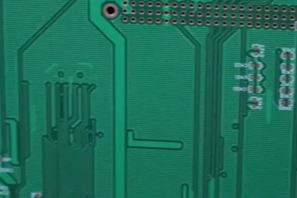
Having worked on high-frequency PCBs for years, I’ve come to understand that sometimes the most inconspicuous steps are the most prone to problems. For example, the seemingly simple drilling process actually hides many complexities.
I remember once we took on a radar module project where the boards used a special ceramic-filled substrate. The manufacturer we initially found assured us there wouldn’t be any problems, but the first batch of samples failed due to the hole wall quality. Later, when we disassembled them and looked under a microscope, wow, the hole walls were jagged like saw teeth, with micro-cracks barely visible to the naked eye, resulting in severe signal attenuation. This made me realize the importance of choosing the right high-frequency PCB manufacturer. Services really can’t be judged solely on appearances.
The properties of materials often determine the process route. For example, soft materials like PTFE and hard materials filled with ceramics have completely different requirements for drill bits. The former needs a sharper cutting edge to prevent wire drawing, while the latter requires drill bits with better wear resistance. The manufacturers we later partnered with would equip their machines with specialized drill bits for different materials, even changing parameters two or three times for mixed-material areas on the same board. This sounds troublesome, but it’s far more cost-effective than rework later.
Hole wall treatment is where a manufacturer’s expertise is truly tested. Some factories think simple cleaning before copper plating is enough, but the inert surface of high-frequency boards requires plasma or chemical activation to ensure copper layer adhesion. The boards we learned this the hard way… After the temperature difference test, the copper in the hole cracked open from the middle, separating layer by layer like peeling an onion. I later realized that factories that skipped the surface activation step simply couldn’t produce high-reliability products.
Now, when evaluating suppliers, I pay special attention to their ability to control details. For example, can they provide records of drilling parameter optimization for different materials? Do they have practical application cases of plasma treatment equipment? These seemingly trivial points are often more important than the brands on the equipment list. After all, even the most advanced machines need knowledgeable people to operate them.
In fact, high-frequency board manufacturing is like performing surgery; every step requires precise coordination. From material properties to drill bit selection to hole wall treatment, everything is interconnected. Sometimes, being slower is actually faster because the time wasted on rework is far greater than the time wasted on careful debugging.
When data centers upgrade their GPUs, the real bottleneck often hides in
When choosing a medical device PCB supplier, many overlook its decisive impact
Many people think that fast charging of electric vehicles only relies on
- Experte für die Produktion kleiner bis mittlerer Chargen
- Hochpräzise PCB-Fertigung und automatisierte Montage
- Zuverlässiger Partner für OEM/ODM-Elektronikprojekte
Geschäftszeiten: (Mo-Sa) von 9:00 bis 18:30