

What Documents Are Required for PCB Production: A Field Guide From Real Industrial Weighing Controller PCB Projects
Many engineers focus too much on technical parameters early on and overlook
I’ve always felt that the most interesting part of circuit board fabrication is that the unremarkable-looking details are often what decide success or failure. Take solder mask, for example — a lot of people assume it’s just a protective layer, but how it’s handled directly affects the reliability of the entire board, whether you’re building a simple two-layer board or a dense VoIP Phone PCB Assembly stack.
I remember once, a board we made had every design parameter meeting spec, yet it kept showing inexplicable short circuits during bench testing. It wasn’t until we opened it up that we discovered a certain area’s solder mask had slightly peeled under high-temperature conditions. This kind of problem is hard to catch during routine inspection and often doesn’t surface until actual use.
On silkscreen, I actually don’t think it’s necessary to chase excessive precision — though of course it depends on the specific application. For ordinary consumer electronics, slightly blurry characters don’t really affect usability, since pick-and-place machines these days all have vision-positioning systems anyway. But for medical or industrial equipment, clearer markings genuinely matter.
I’ve seen quite a few engineers push silkscreen line width below 0.1mm chasing extreme precision, only to end up with disastrous yield during mass production. In reality, as long as you stay above 0.15mm, most traditional processes can achieve it stably — why go looking for trouble?
Clients sometimes ask me why certain areas of solder mask are deliberately given 0.2mm more clearance than the pad. This is actually to accommodate the board material’s slight deformation under high temperature. That seemingly trivial fraction-of-a-millimeter difference can prevent a lot of potential problems in an environment with large temperature swings.
I recently tried a new circuit-board printing process and found it significantly improves solder-mask adhesion, especially in applications with frequent bending, where cracking becomes much less likely. That said, this process demands more from the silkscreen step — it needs a finer mesh count to guarantee character clarity.
At the end of the day, circuit board fabrication is more like an art of balance — you need to consider precision while also factoring in manufacturability. Blindly chasing a single parameter to the extreme easily traps you in a different pitfall elsewhere.
I’ve been in the circuit-board manufacturing business for quite a few years now, and I’ve seen plenty of factories talk endlessly about quality control while still tripping up on the details. Take circuit board printing, for example — many people assume that as long as the equipment is advanced, everything is settled.
Actually, what gives me the biggest headache is process parameters that swing up and down unpredictably. Walking the shop floor last week, I found the exposure machine’s temperature fluctuating like a roller coaster.
This kind of fluctuation shows up directly in the finished product — some boards have trace edges rough enough to scrape your hand.
We later introduced a metric called Cpk to quantify this kind of fluctuation.
Now, every time I see that number holding steady above 1.33 on a report, I genuinely feel reassured.
But staring at the number alone isn’t enough either. Once, a new engineer dialed the etching parameters to an extremely precise setting.
Guess what happened? The board’s impedance test failed across the board — the machine parameters were technically perfect.
So now I place much more weight on the interaction effect between parameters. It’s like cooking — you can’t just watch the heat; you also have to consider how the ingredients work together.
Laser direct imaging technology is trending in the industry lately, and it’s genuinely impressive, but I’ve noticed a lot of factories blindly jumping on the bandwagon.
Actually, an old-style exposure machine, as long as Cpk is kept stable, can still produce fine traces — what really matters is how skillfully a person operates the equipment.
I remember once helping a client handle a batch of boards with special substrate material, where conventional parameters simply didn’t apply.
We camped out on the shop floor for three days and three nights straight, and eventually found we had to apply reverse compensation between exposure energy and etch rate.
Cases like this make me feel that PCB manufacturing is really more of a craft — no matter how smart the machine, it still can’t replace a veteran technician’s experienced judgment.
Nowadays, some younger engineers rely too heavily on automated reports and, as a result, have lost their sensitivity to the process itself.
I often tell them: you need to touch the board edge with your hand, look at pad crystallization under a magnifying glass — these are the real quality signals that machine data simply can’t reveal.
I’ve always found the process of turning a circuit-board design into a physical object genuinely interesting. Many people assume it’s as simple as using a printer to copy a document — send over the design and get back an identical finished product. In reality, there’s far more nuance involved than you’d imagine.
I remember making this same mistake the first time I tried fabricating a circuit board myself. I spent several days drawing the routing diagram, sent it to the factory, and the finished product that came back was almost laughable. Traces that should have been perfectly straight came out crooked, and several critical pads had visibly shrunk in size. Worst of all, a tiny strand of copper had somehow connected two adjacent traces, scrapping the entire board outright. That experience taught me one thing: circuit board printing is nowhere near a simple image-copying process.
I later chatted with a veteran factory technician and learned that the entire fabrication process is more like a precise chemical reaction. The uniformity of the photoresist coating, the length of exposure time, the concentration control of the developer — every single step affects the final product’s precision. Sometimes even shop-floor temperature and humidity fluctuations create subtle differences in the outcome. This explains why the exact same design file can produce slightly different results across different production batches.
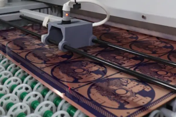
Now, when I look at the circuit-board printing process, I pay much more attention to the material’s own properties. Factors like the surface treatment of the copper-clad laminate and the sensitivity of the photosensitive material often matter more than the parameters in a design software. Sometimes, to achieve the desired precision, you need to reverse-adjust your design based on the specific production process. For example, in certain cases, appropriately widening trace spacing can actually produce a cleaner pattern edge.
Before submitting any design now, I always ask myself a few extra questions: is this trace width easy to keep intact under the current process? Has the spacing between adjacent components accounted for the possible error range? These considerations add to the upfront workload.
I’ve always found the most fascinating part of circuit board fabrication to be that seemingly insignificant details often decide success or failure. I remember once, working on a high-frequency board, running into a strange problem — the signal kept inexplicably attenuating. After a long struggle, we discovered the film had shifted slightly out of alignment during registration.
You might not imagine how much impact a millimeter-scale error can have. That time, our registration deviation was about 0.03mm — sounds insignificant, right? Yet that tiny deviation threw the entire impedance match completely off.
The step that tests patience most in circuit board printing is exposure. Many people assume setting the parameters is all it takes — it’s really not that simple. Factors like light angle and ambient temperature all affect the final result; sometimes the same batch of boards produces different results in the morning versus the afternoon.
I later developed a habit: before starting any new project, I always run a trial exposure at different exposure times first. This method takes more time, but it helps me find the setting best suited to current conditions, since every batch of material has slightly different characteristics.
Once, I ran into a particularly tricky situation where fine traces on a board kept coming out intermittent. At first, I assumed it was an etching problem and adjusted the solution concentration several times with no luck, only to later discover it was caused by uneven UV intensity during exposure, resulting in localized under-polymerization.
Now, when designing, I deliberately leave more room for adjustment rather than chasing extreme parameters, because I know unexpected situations will always crop up during actual fabrication — better to plan ahead than to fix things after the fact.
These experiences have taught me that circuit board fabrication is never a step-by-step, by-the-book process — it’s an art that requires responding to change at every turn, where every detail deserves careful attention.
I’ve recently been thinking about circuit board printing and realized a lot of people oversimplify it. Isn’t it just transferring a designed pattern onto a board? But anyone who has actually done it knows it’s not that easy. I remember the first time I tried printing a circuit board myself, full of anticipation, only to have the traces come out blurry, unable to guarantee even basic connectivity. That’s when I understood how many invisible hurdles stand between a pattern on screen and the actual finished product.
What’s most frustrating about circuit board printing is handling the details. You’d think a pattern drawn perfectly on a computer would transfer to the board exactly as-is? Reality often teaches you otherwise. For example, traces too thin are prone to breaking, while spacing too tight risks a short circuit. These seemingly minor differences can have a huge impact in actual application. Once, a board I designed had a pad-dimension deviation that prevented a component from soldering properly, forcing a complete rework.
Actually, print quality often comes down to the most fundamental steps. Choosing the right material matters a great deal — different board materials produce very different pattern-rendering results. Factors like ink adhesion and exposure time directly affect the final result. I later realized that instead of chasing fancy techniques, it’s better to first nail down the basics. Stable equipment, appropriate parameters, and careful operation matter more than any advanced trick.
Now, every time I see a circuit board I successfully printed, I think back to those failed attempts. It’s precisely those lessons that made me understand that circuit board printing isn’t a mechanically repetitive process — it’s a craft that requires constant adjustment and adaptation. Every project runs into new problems, and solving each one deepens my understanding of this technology. Maybe that’s exactly the appeal of fabrication — gradually mastering those seemingly simple but actually subtle techniques through repeated trial and error.
At the end of the day, accurately turning a design into a physical object is the biggest sense of accomplishment. When you see a circuit board’s pattern rendered clearly, with every trace connected correctly, that satisfaction is hard to put into words. This creative process of building something from nothing is perhaps what makes circuit board printing so compelling.
I’ve seen too many people oversimplify circuit board fabrication — especially newer engineers, who often assume that once the design drawing is sent to the factory, the job is done.
In reality, the most exhausting steps often show up in the most unremarkable places.
Take circuit board printing, for example — many people assume that as long as the trace design is correct, everything’s secure, overlooking just how much post-processing affects the finished product, whether it’s a small run of double-sided boards or a full VoIP Phone PCB Assembly build headed for volume production.
I remember once our team was rushing to deliver a batch of high-density boards, and sample inspection before shipping found the traces near the edge were noticeably thinner than those in the center.
At first, everyone assumed it was a deviation from the design software’s export process. After repeatedly double-checking the files with no issue found, we eventually discovered the real problem was in the etching stage.
Etching solution flows faster along the board’s edge, causing excessive corrosion of the copper foil, while liquid retention in the center area meant insufficient corrosion there — a detail that nearly delayed the entire project.
We later adjusted the fixture design to keep the board tilted at a specific angle inside the etching tank. It added an extra operational step, but it effectively improved uniformity.
Speaking of solder mask, this really is a step that demands patience — especially when handling fine-pitch components, where that thin solder-mask layer becomes practically an art-level operation.
I’ve seen people, to save effort, thin out the solder-mask ink too much, only to have it flow and deform during the drying stage — leaving areas that should be covered exposed, while areas that shouldn’t connect end up stuck together.
The most troublesome designs are the ones requiring a fine solder-mask dam — with a gap under 0.1mm, even a slight deviation can cause adjacent pads to short during reflow soldering.
Once, during acceptance, we found solder bridging under a BGA chip. Rework required using a microscope to scrape away the excess solder paste bit by bit — a process that was a real test of both eyesight and hand steadiness.
Now, whenever I encounter this kind of fine work, I require the factory to run a process validation with a test board first, specifically checking solder-mask-dam integrity — after all, the cost of later repair far exceeds the cost of upfront prevention.
Honestly, spending enough years in this business, you realize what genuinely determines final quality often isn’t some sophisticated design software — it’s these seemingly basic process details.
Every step is worth investing time into refining, because nobody wants to see their carefully designed board turn into scrap because of a fabrication-process issue, right?
I’ve seen too many beginners make the same mistake when designing circuit board printing — they always think making markings as prominent as possible is better. Once, checking a friend’s design draft, I found he’d placed a component’s number directly on top of a pad — that white number, printed on shiny copper foil, was almost invisible. Later, when the factory opened the solder-mask window, those characters got cut in half.
Actually, the relationship between silkscreen and pads is a bit like road markings on a street — you wouldn’t paint a parking space over a crosswalk, would you? Keeping appropriate distance actually makes both elements clearly visible. I’ve made it a habit to leave silkscreen some breathing room — even shifting it just 0.1mm makes a big difference.
Color pairing is a whole discipline of its own. Last year, I saw a board using dark green solder mask paired with grayish-blue silkscreen — workers on the assembly line had to lean in close just to read the markings, directly slowing down assembly efficiency. Switching back to white text on a green background immediately made things much smoother. This kind of contrast choice really isn’t something you decide by feel.
On copper-foil handling, many people only focus on conductivity performance while overlooking surface condition. Once, I tested a substrate with excessive surface roughness, and after etching, the trace edges came out jagged like a saw blade — thankfully, switching to smoother copper foil in time preserved the precision circuit’s integrity. This made me realize that every step, from copper foil to final formation, is interconnected and mutually constraining.
Oxidation is the most easily overlooked issue. Once, disassembling a board that came back for repair, I found a trace break was actually caused by an oxide layer causing dry-film adhesion failure. Now, before submitting any board for production, I always confirm the material storage conditions — after all, nobody wants an invisible flaw to ruin an entire batch of boards.
A genuinely reliable design tends to show up precisely in these details — it’s not about piling on technical parameters, but about making sure every element plays its proper role. Sometimes simplifying the layout actually works better than complex adjustments.
Every time I look at the fine traces on a precision circuit board, I think back to the pitfalls I ran into when I first got into circuit board printing. Many people assume that once the design drawing goes to the factory, the job’s done — in reality, there are far more overlooked details hiding between drawing and finished product than you’d expect.
I remember once designing a high-frequency circuit, deliberately controlling the trace width to a very fine dimension. The sample came back and the signal was completely off — after a long investigation, we found an unexpected deviation had occurred during the etching process. That’s when I truly understood that circuit board printing isn’t a simple copy-paste process — it’s an art that requires comprehensively weighing material properties against process limitations.
The etching stage is especially easy to trip up on. When the chemical solution corrodes away the excess copper layer, it doesn’t just act straight down — it also erodes sideways along the trace edges. This phenomenon is known in the industry as the side-etch effect, and it causes the actual formed trace to come out considerably thinner than the design value. For example, if you design a 5-mil trace width, after accounting for the etching factor, the effective conductive width remaining might only be around 3 mils.
Now I’d recommend beginners leave more margin in their designs. Rather than chasing theoretical extreme precision, it’s better to focus on making the design more adaptable to actual production conditions. Sometimes, adding just a few extra mils to trace width can avoid the risk of scrapping an entire batch. After all, a circuit board is meant to be used — it’s not an art piece meant for admiration under a microscope.
A genuinely reliable manufacturer won’t just boast endlessly about how high their processing precision is — they’ll honestly tell you which designs are prone to problems in actual production. That kind of experience is often more valuable than the numbers on an equipment spec sheet.
Recently, while checking a friend’s power-board design, I found he’d made certain traces too thin in pursuit of a compact layout. Even though the calculations looked fine in theory, factoring in process variation during mass production, I still suggested widening the critical traces. He later told me that batch’s yield was exceptionally high — which further convinced me that a bit of conservatism in circuit board design isn’t a bad thing.
At the end of the day, good circuit board design should strike a balance between the ideal and reality. You shouldn’t over-design out of fear of risk, nor should you ignore the objective realities of the manufacturing process in pursuit of the extreme. Getting that balance right usually takes a few failures to truly master.
I’ve always found circuit board printing a genuinely interesting subject. A lot of people always want to make traces as fine as possible, overlooking the fluctuation margin inherent in actual production. I remember once, my design had trace spacing pushed right to the limit, and the factory’s finished yield was especially low. I later realized that leaving some room for production actually turns out to be more reliable.
Take the concept of design margin, for example — it’s not just adding a simple percentage to your design values. You have to factor in material properties, equipment precision, and even seasonal shifts in shop-floor environment. Once, a board made in summer developed a micro-short in winter simply because humidity changes caused different solder-mask shrinkage rates. Now I’ve made it a habit to leave 20% extra spacing around critical signal lines — it slightly increases board area, but it earns stable yield in return.
What circuit board printing fears most is assuming things without verifying. I’ve seen quite a few engineers treat simulation results as the final plan, only to run into all kinds of problems during mass production. In reality, simulation models are always idealized, and tolerance accumulation on an actual production line often exceeds expectations. The most practical lesson in this business is: don’t chase the theoretical optimum — find the practical, workable solution instead.
One supplier I’ve worked with handles this quite cleverly. Instead of promising maximum precision no matter what, they recommend an appropriate process grade based on your design’s complexity. Once, I insisted on using the smallest possible trace width, and they directly showed me a stack of defect photos — designs that looked flawless on paper, riddled with broken traces and shorts once they hit the real world.
Now, when I design, I deliberately set parameters at the middle of the process window rather than pushing against the lower limit. For example, if a factory says they can achieve a 4-mil trace width, I’ll design for at least 4.8 mil. This seemingly conservative approach has actually sped up project timelines, because it eliminates the need for repeated sample iterations.
A recent project made me even more convinced of this. The client wanted complex routing on a high-density board, and the initial plan nearly maxed out every process limit. We later redesigned the layout, adding 20% design margin to critical areas — the overall dimensions grew somewhat, but it passed reliability testing on the very first trial run.
Actually, good circuit-board design is a lot like cooking rice — too much heat scorches the pot, while leaving room for steam to escape produces fragrant, well-cooked rice. Designs that try to use every single square millimeter to its absolute limit often end up spending far more later fixing mass-production problems.
Sometimes, letting go of the obsession with extreme parameters actually produces more stable product performance. This is probably the difference between engineering thinking and academic thinking — what we ultimately want is a physical object that can be mass-produced, not a perfect plan that stays on paper.
I’ve always felt Leiterplattenfertigung gets over-mystified. Every time I see an article discussing precision manufacturing, I can’t help but smile — they always attribute the issue to equipment precision or material selection.
In reality, what actually affects circuit board quality is often the unremarkable, day-to-day detail. For example, temperature fluctuation in the workspace alone can undo an entire printing process. I remember once, running an experiment in my own garage, I noticed something interesting: the same-spec copper-foil substrate produced clearly different results depending on where it was placed — the board closer to the window came out with noticeably rougher trace edges after etching.
Many people obsess over pushing trace width extremely thin, overlooking a basic fact: once a trace gets thin enough, current-transmission efficiency actually drops. I ran a comparison test — widening an originally designed 3-mil trace to 5 mils actually made signal integrity more stable, likely because a wider conductor provides a more stable electromagnetic environment.
On circuit board printing technique, I think there’s a common misconception today — overemphasizing equipment sophistication while underestimating operational experience. Once, visiting a friend’s lab, I saw a laser direct-imaging system they’d spent a fortune on, but because the operator wasn’t familiar with temperature-and-humidity control, the final yield actually came in lower than what a veteran technician achieved using a traditional exposure machine.
On the etching process, I found something interesting — a lot of tutorials suggest extending etch time to improve precision, but in reality, over-etching actually causes jagged burring along the trace edge. I later tried switching from conventional immersion etching to spray etching, and not only did it cut process time by a quarter, but side-etch amount also dropped by 30%.
What surprised me most was the substrate pretreatment step. Once, on a whim, I placed copper foil in a constant-temperature chamber for 24 hours before pattern transfer, and found that even with the most ordinary wet-film process, we could achieve a 2-mil trace width close to dry-film precision — suggesting that internal stress balance in the material might matter more than we assume.
Fabricating a circuit board is really a lot like cooking a dish — too much heat and it burns, too little and it stays undercooked. The key is finding exactly the right balance point. Sometimes, deliberately chasing a single parameter actually disrupts the harmony of the entire system.
Many engineers focus too much on technical parameters early on and overlook
As someone who has worked in PCB outsourcing for years, I’ve found
Cramming a camera, amplifier, dual-mic array, and Wi-Fi radio into a palm-sized
- Experte für die Produktion kleiner bis mittlerer Chargen
- Hochpräzise PCB-Fertigung und automatisierte Montage
- Zuverlässiger Partner für OEM/ODM-Elektronikprojekte
Geschäftszeiten: (Mo-Sa) von 9:00 bis 18:30
Get quote, solution or any question, Andre always here to help