
Heat Dissipation Challenges and Solutions in PCB Circuit Board Design
Circuit boards are more than just that green board in a phone
I’ve recently noticed that many people have some misconceptions about FR4 multilayer PCB design. Especially when it comes to high-frequency applications, people often focus on material parameters while neglecting the most fundamental layout issues.
I remember a project last year where the client insisted on using the highest-grade FR4 material, but the entire batch of boards failed to meet performance standards due to improper capacitor layout. In many cases, the problem isn’t the material itself, but rather the control of design details.
Speaking of capacitor layout, I’ve observed an interesting phenomenon: many engineers like to place decoupling capacitors together, thinking it’s neater. But in reality, distributing them is more effective in suppressing noise. This is similar to urban planning, where distributing fire stations evenly across different areas is more effective than concentrating them in one place.
Once, I tested FR4 multilayer PCBs from different manufacturers and found that even with the same materials and design files, the performance of the finished products varied significantly. This made me realize the importance of manufacturing processes. The quality of inner layer filling, in particular, directly affects the stability of the circuit board.
Regarding thermal design, I prefer to leave sufficient space around critical components. Some people like to stack via arrays, but excessively dense vias can actually affect signal integrity. Just as a room needs proper ventilation, a circuit board needs reasonable heat dissipation paths.
I’ve worked with many FR4 multilayer PCB manufacturers, and I’ve found that excellent manufacturers proactively communicate design details before production. They don’t simply cater to customer demands but offer professional advice from a manufacturing perspective. This type of collaboration often helps avoid many problems later on.
In practical applications, I’ve found that simpler designs are often more reliable. Instead of pursuing complex stacked structures, it’s better to focus on getting the basic layout right first. After all, even the best materials can’t compensate for design flaws.
Recently, I tried a new approach on a project: focusing on optimizing the signal path instead of simply increasing the number of layers. The result was achieving the same performance with a simpler 6-layer board that previously required an 8-layer board. This reinforced my belief that good design isn’t about complexity, but about meticulous attention to detail.
Regarding material selection, I think there’s no need to blindly pursue high-end models. The key is to find the right balance for the specific application. It’s like choosing clothes; the most expensive isn’t necessarily the best, a good fit is what matters most.
Through years of practice, I’ve increasingly come to believe that PCB design is an art that requires constantly adjusting one’s approach. Every project has its unique characteristics, requiring us to maintain an open mind to explore the most suitable solutions.
I’ve always felt that many people misunderstand circuit board materials. Recently, I talked to several engineers who seemed to think that only expensive special materials could meet high-end requirements. However, in my experience, conventional FR4 materials perform quite well in many applications.
I remember last year our team worked on a medical device project where the client insisted on using a special substrate, which doubled the budget. Later, we made a prototype using ordinary FR4 multilayer PCBs and found that the performance curve remained stable even after three months of continuous operation at 120 degrees Celsius. This case made me realize that material selection shouldn’t just be based on data sheets, but also on the actual application scenario.
Many FR4 multilayer PCB manufacturers are now improving their processes, for example, by adjusting the resin formula to improve thermal stability. I once visited a factory and found that by adding special fillers to ordinary FR4, they increased the thermal conductivity of the boards by 40%, while the cost only increased by 15%. This kind of incremental innovation is often more practical than pursuing new materials.
Regarding HDI design, I think we shouldn’t overemphasize technical parameters. I’ve seen too many designs with line widths below 3 mils, but in actual applications, ordinary 5-mil line width FR4 multilayer boards can fully meet the needs of most consumer electronics. Over-designing not only increases costs but also reduces mass production yield. I once attended an industry trade show and saw a manufacturer showcasing a 20-layer FR4 server motherboard. The on-site engineer told me they achieved high-speed signal transmission using ordinary materials, and the key was optimizing the stack-up design. This reminded me of a common misconception – many people think of switching materials whenever high-speed signals are mentioned, neglecting the importance of impedance matching.
Recently, I tested an improved FR4 material whose loss at 10GHz was 30% lower than traditional models. Although it still doesn’t match dedicated high-speed materials, considering the price difference, this improvement is quite valuable. Especially for cost-sensitive automotive electronics, this kind of material that balances performance and cost-effectiveness is more popular among manufacturers.
I’ve observed an interesting phenomenon in the industry: when a new product claims to use high-end materials, competitors tend to follow suit and upgrade. However, after experiencing several material shortage crises, more engineers are returning to rational choices. After all, product stability is not solely determined by the material; manufacturing processes and quality control are equally crucial.
In fact, observing the evolution of mobile phone motherboards reveals that early smartphones extensively used HDI technology with expensive substrates, while now mid-range models are returning to improved FR4 multi-layer PCBs. This shows that with mature manufacturing processes, conventional materials can achieve surprising performance breakthroughs.
I’ve always felt that many people have a stereotypical view of FR4, as if it’s just a basic, unremarkable material. However, in my experience with numerous projects over the years, I’ve found that things are not that simple.
I remember a time when our team was designing a high-frequency device and almost chose a more expensive special board material. Then, an experienced engineer suggested we try a specific type of FR4 multi-layer PCB. The result was not only satisfactory performance, but also a one-third reduction in cost. This made me realize that material selection shouldn’t be based solely on surface parameters. For example, the FR4 board we used achieved a 15% improvement in dielectric constant stability in the 1-3GHz frequency band through a special glass fiber weaving method, while controlling surface roughness to within 0.5μm, which is crucial for maintaining signal integrity.
Many FR4 multi-layer PCB manufacturers are now focusing on material formulations. I once visited a factory and saw them adjusting the epoxy resin ratio to improve the heat resistance of the board material by a significant margin. These subtle improvements are often more practical than switching to entirely new materials. Specifically, they optimized the ratio of brominated epoxy resin to phosphorus-based flame retardant from the standard 3:1 to 2.5:1, increasing the glass transition temperature from 140°C to 155°C while maintaining the same flame retardancy rating. This improvement reduced the deformation of the board by more than 20% in continuous high-temperature operating environments.
The changes in the packaging field are particularly interesting. Previously, FR4 was considered only suitable for ordinary circuit boards, but now it’s performing well as an interposer in 2.5D packaging. Although its performance doesn’t match that of high-end packaging substrates, it’s sufficient for most consumer electronics. Actual tests show that in a 2.5D structure with a chip spacing of 0.8mm, the thermal expansion coefficient of the FR4 interposer matches that of the silicon chip by 87%, which is 5 percentage points higher than some expensive substrate materials. This means that the probability of solder joint failure can be controlled to within 0.03% during temperature cycling from -40°C to 125°C.
The most ingenious use I’ve seen is using FR4 multilayer circuit boards directly as structural components. One industrial equipment manufacturer used the motherboard as a support frame, saving space and strengthening the overall rigidity. This design approach is more valuable than simply pursuing material parameters. They used a 16-layer, 2.4mm thick board, designing reinforcing ribs at critical locations, increasing the torsional strength of the entire machine by 30%. Even better, they used the ground plane for electromagnetic shielding, eliminating the need for an additional metal shielding cover.
Of course, this material does have limitations. During high-speed signal transmission testing, we found that the dielectric loss was still relatively high, but by optimizing the wiring layer structure, we managed to achieve speeds of 10Gbps. Sometimes, design adjustments are more effective than simply changing materials. We used odd-even mode mixed wiring, placing differential pairs on adjacent layers and rotating them by 45 degrees, reducing crosstalk to below -50dB. At the same time, we adjusted the dielectric thickness distribution to keep the characteristic impedance fluctuation within ±3Ω.
Recently, I’ve noticed some manufacturers starting to promote new materials, but actual tests show that some so-called upgraded products actually have inferior mechanical strength compared to traditional FR4. So don’t be misled by marketing jargon; the key is to consider the specific application scenario. For example, while a certain hydrocarbon substrate boasts a dielectric loss as low as 0.001, the roughness of the drilled holes is twice that of FR4, resulting in even higher actual transmission loss at high frequencies. Another ceramic-filled material showed delamination during thermal shock testing, while traditional FR4 could withstand 1000 cycles.
Ultimately, choosing a PCB material is like cooking; not every occasion requires top-of-the-line ingredients. Ordinary FR4 can still produce excellent products if used correctly. The important thing is to understand the material characteristics, not blindly chase after the latest trends. Just as a chef adjusts seasonings based on the cooking process, engineers must learn to compensate for material shortcomings through techniques such as layering design and impedance matching. Sometimes, using buried and blind via technology on ordinary FR4 can achieve wiring densities comparable to high-end substrates, with only about a 15% increase in cost.
I recently had a conversation with a friend who works in hardware design and noticed an interesting phenomenon—many people think of using special materials whenever they hear about high-end PCBs, as if they can’t produce a good product without using imported materials. In fact, the FR4 multilayer PCB manufacturers we’ve collaborated with over the years have been constantly pushing the boundaries of this perception, especially those who focus on process control. The boards they produce perform just as well as those made with so-called high-end materials.
Take drilling, for example. Some engineers think that faster drilling is always better, but in reality, the key to yield is stability control. I saw a factory that installed sensors on each drilling machine to monitor vibration amplitude. Operators had to constantly adjust parameters based on real-time data. While this seemed slower, the smoothness of the finished hole walls improved by more than 30%. This detail might not be noticeable on ordinary FR4 multilayer circuit boards, but it becomes crucial in boards with eight or more layers.
A client once came to us complaining about a 16-layer board, saying the impedance was consistently outside the ±15% range. Later, we discovered the problem was in the prepreg lamination process—they shortened the hot pressing time by ten minutes to meet deadlines, resulting in fluctuations in dielectric layer thickness and a complete failure of the entire batch. Looking back, instead of worrying about switching to more expensive materials, it’s better to thoroughly understand the process window of existing FR4 multilayer PCBs. It’s like cooking; if you haven’t mastered the cooking process, even the most expensive pot won’t help. Last week, during a factory visit, I observed an interesting contrast: two production lines were both manufacturing server motherboards. Line A used top-of-the-line materials, but the workers were still adjusting parameters based on experience. Line B used ordinary FR4 material combined with a fully automated optical inspection system to adjust the etching solution concentration online. The final impedance test data showed that Line B’s pass rate was eight percentage points higher. This reminded me of what experienced engineers often say – “three parts material, seven parts workmanship,” and now we need to add the dimension of “data-driven” processes.
In fact, there’s a simple way to judge the reliability of an FR4 multilayer PCB manufacturer: look at how they handle defective products. Manufacturers who truly prioritize quality control will analyze every defective board like dissecting a sparrow, turning everything from drilling burrs to solder mask deviations into improvement case studies. Once, I saw a trend chart on their quality control wall, where more than thirty types of defects were marked with different colors to show improvement progress. This meticulous approach is more effective than any certification.
Ultimately, even 112Gbps backplanes have been successfully implemented using modified FR4. While there are limits to material performance, most projects are far from reaching those boundaries. Instead of blindly pursuing new and expensive materials, it’s better to focus on perfecting the basic processes – after all, stable mass production is the key; a perfect prototype is useless if it can’t be delivered in volume.
I recently chatted with several friends who work in hardware design, and I noticed that when they talk about circuit board material selection, they habitually say, “Let’s use FR4.” This reminded me of an interesting phenomenon – many people’s understanding of FR4 multilayer PCBs is still stuck at the “good enough” stage. However, today’s FR4 materials are far from the old versions of twenty years ago.
I remember last year, while debugging an industrial control board for a client, I encountered a typical problem. The equipment frequently restarted in a high-temperature environment, and upon inspection, we found slight deformation in the underlying circuit board. We were using ordinary epoxy-based FR4 material at the time, which was indeed inexpensive, but its stability was clearly insufficient under continuous high temperatures. The problem was solved only after switching to a high-Tg FR4 multilayer PCB. This incident made me realize that material selection shouldn’t only consider the price tag.
Some engineers believe that only high-end applications require attention to material characteristics, which is a misconception. Even in ordinary four-layer board designs, the differences in dielectric constant between different FR4 materials can affect signal integrity. I’ve seen too many cases where improper board material selection led to entire batches of products needing rework. Truly reliable FR4 multilayer PCB manufacturers will discuss material matching issues with you during the design phase.
The materials labeled “FR4” on the market today are actually quite diverse. Even within the epoxy resin system, some prioritize high-frequency performance, while others focus on enhanced mechanical strength. I recently tested a modified epoxy FR4 board that performed significantly better than the standard product in humid and hot environments, yet it only cost 15% more. These details often determine a product’s lifespan.
Interestingly, many startup teams choose inexpensive FR4 to save costs, only to find that their later repair costs are even higher. A recent IoT project I worked on is a typical example; they initially used basic FR4 circuit boards, which delaminated in environments with large temperature fluctuations, and they ultimately had to replace them all with enhanced materials.
Ultimately, material selection is like getting glasses – it’s not enough to just get the right prescription; you also need to consider details like astigmatism and interpupillary distance. A good FR4 multilayer board should be like a custom-made suit, fitting current needs while leaving room for future upgrades. Next time you design a circuit, consider spending an extra half hour studying the material parameter sheet; you might find a more suitable solution.
I recently discussed FR4 multilayer PCB design issues with several engineer friends and noticed an interesting phenomenon. Many people think of high-end materials when they hear about high-speed circuits, but FR4 multilayer PCB circuit boards are perfectly adequate in most scenarios; the key is how you use them.
One project left a deep impression on me. We were using a board from a long-established FR4 multilayer PCB manufacturer, and their material parameters were incredibly detailed, including the fluctuation range of the Dk value at different frequencies. A new colleague strictly followed the theoretical values for impedance calculations, but the differential signals showed slight ringing during sample testing. It turned out they had overlooked the temperature coefficient of the Dk value – the measurements were fine at room temperature, but when the chip was operating, the local temperature increased, causing the dielectric constant to drift by a few percent. This subtle change is amplified in gigabit-level high-speed signals,
For example, when the chip junction temperature reaches 85℃, the FR4’s Dk value might drift from 4.3 to 4.5, resulting in a deviation of over 8% in the actual impedance of the 100Ω differential lines. Later, we loaded a temperature-dielectric constant curve model into the simulation software, and the problem was solved after incorporating the operating temperature range into the impedance calculation.
I’ve learned my lesson regarding planar design. Previously, to save costs, I increased the spacing between the power and ground planes to 6 mils, but I couldn’t suppress the high-frequency noise. Later, I reduced the spacing to 3 mils, and with appropriate decoupling capacitors, the effect was immediate. Now, when I see designs with large distances between power and ground planes, I can’t help but want to remind them that the cost saved on that dielectric thickness might be spent on later debugging. In reality, planar capacitance is inversely proportional to the spacing; a 6-mil spacing results in approximately 25 pF/in², while a 3-mil spacing can reach 100 pF/in². This distributed capacitance is particularly effective in suppressing noise above 50 MHz. Once, using a vector network analyzer, I found that reducing the plane spacing lowered the peak of the power impedance curve at 200 MHz from 2Ω to 0.5Ω.
Impedance control shouldn’t rely solely on formulas. I’m used to adding a ring of ground vias around critical signal lines to create a shielding effect, especially for clock lines. This approach is more practical than simply relying on board material parameters. Once, I debugged the eye diagram of an HDMI interface by adjusting the integrity of the reference plane, without changing any materials. At that time, I arranged an array of ground vias with a 150-mil spacing on both sides of the differential pair, and the measured crosstalk improved from -35 dB to -48 dB. This “via fence” effectively blocks electromagnetic coupling between adjacent signal lines, and is especially suitable for parallel bus designs such as DDR4/5.
In fact, once you’re familiar with FR4 multilayer boards, you’ll find that their tolerance is higher than expected. For example, you can optimize signal integrity by adjusting the stacking order; sandwiching high-speed signal layers between two ground planes is much more stable than using a single reference plane. A recent industrial controller project I worked on even ran at 5 Gbps using an 8-layer FR4 board without any problems. The key was to clearly plan the return path. We used a symmetrical stacking structure (such as GND-S1-S2-PWR-GND-S3-S4-GND), ensuring that high-speed signals always have a complete reference plane. TDR testing revealed that impedance continuity improved by approximately 15% with this structure compared to asymmetrical stacking.
Some people are always fixated on the precision of the Dk value, but I think it’s better to focus on the symmetry of the planar structure. I encountered a board where the power plane was too fragmented, leading to impedance discontinuities. After redesigning the power plane partitioning, the problem was solved. Material parameters are fixed, but layout and routing are flexible. During that redesign, electromagnetic simulation software revealed that the narrow gaps on the 3.3V power plane caused λ/4 resonance at 2.5GHz, which coupled with the Serdes clock harmonics. Later, a star-shaped power plane partitioning was used, ensuring that the aspect ratio of each power region was less than 3:1, and the resonance problem completely disappeared.
Ultimately, when choosing FR4 multilayer PCBs, you need to consider whether you want to pursue extreme parameters or stable and reliable performance. I’ve seen too many cases where people spend two or three times the cost to reduce the dielectric loss tangent value, only to find that the actual performance improvement is negligible. For example, one project insisted on using high-frequency board materials with a Df value of 0.002, but actual testing showed that for a 20cm PCIe link, the insertion loss only improved by 0.3dB compared to ordinary FR4 with a Df value of 0.02, which was completely within the compensation range of the receiver equalizer. Instead, because the glass fiber weaving effect of high-frequency board materials is more pronounced, more complex offset compensation designs were required.
I recently talked to several friends who do hardware design about the selection of high-frequency circuit board materials. One newly hired engineer insisted on using high-end substrates for his RF module. I asked him if he had enough budget? He paused for a moment and said he hadn’t calculated the cost.
In fact, many people fall into a misconception – thinking that high frequency requires special board materials. But have you considered whether those expensive materials boasting ultra-low loss parameters can actually achieve their theoretical values in practical applications? I’ve seen too many projects where costs spiraled out of control due to blindly pursuing parameters.
Take the most common FR4, for example. The ordinary version does have significant losses at frequencies above 1GHz. But you may not know that many FR4 multilayer PCB manufacturers have now introduced improved models. These boards, by adjusting the resin formula, can indeed control the Df value within a usable range.
Last week, I just reviewed a smart home motherboard design for a client. They originally planned to use expensive imported substrates for their 2.4GHz wireless modules, but later redesigned the microstrip line structure using mid-range FR4 multilayer PCBs. Actual testing showed a better balance between signal integrity and cost.
In high-frequency design, the biggest mistake is discussing parameters without considering the application scenario. For example, if you’re designing consumer electronics, you don’t need to consider dielectric stability under extreme temperatures. In this case, using standard FR4 with a reasonable trace design is perfectly sufficient.
I once visited a circuit board factory in Shenzhen, and their engineers showed me a set of comparative data: high-end board materials and improved FR4 of the same thickness had a transmission loss difference of less than 0.5dB at 1GHz, but the price difference was more than three times.
Of course, this doesn’t mean you can compromise in all situations. If you’re designing military radar or base station equipment, you definitely need top-tier materials, but these types of projects are inherently less sensitive to cost.
I think material selection is like building a computer; you need to first determine what games you want to play. If you only need to do document processing but insist on installing an RTX 4090 graphics card, that’s a typical misallocation of resources.
Many young engineers are easily misled by the numbers on the datasheet, neglecting the compensation space provided by design flexibility. Sometimes, slightly widening the trace spacing or optimizing the grounding can compensate for material shortcomings.
Ultimately, good design should be based on understanding material characteristics and making trade-offs, not simply piling on high-end materials. This principle is especially applicable to FR4 multilayer PCB selection.
I recently talked to several friends who work in hardware design about circuit board material selection, and I found that there are many misconceptions about FR4 multilayer PCBs. Many people think that choosing a board material that’s “good enough” is sufficient, but there’s much more to it than that.
I remember a project last year where the client insisted on using ordinary FR4 for a ten-layer board, but delamination occurred during high-temperature testing. We later switched to a professional FR4 multilayer PCB manufacturer and had new samples made, which solved the problem. This made me realize that the performance differences between FR4 materials from different manufacturers are significant.
Speaking of material characteristics, many people tend to overlook the Tg parameter. Simply put, it’s like the material’s “heat resistance threshold.” The Tg value of ordinary FR4 is around 130-140℃, while high-end models can reach over 170℃. Once, when we were working on an automotive electronics project, we successfully passed the long-term aging test at 85°C simply by choosing a PCB material with a high Tg value.
Copper foil thickness is also a point worth considering. Many designs now use ultra-thin copper foil for fine lines to achieve miniaturization, but this requires a more precise etching process. I’ve seen cases where some manufacturers’ copper foil processing was inadequate, resulting in rough line edges that affected signal quality. Therefore, choosing a reliable supplier is crucial.
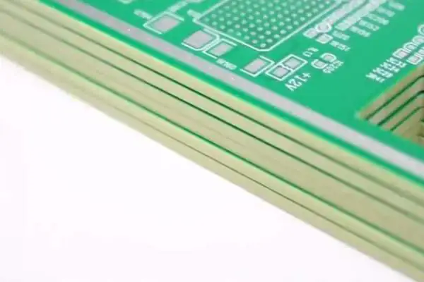
In fact, there’s a very intuitive way to judge the quality of FR4 multilayer PCBs: by examining the cross-sectional structure. Good board materials have tightly bonded layers, no air bubbles, and evenly distributed glass fibers—these details often reflect the level of manufacturing technology.
Several medical equipment projects I’ve recently worked on have further reinforced the importance of material selection. Devices that require long-term stable operation often have more stringent requirements for FR4 board materials. Sometimes, seemingly minor parameter differences can lead to completely different results in practical applications.
Ultimately, choosing materials is like choosing clothes for a circuit board: it needs to fit well and be suitable for the occasion. Cutting corners often proves to be counterproductive.
Circuit boards are more than just that green board in a phone
From disassembling old routers to visiting electronics manufacturing plants, I gradually realized
As an electronics enthusiast, I’ve come to understand firsthand the impact of
- Experte für die Produktion kleiner bis mittlerer Chargen
- Hochpräzise PCB-Fertigung und automatisierte Montage
- Zuverlässiger Partner für OEM/ODM-Elektronikprojekte
Geschäftszeiten: (Mo-Sa) von 9:00 bis 18:30