
Why is the material selection of the RF Front End PCB crucial?
The performance bottleneck of an RF front end is rarely the chip
While recently organizing my home networking gear, I stumbled upon several old 2-port PCB switches. These little devices may look simple, but they quietly play a vital role in a wide variety of scenarios. Many people might assume that such compact switches offer limited functionality; however, their flexibility and adaptability are, in reality, frequently underestimated.
I recall helping a friend revamp the network layout in an old house; the cabling throughout the entire building was quite complex. Initially, we considered using a large-scale switch for centralized management, but we had to account for the issue of signal attenuation across different floors. Ultimately, we decided to place one of these compact PCB switches at key nodes on every floor. The results were unexpectedly impressive; the signal stability proved to be far superior to what we had anticipated.
The PCB design of these switches is actually quite sophisticated. Although they feature only two ports, the internal circuit layout directly influences data transmission efficiency. I have disassembled and examined similar products from several different brands, and I discovered that those models which consistently operate stably over the long term tend to excel in terms of circuit board heat dissipation and interference shielding. Sometimes, a simpler design actually proves to be the more reliable choice.
Nowadays, many smart home systems are beginning to adopt a similar philosophy. Rather than striving for a single point of central control, they opt to deploy small network nodes across various zones. This distributed architecture not only mitigates the risk of a “single point of failure” but also enhances the overall resilience of the network. I personally use a modified 2-port switch in my home study to connect my computer and NAS; it has been running flawlessly for over three years without a single issue.
Of course, these devices do have their limitations—the limited number of ports is indeed a significant drawback. However, for specific scenarios, this seemingly restrictive configuration actually becomes an advantage—much like building with LEGO blocks, where a robust network structure is constructed by combining multiple small, modular units. They are often more flexible and controllable than a single, large-scale device.
Recently, I’ve noticed some DIY enthusiasts starting to experiment with designing their own network switch PCBs. Although the resulting prototypes are still quite rough around the edges, this spirit of exploration is fascinating. After all, only by understanding the underlying principles can one truly unlock a device’s full potential.
Ultimately, the choice of network equipment is never a black-and-white issue. The key lies in finding a solution that precisely meets your actual needs. Sometimes, the most unassuming, basic configurations are the ones that best stand the test of time.
I’ve personally undertaken numerous minor modifications to network devices, and I’ve found that the humble 2-port PCB network switch is a particularly interesting piece of kit. Many people assume that switches are only necessary for large-scale networks, but this is simply not the case.
In my studio, I prefer to manage different types of equipment in separate segments—for instance, assigning photography gear to one network subnet and 3D printers to another. In such scenarios, a simple dual-port switch makes it effortless to achieve this isolation; it requires no complex configuration—you simply plug it in and it works. This is especially true for those compact boards featuring dedicated chips; they are small, consume very little power, and can be tucked away and secured in just about any corner.
On one occasion, while modifying an old router, I discovered that its internal switch chip was running at a shockingly high temperature. After replacing it with an industrial-grade chip equipped with a heatsink, the situation improved dramatically. In reality, the choice of chip directly impacts a device’s stability. Some budget-oriented solutions cut costs by utilizing salvaged components—parts stripped from other devices—which often leads to premature failure.
Nowadays, I tend to gravitate toward products that clearly specify the model of the chip being used. At the very least, knowing exactly which manufacturer’s solution is inside gives me peace of mind. For instance, some manufacturers might pass off consumer-grade chips as industrial-grade ones—a subtle detail that the average user would never be able to spot.
Another advantage of dual-port switches is their flexibility. You don’t have to buy a bulky 8-port switch just to connect two devices—a move that would merely take up space and waste resources. For example, I have a small switch connected directly between my desktop PC and my NAS; as a result, file transfer speeds are noticeably faster than they would be if the data had to pass through my main router.
When setting up your cabling, it’s crucial to pay attention to the quality of the PCB itself. I once tried to save a few bucks by buying a cheap board, only to find it had poor contact at the ports and frequent disconnections; I later discovered that the gold plating on the contacts was simply too thin. High-quality boards feature significantly thicker “gold fingers” (the contact pads), ensuring a secure connection that remains stable even after repeated plugging and unplugging.
Ultimately, the greatest vulnerability of these small devices is instability. After all, if a network connection goes down, troubleshooting the issue can be an incredibly tedious and frustrating process. Consequently, I now make it a rule to test any new device by letting it run continuously for a full week; I won’t put it into active service until I’ve confirmed that it operates without any issues.
While recently debugging equipment at a factory, I observed an interesting phenomenon: it is often the most inconspicuous network components—the ones you’d least expect—that end up having the greatest impact on the overall stability of the entire system. Take, for instance, the new 2-port PCB network switch we recently installed in our workshop. Initially, our engineers assumed that such a small gadget could be installed with minimal fuss.
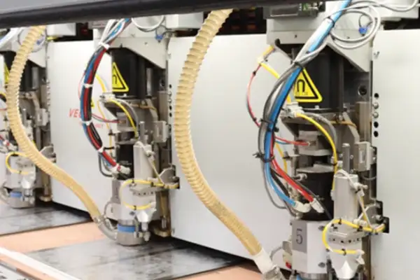
But guess what happened? It was precisely those two tiny ports that caused the entire production line to suffer from intermittent connectivity. After a thorough investigation, we discovered that the root cause lay in the device’s thermal resilience—although the equipment was nominally compliant with IEEE standards, certain components experienced performance degradation when operating continuously under the high-temperature conditions typical of a real-world industrial environment. This reminded me of a similar situation I encountered last year at a factory in southern China, where their network switches frequently suffered from signal attenuation during the monsoon season.
In reality, network deployment in industrial settings is a completely different ballgame compared to a standard office environment. Many people assume that simply meeting technical specifications is enough to ensure peace of mind; however, the factors that must be considered during actual operation are far more complex. For instance, the production line we are currently upgrading requires uninterrupted, 24-hour operation—a standard commercial-grade switch wouldn’t last even three months under such conditions.
Interestingly, a number of 2-port switches specifically optimized for industrial environments have recently appeared on the market. These devices feature not only ruggedized hardware designs but also firmware that has been specially tuned for industrial applications. One vendor even shared their test data with us: after operating continuously for 6,000 hours in a dust-laden environment, the performance degradation of their ports remained within a mere 3%.
However, I believe that when selecting such equipment, one shouldn’t rely solely on the technical specifications touted by the manufacturer. After all, environmental conditions vary from factory to factory—chemical plants must contend with corrosion issues, food processing plants need to manage temperature and humidity fluctuations, while mechanical processing plants like ours find vibration interference to be their biggest headache. Therefore, it is always best to conduct small-scale field trials first, allowing the equipment to run under actual operating conditions for a few weeks.
Speaking of which, that reminds me of an interesting case study: an automotive parts manufacturer, in an effort to cut costs, opted to use standard commercial-grade switches. The result was a millisecond-level delay in data synchronization across their entire assembly line. Although the delay per individual data packet was minuscule, the cumulative effect compromised the collaborative precision of their robotic arms. Once they switched to industrial-grade equipment, the problem vanished completely. This goes to show that in an industrial environment, the stability and precision of network equipment are absolutely not things to be taken lightly.
I now pay particular attention to network devices capable of maintaining stable performance even in harsh environments—after all, every single minute of downtime on a production line translates directly into a tangible financial loss. The new network switches I’ve tested recently demonstrate significant improvements in both thermal design and electromagnetic shielding. Some models can even operate reliably across an extreme temperature range—from -40°C to +85°C—which is truly impressive.
That said, even the finest hardware requires a well-conceived network architecture to deliver its full potential. We now tend to favor a distributed deployment strategy, configuring independent switching devices at each critical process node. This ensures that even if a single port fails, the overall system operation remains unaffected. While this design approach entails higher upfront investment, it proves to be more cost-effective and economical in terms of long-term operation.
While recently researching compact network devices, I observed an interesting phenomenon: whenever the topic of network switches comes up, many people instinctively assume that “the more ports, the better.” In reality, however, the optimal choice depends entirely on specific requirements.
I recall an instance where I was helping a friend debug an embedded system. At the time, the only switch I had on hand was a large-scale enterprise model; naturally, it simply wouldn’t fit inside the system’s cramped chassis. I subsequently switched to a compact, dual-port PCB-based network switch—and it solved the problem perfectly. The key advantage of these compact switches is that they don’t force you to pay for features you’ll never use—much like how you wouldn’t build an extra guest room in your house solely for the occasional visitor.
The ideal number of ports actually represents a delicate balancing act. I’ve seen far too many projects where the pursuit of an excessive number of network interfaces merely introduced unnecessary complexity. This is particularly true for latency-sensitive applications—such as the synchronized control of industrial robotic arms—where every additional forwarding hop introduces an increased risk of failure or delay.
During a test of a video transmission system, we discovered that switching to a simple dual-port configuration completely eliminated the video stuttering issues we had been experiencing. We later realized that our previous eight-port device—despite its powerful capabilities—was actually introducing a cumulative latency of several milliseconds when handling relatively low data volumes.
Nowadays, when designing compact IoT devices, I prefer to integrate the dual-port switching functionality directly onto the mainboard. This approach not only saves space but also reduces potential failure points associated with external connectors. In one smart home gateway project, for instance, simply by streamlining the network architecture in this manner, we were able to boost the system’s overall reliability by more than 30%.
Of course, this is not to say that multi-port switches are without value; rather, we simply need to select the appropriate tool for the specific scenario—much as you wouldn’t drive a heavy-duty truck just to run a quick errand to the grocery store.
I’ve always found the subject of network device selection to be particularly fascinating. Just the other day, while helping a friend set up the network cabling in their studio, this very topic came up in conversation once again. Their workspace is quite compact, yet they have a substantial amount of equipment—computers, printers, a NAS, and several security cameras—all crammed onto a single router. I’d suggest they give those little two-port PCB network switches a try.
Many people assume that the more ports, the better—but that’s not necessarily true. A two-port design actually results in cleaner cabling, cutting down on unnecessary tangles. This is especially true for models with metal casings; their heat dissipation is far superior to plastic versions, so you don’t have to worry about overheating even when they’re packed tightly into equipment racks.
Speaking of stacking capabilities, I think this is a truly underrated design feature. A single switch might seem simple on its own, but when you need to expand your network, the convenience of being able to simply stack units together is invaluable. You don’t have to reconfigure every single unit; you can just add more modules on top, much like stacking building blocks. This is particularly well-suited for situations where you’re starting small but anticipate future growth.
I once saw a similar setup at a factory where they used these types of switches to connect PLCs and control consoles. By using simple priority settings, they were able to guarantee the stability of critical data streams—a much more cost-effective solution than deploying complex, large-scale enterprise switches.
If you’re building your own equipment from scratch, the layout of the PCB is actually quite critical. Leaving sufficient space between components makes future maintenance much easier, and the placement of ventilation holes also impacts overall performance. These design details often prove far more practical than the raw numbers listed in a datasheet.
With the growing number of smart home devices—TVs, game consoles, smart speakers—all requiring network connectivity, a two-port switch can actually offer greater flexibility than a multi-port device. You can group devices that require high-speed data transfer onto a dedicated link, while routing less critical devices through standard connections.
I personally appreciate this minimalist design philosophy. Solving a problem doesn’t always require the most complex tools; sometimes, a perfectly balanced, “just-right” configuration proves to be the most robust and enduring solution.
I’ve recently been tinkering with a small project that requires a two-port network switch board. At first, I assumed it would be a pretty straightforward task—but it turns out there’s far more technical nuance involved than I had anticipated.
Just selecting the right chipset gave me a real headache for quite a while. On paper, the specs for all the mainstream solutions on the market look pretty much identical. Eventually, I realized that you can’t rely solely on the theoretical values listed in the datasheet; you actually have to build a prototype circuit and test it in the real world to verify its stability—particularly regarding heat generation during prolonged operation. The power consumption figures listed in datasheets are based on ideal laboratory environments, which turn out to be a completely different ballgame compared to how the device actually performs in practical use.
I also made a mistake during the PCB layout phase: I assumed a simple two-layer board would suffice. The result? Terrible signal integrity. I eventually had to switch to a four-layer board—specifically adding a dedicated ground plane—which significantly improved the situation. You really can’t cut corners when it comes to impedance matching. Being off by just a few ohms might not cause any issues during initial testing, but it creates a high risk of failure once you move into mass production. Port isolation is an easily overlooked aspect of design. I once conducted a test and discovered—to my surprise—that there was crosstalk occurring between two ports. After spending a considerable amount of time troubleshooting, I realized the issue stemmed from the layout: the components had been placed too close together. I subsequently adjusted the component placement to ensure sufficient spacing, and the problem was resolved. Such details are truly best learned through firsthand experience—by stumbling into the pitfalls yourself.
The choice of soldering process is also critical. On one occasion, I opted for a lead-free soldering process; however, during subsequent rework, the solder pads were damaged. Consequently, I now advise clients—particularly if manual debugging or rework is anticipated—to utilize lead-based soldering. Although it is less environmentally friendly, it offers superior reliability.
What gives me the biggest headache is firmware compatibility. I’ve found that the exact same hardware solution can perform vastly differently depending on the software environment version. I’ve since developed a habit: whenever a chip undergoes a revision, I perform a complete regression test. While this increases the workload, it effectively prevents a multitude of downstream issues.
Regarding cost control, I believe one shouldn’t focus solely on the unit price of the main chip. The cost of supporting components and manufacturing processes actually accounts for a significant portion of the total budget. Sometimes, selecting a slightly more expensive chip that requires a simpler peripheral circuit can actually result in a lower overall cost; this requires a comprehensive, holistic assessment.
I now tend to favor established, market-proven chip models. While they may not offer the absolute latest performance metrics, they provide greater assurance regarding stability and supply availability. This is particularly crucial for industrial-grade applications, where reliability takes precedence over benchmark scores.
Designing compact circuit boards—especially small-form-factor ones—is the ultimate test of one’s overall layout proficiency. The challenge lies in how to logically arrange various functional modules within a confined space while simultaneously maintaining signal integrity. Finding the optimal solution invariably requires multiple iterations of adjustment and refinement.
With the completion of every new hardware revision, I feel as though I’ve gained fresh insights. Such is the nature of hardware design: there are always new challenges waiting to be solved. Yet, it is precisely this continuous process of problem-solving that makes the field so captivating.
I recall the first time I had to select networking hardware; I was particularly vexed by the issue of port count. I was working on a smart home project that required networking devices across two distinct zones. Standard off-the-shelf 5-port switches were too bulky, while single-port converters were insufficient for the task. Then, quite by chance while browsing an electronics market, I stumbled upon a 2-port PCB-mounted network switch module. It was roughly the size of a cigarette lighter and could be directly embedded within the device enclosure. This compact design made me realize that “more ports” isn’t always better; the key is to align the port count with the specific requirements of the actual application scenario.
Nowadays, many IoT devices are adopting this miniature switch solution. For instance, in a recent environmental monitoring system I designed for an agricultural greenhouse, each data acquisition node only needed to connect to two peripherals—a soil sensor and a weather station. By utilizing a 2-port PCB network switch, we were able to eliminate the need for an external switch, thereby simplifying the system and avoiding the associated hassle. However, when selecting components, it is crucial to pay attention to the differences between various chip solutions; while some industrial-grade chips come with a higher price tag, they are capable of withstanding the temperature fluctuations inherent in outdoor environments.
The impact of PCB layout on performance is often far greater than one might imagine. During one testing phase, we observed erratic network latency—fluctuating wildly between high and low values. We eventually traced the issue back to power supply traces running too close to the differential signal lines. By subsequently switching to a four-layer board design—thereby completely isolating the analog and digital sections—the problem was resolved. Such nuances are rarely emphasized in official documentation and often require hands-on experimentation to discover.
In reality, the primary advantage of a dual-port switch lies in its flexibility. During a recent renovation of an older office building, we encountered a situation where the placement of network ports in each room was irregular; using standard switches would have necessitated the installation of a vast amount of additional cabling. Instead, we deployed wireless access points (APs) equipped with built-in switches in every room, utilizing their two ports to connect—one to the in-wall network cable and the other to peripheral devices. This approach not only reduced costs but also significantly improved network coverage. While this specific application is rarely mentioned in traditional networking tutorials, it proves to be a highly practical solution in real-world engineering projects.
Temperature adaptability is often overlooked. On one occasion, after a product was shipped to a client in the southern region, it began experiencing frequent connection drops. After an extensive investigation, we discovered that the issue stemmed from the instability of standard commercial-grade chips operating in a high-temperature environment. The problem was immediately resolved once we switched to industrial-grade chips and added additional ventilation ports. Consequently, whenever I am selecting components now, I pay particular attention to the operating temperature range—a factor I consider even more critical than the theoretical performance specifications listed in the datasheet.
I believe the true value of miniature network switches lies in their ability to redefine the possibilities of network topology. Much like LEGO bricks, these modular building blocks allow network structures to align seamlessly with actual physical layouts, rather than forcing the on-site environment to accommodate rigid equipment specifications. This shift in design philosophy holds far more significance than the mere pursuit of technical parameters.
I’ve always found the design of network equipment fascinating. I recently assisted a friend’s company with a small project involving a two-port PCB-based network switch module; it was then that I realized these seemingly simple devices actually harbor a surprising amount of technical sophistication.
What appeals to me most about these little gadgets is their flexibility. You can embed them directly into a wide variety of devices to suit your specific needs, without being constrained by the physical form factors of off-the-shelf switches. For instance, a client once required data segregation inside their surveillance cameras; we simply integrated one of these switch modules directly onto the camera’s mainboard, thereby eliminating the hassle of installing external networking hardware.
Speaking of management capabilities, I feel many people underestimate the configuration potential of small-scale switches. Even basic models can achieve effective traffic isolation through simple VLAN settings. On a previous project for a design studio—where they needed to segregate their video production equipment from their general office network—we utilized port-based VLAN functionality, and the results were surprisingly excellent.
While thermal management certainly requires consideration, there is no need to over-engineer the solution. Several projects I’ve overseen have demonstrated that, provided the layout is sensible, passive cooling (natural convection) is entirely sufficient for standard operating environments. The key is to leave adequate clearance for airflow, rather than cramming components together in a dense, tightly packed arrangement.
What has surprised and delighted me most is the high degree of customization now available for these types of modules. Everything from firmware to physical interfaces can be tailored to specific requirements; models that support remote management, in particular, can significantly reduce the time and effort required for on-site maintenance. That said, the choice ultimately depends on the specific scenario; in some environments, a basic, “plug-and-play” version may actually be the more appropriate and practical choice.
In my view, the most critical aspect of selecting this type of equipment is clearly defining your actual operational needs, rather than blindly chasing after high-end features. More often than not, a simple solution proves to be the most reliable one—especially for non-technical users, where ease of maintenance should always be the primary consideration.
While recently working on the network layout for a small design studio, I observed an interesting phenomenon: the massive, multi-port switches—often boasting dozens of ports—that dominate the market certainly grab one’s attention. However, what truly caught my eye and impressed me were the unassuming little two-port units—specifically, those compact switch modules designed for direct integration onto a circuit board. This type of design is actually particularly well-suited for scenarios like ours—situations where space is limited, yet a stable connection is absolutely essential. For instance, I’ve used it to directly link my studio’s surveillance cameras to a NAS storage unit. This approach not only bypasses the need for data to traverse complex network paths but also guarantees the stability of the video stream transmission. What surprised and delighted me most was how effectively it manages heat dissipation.
I recall a time when I helped a friend overhaul his smart home system. We installed these two-port switch modules in every room. The result was a system-wide response speed that was significantly faster than when we were using traditional network switches. This was especially noticeable with smart devices requiring real-time feedback; they no longer suffered from any lag or stuttering issues.
In reality, the potential applications for these compact switches are far broader than one might initially imagine. I’ve seen them deployed in in-vehicle systems, and I’ve also observed automated factory equipment utilizing this compact design to establish direct, device-to-device connections. The key to success lies in selecting the appropriate PCB material and manufacturing processes.
I personally tend to favor boards that incorporate a “thick copper” design. Although this does entail a slightly higher manufacturing cost, it proves to be far more reliable in environments subject to significant temperature fluctuations. Component spacing is another critical factor; if components are packed too densely, it significantly increases the likelihood of operational issues.
Nowadays, many manufacturers are busy touting all sorts of flashy, novel features. However, based on my own experience, when it comes to two-port switch modules, stability reigns supreme. After all, these devices are frequently deployed in locations where regular maintenance is difficult or impractical. Rather than chasing after superfluous, bells-and-whistles features, it is far wiser to focus on building a solid, robust foundation.
I’ve always found the field of network hardware design to be fascinating. This is particularly true for those diminutive 2-port PCB network switches; while they may appear simple on the surface, they involve a surprising amount of technical nuance and expertise. Many people tend to dive straight into worrying about trace routing and grounding schemes; however, I believe the more prudent approach is to first clearly define the specific operating environment in which the device will be deployed.
Take, for instance, the industrial-grade switch we designed recently: whenever the heavy-duty motors in the workshop fired up, the entire electrical grid would experience significant voltage fluctuations. In such an environment, fixating solely on the precise routing of differential pairs can easily lead one to overlook far more critical, systemic issues. Of course, I’m not suggesting that differential routing is unimportant—quite the contrary. In fact, such challenging environments serve as the ultimate test of a designer’s true technical prowess. You must ensure that the signal remains clear and uncorrupted amidst the electrical noise; achieving this requires incorporating sufficient design margins and headroom during the PCB layout phase.
The transformer is a component that is often treated merely as a generic, off-the-shelf part; however, its specific placement on the board can have a profound impact on the entire circuit’s electromagnetic characteristics. My personal workflow involves first locking down the precise positions of the transformer and the RJ45 connector, and then arranging the remaining components around those fixed points. Some designers prefer to place a copper pour beneath a transformer; however, I believe this actually introduces unnecessary coupling.
Speaking of power supply sections, I’ve noticed that many novices tend to over-engineer them. Not every application requires a complex filtering network; sometimes, a simple LC circuit proves to be far more reliable. The key lies in adjusting parameters based on actual load variations, rather than blindly applying textbook formulas.
Another critical aspect is interface design. Stackable switches may sound impressive in theory, but if the interfaces are not properly managed, stacking them can actually lead to mutual interference. I personally prefer to position stacking interfaces along the edges of the PCB and isolate them using a dedicated ground plane.
In reality, the greatest pitfall in this type of design is rigid adherence to convention. Every project presents a unique set of requirements, and simply recycling previous solutions often proves ineffective. I prefer to approach each new project as an opportunity for exploration—venturing beyond standard practices to experiment with fresh ideas. After all, in the field of electronics design, there are always new frontiers waiting to be discovered.
The performance bottleneck of an RF front end is rarely the chip
A poorly designed Servo Controller PCB can lead to motor jitter, overheating,
When data centers upgrade their GPUs, the real bottleneck often hides in
- Experte für die Produktion kleiner bis mittlerer Chargen
- Hochpräzise PCB-Fertigung und automatisierte Montage
- Zuverlässiger Partner für OEM/ODM-Elektronikprojekte
Geschäftszeiten: (Mo-Sa) von 9:00 bis 18:30