
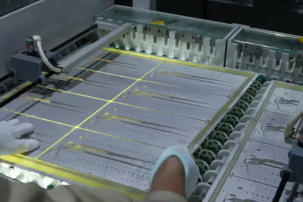
Industrial Relay Control Board PCB: What Textbook Calculations Miss About Real-World Failure
A relay control board that works perfectly in the lab can fail
I have always felt that splitting the procurement of PCB manufacturing and assembly into separate tenders is a rather risky practice. On the surface, it appears to save a bit of money, but in reality, it harbors a headache-inducing number of hidden pitfalls. I recall visiting a friend’s factory once; they were in the midst of dealing with a batch of boards plagued by poor soldering—a compatibility issue stemming precisely from the decision to engage different suppliers for fabrication and assembly.
Those PCB manufacturers who aggressively market themselves on the basis of low prices often cut corners in areas you cannot easily see. For instance, they might skimp on the thickness of the solder mask or use cheap, inferior ink. These subtle defects may not be apparent during standalone testing, but they are exposed in full view the moment the boards hit the SMT assembly line. This is particularly problematic when paired with highly active solder pastes; an incompatible solder mask can lead to poor wetting, resulting in solder bridging (short circuits) or cold joints (poor electrical connections).
The most textbook example I’ve encountered involved a smart home device manufacturer. To cut costs, their PCB supplier applied an unusually thin solder mask layer, while their assembly house opted for a highly active solder paste. The result? During the reflow soldering process, the active solder paste penetrated the thin solder mask layer, causing short circuits between adjacent pins. The entire batch of products had to be completely reworked—a remedial cost that far exceeded the meager savings originally gained through the separate procurement strategy.
In truth, competent PCB manufacturers will tailor their production parameters to align with the customer’s subsequent assembly processes. They take into account factors such as the solder mask’s thermal resistance, surface flatness, and even how its color might impact subsequent automated optical inspection (AOI) during assembly. All these intricate details require close communication and coordination with the assembly house during the initial design phase—yet under a split-procurement model, achieving this level of synergy becomes virtually impossible.
Even more complicated is the selection of the surface finish process. For instance, certain specialized applications require an Electroless Nickel Immersion Gold (ENIG) surface finish; however, if a PCB manufacturer opts for Hot Air Solder Leveling (HASL) instead—simply to cut costs—it can lead to soldering defects during the assembly stage. It is all too common for two separate suppliers to play the blame game, and ultimately, it is the purchasing party that bears the brunt of the loss.
Nowadays, an increasing number of manufacturers are beginning to prioritize the holistic coordination between manufacturing and assembly. After all, assigning accountability when issues arise can be a cumbersome process; it is far more prudent to select a partner capable of providing end-to-end services right from the start. While the unit cost may be slightly higher, this approach spares you a great deal of subsequent headaches and complications.
In my years of working with PCBs, my greatest realization has been this: do not artificially decouple the manufacturing process from the assembly process. Many people assume that sourcing these services separately will either save money or allow them to handpick superior suppliers. However, the reality is often quite different: while the PCB manufacturer is still fabricating the boards, the assembly plant on the other end is already clamoring for materials. Misaligned schedules between the two parties are a frequent occurrence.
I recall a specific project where the circuit boards were technically finished, yet the entire process stalled for a week due to logistical bottlenecks. The assembly plant had already scheduled its production lines, leaving them no choice but to sit idle. This approach—which ostensibly offers greater flexibility through separate management—actually tends to disrupt the overall workflow. Moreover, should any issues arise, it creates an environment where both parties are quick to deflect blame onto one another.
In truth, the greatest pitfall within the PCB manufacturing and assembly workflow is the existence of information gaps. The board manufacturer understands how the boards are fabricated but remains unaware of the specific challenges that might arise during assembly; conversely, the assembly plant is well-versed in production processes but possesses only limited knowledge regarding the specific characteristics of the PCB substrate materials. I have personally encountered situations where a failure to properly communicate the substrate’s Glass Transition Temperature (Tg) value resulted in slight deformation of the boards during the reflow soldering process.
Consequently, I now prefer to seek out partners capable of delivering comprehensive, holistic solutions. This does not necessarily mandate a “one-stop shop” approach, but it does require—at the very least—the establishment of a robust and seamless communication framework. An effective purchasing professional should focus their energy on facilitating technical alignment during the initial planning stages, rather than spending their days chasing after logistics updates.
Ultimately, in the realm of hardware product development, every stage is inextricably linked. Artificially segregating PCB manufacturing from assembly serves only to inflate communication overheads and heighten operational risks. While such a separation may appear—on the surface—to yield minor cost savings, it often merely sows the seeds for far more significant complications and latent issues further down the line.
During a recent conversation with an old friend who works in the hardware sector, I observed an intriguing phenomenon: many people today tend to oversimplify the complexities of PCB manufacturing. They operate under the assumption that they can simply hand over their design files to a board manufacturer and consider the job done. In reality, however, the true determinants of a finished product’s quality are often those subtle details—the very elements that are most easily overlooked. For instance, our team once nearly stumbled while designing a board featuring a BGA package. At the time, our circuit engineers—following standard practice—opted for a 4-layer board stackup. However, during a design review meeting, a veteran engineer suddenly asked: “Have you calculated the coefficient of thermal expansion for the BGA region?” Everyone was stunned into silence on the spot—this is a parameter that one typically wouldn’t think to look up specifically.
We later discovered that standard FR4 material expands at a significantly higher rate than BGA chips when subjected to high temperatures. Had we proceeded with standard soldering processes regardless, the solder joints would have been subjected to such extreme stress during cooling that they would have inevitably cracked. This incident taught me a valuable lesson: when selecting a PCB manufacturer, one cannot simply look at the price list; one must verify their willingness and capability to collaborate on material selection and compatibility.
Nowadays, many small-to-medium-sized PCB manufacturers find themselves in a rather passive position. Clients invariably want to achieve the best possible performance at the lowest possible cost—yet some of these requirements are inherently contradictory. For example, a client might demand the stability and reliability of an ENIG surface finish while only budgeting for the cost of OSP. In such situations, some manufacturers might secretly substitute the specified surface finish process.
The most egregious case I’ve ever witnessed involved a consumer electronics product. The assembly plant adjusted its reflow soldering temperature profiles three times—specifically calibrated for an ENIG finish—yet issues persisted. Upon final teardown and inspection, it was revealed that the PCB manufacturer had actually used a modified version of OSP. This kind of information disconnect is almost inevitable within a fragmented procurement model.
Ultimately, hardware development is a systems engineering endeavor. From the initial design phase through PCB manufacturing and assembly, a continuous flow of technical information and handoffs is required. Yet, a common scenario in the industry today is for design teams to simply “dump” their Gerber files onto the manufacturer and assume that their work is done.
The truly reliable approach is to involve the PCB manufacturer in the design review process early on—particularly when dealing with fine-pitch BGAs. Last year, for instance, we managed to avert significant financial losses on a project precisely because we brought the manufacturer in early to assist with impedance calculations.
Sometimes I feel this industry needs more cross-disciplinary communication. Designers need to understand the practical boundaries of manufacturing processes, while process engineers need to grasp the original design intent. After all, no one wants to see the board they designed end up as scrap on the assembly line.
Of course, this can be a challenge for small teams; consequently, I now prioritize PCB manufacturers that offer collaborative engineering services. While their rates might be 10% higher, the savings realized by avoiding costly rework and scrap make it an investment that is absolutely worth the price.
I have seen far too many teams stumble on their PCB development journey. They spend a fortune hiring a top-tier manufacturer to fabricate their boards, only to discover during the assembly phase that the solder pads have oxidized—rendering the entire batch of boards fit only for the scrap heap. What makes matters even more frustrating is that when you confront the PCB manufacturer, they simply whip out a test report proving that all parameters met specifications upon shipment. Then, when you turn to the assembly plant, they adamantly insist that their soldering process is flawless. This kind of finger-pointing drama has become practically the norm in the industry.
So, where does the actual problem lie? Many people treat PCB fabrication and assembly as two entirely separate orders. The board manufacturer considers their job done the moment they deliver the goods; they couldn’t care less whether components can actually be soldered onto the boards later on. Meanwhile, the assembly plant performs only basic incoming material inspections; as long as the boards show no obvious physical damage, they proceed with production as usual. The result of this “every man for himself” mentality is a litany of defects during the SMT process—solder bridging and cold joints abound—ultimately leading to a storm of complaints about the final product once it hits the market.
A hardware team I know learned this lesson the hard way last year. They were designing a smart home motherboard that required buried vias, so they specifically sought out a PCB manufacturer renowned for precision fabrication. However, once the boards arrived at the assembly plant, they discovered that—due to a substandard copper plating process—half of the vias burst open during reflow soldering. To make matters even more dramatic, the board manufacturer produced IPC standards to prove that the copper thickness in the vias met specifications, while the assembly plant adamantly maintained that their temperature profile adhered to all guidelines. This order, valued at 200,000 RMB, ultimately ended with the client canceling the contract.
Nowadays, an increasing number of companies are seeking out suppliers that offer end-to-end, integrated services. This isn’t necessarily about choosing the most expensive option; rather, when you bundle both fabrication and assembly with a single vendor, they are compelled to take full responsibility for the final finished product. A drone manufacturer I visited last week left a deep impression on me: their engineers are permanently stationed at their partner factory, participating in every step of the process—from board material selection to SMT debugging. The batch of flight control boards they recently mass-produced achieved a first-pass yield of 98%—significantly higher than the industry average.
Some people mistakenly believe that splitting procurement between different vendors saves money, but in reality, the hidden costs are far higher. You have to hire additional personnel just to coordinate between the two suppliers, and whenever issues arise, you have to organize three-way meetings to resolve them. Not to mention the time costs involved—I once spent half a month exchanging emails back and forth over an impedance dispute, only to discover in the end that the stack-up structure provided by the board manufacturer deviated from the actual production reality. Had the entire process—from design through assembly—been managed within a single integrated system, such a rookie mistake would never have occurred.
Of course, there are always exceptions. For instance, if you require military-grade circuit boards involving highly specialized processes, it might indeed be necessary to seek out separate, top-tier specialist manufacturers for each specific task. However, for the vast majority of consumer electronics products, rather than acting as a referee between separate manufacturers and assembly houses, it is far more practical to find a partner capable of handling the entire process end-to-end. After all, what we ultimately need are reliable, functional circuit boards—not just a stack of inspection reports where everyone is busy shifting blame.
I feel that many people today focus too heavily on superficial details when selecting a PCB supplier. Everyone tends to ask the same standard questions: “How much inventory do you hold?” “Do you have the necessary licensing agreements?” “Can you source alternative components?” While these questions are certainly important, they often cause people to overlook the more fundamental aspects of the process. I have witnessed numerous projects collapse completely simply because a supplier failed to deliver on the basic, foundational stages.
A truly reliable PCB manufacturing and assembly service should embody a sense of genuine integrity at every stage—much like a seasoned craftsman approaching a woodworking project. Take, for example, a factory we partnered with last year: instead of boasting about the sheer number of AOI machines they owned, they proactively shared their detailed testing protocols with us right from the prototyping phase. It is precisely these kinds of details that instill confidence; they were so meticulous that they would perform triple-calibrations for even a minute impedance deviation of just 0.1 ohms—demonstrating an attention to detail that surpassed even our own requirements as the design team.
This level of rigor is even more critical during the procurement phase. Some suppliers pay lip service to “digital transparency,” yet the moment you press them for specific delivery timelines for materials, they resort to evasive stalling tactics. A truly effective partner, however, will directly connect you with their procurement manager—sharing their contact details—so you can track exactly which original manufacturer your components are shipping from, and even monitor customs clearance progress in real-time. This level of open transparency is far more valuable than any mere verbal promise.
Speaking of testing, nothing frustrates me more than suppliers who treat X-ray inspection as nothing more than a marketing gimmick. Truly valuable testing is that which is integrated throughout the entire workflow—from establishing a quality baseline during the bare-board stage to conducting stress tests that simulate real-world operating conditions after assembly. On one occasion, we encountered a baffling memory read/write anomaly; the supplier’s engineers worked through the night, performing over thirty Functional Tests (FCTs), until they finally traced the issue back to a mere 0.5-degree fluctuation in the soldering temperature profile. It is this level of relentless dedication to precision that constitutes true core value.
The industry today loves to talk about “Industry 4.0,” but I firmly believe that even the most sophisticated automated systems can never truly replace the sense of personal responsibility and diligence found in human beings. Just last week, a new supplier attempted to skip the impedance testing phase in a rush to meet a deadline; we immediately put a stop to it. They fail to understand why we obsess over such “minor details.” In reality, a circuit board is akin to the foundation of a house; if even a single brick isn’t laid correctly, the entire structure could collapse.
Ultimately, selecting a partner boils down to whether they treat quality as a creed—a core belief—rather than just another line item on a project budget spreadsheet. An exceptional PCB service provider should operate much like a seasoned traditional Chinese medicine practitioner: capable of both precisely diagnosing existing issues and anticipating potential risks. That is the mark of a relationship worthy of long-term trust.
I have witnessed numerous companies get thoroughly put through the wringer during the PCB manufacturing and assembly phases. Despite engaging suppliers within the very same industry, they find themselves constantly shuttling back and forth to coordinate efforts; the errors stemming solely from information transmission are enough to give anyone a headache. Sometimes, the boards are fully fabricated only for issues to surface regarding component compatibility or improperly calibrated soldering parameters—necessitating yet another round of prototyping.
Truly reliable, fully integrated service providers are actually quite rare; the key lies in whether their internal workflows are genuinely interconnected. While some companies may offer both PCB manufacturing and assembly services, their manufacturing department and assembly team often operate as two entirely distinct entities, making internal communication feel no different than collaborating with a separate external firm.
What I value most is the ability to intervene early—specifically during the design phase. A robust PCB design should account for subsequent assembly processes right from the outset, rather than having each party work in isolation and simply hoping to iron out the kinks later on. I recall a previous project where the designer set the spacing between solder pads to an extremely tight tolerance; although the board could technically be manufactured, the assembly yield rate remained stubbornly low during the surface-mount process. We subsequently switched to a service provider capable of offering design consultation, and they were able to flag this specific issue while the schematics were still being drafted.
Supply chain integration is equally critical. Given that component lead times are currently prone to frequent extensions, managing PCB manufacturing and material procurement separately often results in a frustrating cycle where the boards sit idle waiting for components, or vice versa. A truly integrated service provider will holistically coordinate these two domains—going so far as to adjust production schedules based on real-time component inventory levels.
The continuity of the testing phase is another aspect that is frequently overlooked. Some manufacturers relegate testing to the very final step; consequently, when issues are eventually detected, it becomes incredibly difficult to trace whether the root cause lies in the PCB’s manufacturing quality or the assembly process itself. I tend to favor service providers who strategically embed inspection checkpoints after every critical process step, as this allows for much faster identification of the problem’s source.
In fact, there is a very simple litmus test for gauging the true degree of integration: observe whether they have the confidence to consolidate their quality assurance guarantees for both manufacturing and assembly into a single unified document. If they still require you to sign two separate quality agreements, it serves as a clear indication that their internal coordination and synergy are not yet up to par. A truly well-integrated service provider takes full responsibility for the entire process from start to finish, rather than leaving the client to shuttle back and forth between different departments, resolving disputes on their own.
Many service providers on the market today emphasize “integration,” yet very few actually achieve seamless connectivity. In my view, the key factor is not the quantity of equipment they possess or the scale of their operations, but rather the fluidity of their internal information flow—whether their various departments are truly working in unison toward a common goal.
I have seen far too many teams stumble during the PCB manufacturing and assembly stages. They often assume that unbundling the procurement process will save them money. In reality, however, this fragmented approach frequently leads to even more problems. Just think about it: synchronizing delivery schedules across different suppliers is incredibly difficult. A delay in just a single component can bring the entire production line to a grinding halt. Few people ever factor these “hidden costs” into their calculations.
I recall one instance where a project of ours nearly collapsed simply because the supplier for basic components—such as resistors and capacitors—unexpectedly reneged on their agreement at the last minute. That was the moment I truly realized the critical importance of integrated services. The real value lies not in the unit price of individual items, but in the smooth, uninterrupted operation of the entire supply chain. Consequently, for every project I oversee now, I insist on partnering with a service provider capable of integrating both manufacturing and assembly.
Many people focus excessively on the unit cost of components while overlooking the associated communication and time costs. Imagine having to interface simultaneously with five or six different suppliers; you could easily spend two hours a day doing nothing but coordinating progress updates—and that’s before even accounting for the time spent wrangling over quality disputes. An integrated service provider, by contrast, offers a comprehensive, end-to-end solution—handling everything from raw material procurement to final product testing.
I recently came across a very telling case study: a friend’s company, in an attempt to save a small amount of money, adopted a fragmented procurement model—only to suffer significant losses as a result. Subtle variations in the parameters of different batches of base materials caused functional instability across the entire batch of finished boards. Such issues simply would not arise with an integrated service provider, as they maintain rigorous quality control throughout the entire production workflow.
In my opinion, selecting a PCB service provider is akin to choosing a business partner: one must evaluate their overall capabilities rather than simply comparing quotes for individual stages of the process. After all, what we ultimately need is a reliable, finished product—not just a pile of parts waiting to be assembled.
Those truly in the know understand that high-quality PCB manufacturing and assembly services should function like a symphony orchestra, where every single stage operates in perfect, seamless harmony. A fragmented procurement model—much like asking musicians to practice in isolation and then attempt to play together without rehearsal—yields results that are all too predictable.
Nowadays, I place a premium on a supplier’s integration capabilities, as this directly dictates the final quality of the product. Those procurement costs that appear to have been “saved” upfront often come back to haunt you later, exacting a double penalty in various forms.
After years of working in hardware development, I have increasingly come to believe that instead of agonizing over procurement details, one’s energy is better spent on product design. Manufacturing and assembly tasks should be entrusted to professional integration service providers; this is, without a doubt, the most efficient way to work.
I have seen far too many teams stumble when it comes to PCBs. They often operate under the misconception that separating manufacturing from assembly—by engaging different suppliers for each—will save them money. The result? When issues inevitably arise with the boards, the two parties simply play the “blame game,” passing the buck back and forth. The PCB manufacturer claims the soldering is at fault, while the assembly house insists the raw board material is defective. Ultimately, the client is the one left holding the bag—forced to foot the bill for destructive testing just to pinpoint the root cause.
In reality, industry insiders who truly know their craft have long since shifted toward integrated manufacturing. With this approach, a single cohesive team considers every subsequent stage of the process right from the initial design schematics. For instance, a client recently approached us regarding a high-frequency PCB project. We proactively adjusted the copper thickness parameters during the schematic design phase; this not only ensured signal integrity but also made it significantly easier for the factory to maintain precise etching tolerances during production.
Some clients worry that relying on an integrated service provider might lead to monopolistic pricing. However, the reality is quite the opposite. When you package the entire workflow—from PCB manufacturing to assembly—and entrust it to a professional, integrated team, you actually eliminate a massive amount of communication overhead and avoid the hidden costs associated with quality-related disputes.
One case that particularly struck me occurred last year during a smart wearable project. The client had originally engaged four separate vendors to handle flexible PCB production, component procurement, and SMT assembly, respectively. The result? A staggering 30% of the initial sample batch suffered from cold solder joints. When they subsequently brought the project to us, we had to completely recalibrate every parameter—from the choice of base materials to the solder paste formulation—only to discover that the design of the heat dissipation vias was interfering with the optimal soldering temperature profile.
An increasing number of clients are now recognizing the inherent risks of fragmented procurement. While selecting the lowest-cost option for each individual stage might seem prudent on the surface, it effectively strips you of control over the entire quality chain. The true value of integrated manufacturing lies in empowering experts to tackle challenges through a holistic, systems-oriented lens—an approach that is infinitely more meaningful and effective than merely comparing unit prices in isolation.
I recently had a conversation with a friend who works in the smart home sector. He mentioned that his company has historically adhered to the traditional, fragmented procurement model—contracting one factory for PCB fabrication and a completely different one for assembly. This time, however, they ran into a major crisis: after the PCBs were manufactured, significant defects were only discovered much later—during the testing phase at the assembly facility. The initial design was poorly thought out; there were simply too few test points available on the board to accommodate a bed-of-nails fixture. The team at the assembly plant took one look and shook their heads, explaining that automated test equipment was out of the question—we would have to switch to the much slower, manual process of flying probe testing instead. Do you realize what that implies? Not only did it drastically extend our timeline, but our costs skyrocketed exponentially.
Even more vexing was the issue of supply chain coordination. Whenever a problem arose, we were forced to shuttle back and forth between the PCB manufacturer and the assembly house, with each side offering conflicting narratives. The board manufacturer maintained they had executed the build exactly according to the schematics, while the assembly plant insisted that the lack of test coverage was a direct result of design limitations. Caught in the middle, we felt like nothing more than mere intermediaries.
In reality, this entire situation could have been completely avoided. We subsequently adjusted our strategy, bringing both the PCB supplier and the future assembly partner into the design phase right from the very beginning. Specifically, we had all three parties jointly review the Design Rule Checks (DRC)—particularly for high-density BGA regions and power management circuitry.
Our current protocol requires the PCB manufacturer to complete basic continuity testing and impedance control reporting before delivery. This ensures that when the boards reach the assembly stage—and undergo subsequent ICT or flying probe testing based on the actual component placement—the entire process proceeds far more smoothly.
Ultimately, the biggest pitfall of this decentralized procurement model isn’t the technology itself, but rather the hidden costs stemming from information silos. You may end up spending several times the amount of time simply trying to bridge the communication gap—and even then, there is no guarantee that the underlying issues will be fully resolved. Having worked in this industry for many years, I’ve observed a rather interesting phenomenon: many people assume that separating PCB manufacturing from assembly—by sourcing each from a different vendor—will save them money or result in superior workmanship. In reality, however, the process is far more complex than they imagine.
I’ve seen countless projects where, in an initial bid to drive down costs, a client selects a cheap PCB fabrication house, only to later engage a separate assembly plant that offered a favorable quote. The moment the two parties attempt to interface, problems inevitably arise. The surface finish on the PCBs might not be compatible with the assembly plant’s solder paste; consequently, no matter how the reflow oven temperature profile is adjusted, the results remain suboptimal. During the small-batch trial production phase, the yield rates can be alarmingly low. At this juncture, attempting to mediate between the two vendors becomes an incredibly arduous task. The fabrication house insists their processes are flawless and meet industry standards, while the assembly plant maintains that their parameters are set to standard configurations. The entire project grinds to a halt as time is wasted on endless finger-pointing and disputes. Ultimately, when factoring in the project delays and the costs of rework, the total expense ends up being far higher than if they had simply engaged a reliable, one-stop service provider from the very beginning.
Sometimes, the issue isn’t that the vendors lack the desire to do a good job; rather, the inherent flaw lies in this fragmented division of labor itself. PCB design is a holistic process—from the selection of base materials to the final component placement and testing—where every stage is intricately interconnected. When the process is fragmented, each vendor focuses solely on their specific segment, leaving no single party to assume full responsibility for the quality of the final product. If issues arise, you are forced to act as a go-between, shuttling information back and forth between the parties like a human relay. In the process of transmission, the original intent often gets distorted. For instance, the impedance control specifications articulated by the PCB designer might be interpreted according to a different set of standards by the fabrication house. Similarly, the assembly plant might adjust the reflow oven temperature based on their general experience, unaware that the specific PCB material being used has a unique coefficient of thermal expansion—a compatibility issue that remains undetected until the final functional testing fails.
Furthermore, the notion that sourcing manufacturing and assembly separately offers greater flexibility to switch vendors is rather naive. While doing so might save a small amount of money once or twice, the value derived from the mutual understanding and deep operational synergy fostered through a long-term partnership far outweighs that marginal cost difference. A truly effective partner will proactively help you mitigate risks in advance. For example, an assembly plant familiar with your product’s specific characteristics might recommend that the fabrication house enhance heat dissipation in certain areas; conversely, the fabrication house might adjust the solder mask openings to better accommodate the specific component placement process. These types of nuanced optimizations—which are critical to success—simply cannot be achieved by a hastily assembled, ad-hoc team of vendors.
Ultimately, selecting a vendor is not like grocery shopping where you simply pick the cheapest option available—especially in a field like PCB manufacturing, which involves a high degree of technical integration. The small amount of money you might save upfront could very well end up being squandered on communication overheads and the costs of mitigating unforeseen risks. It is far more prudent to engage a partner capable of overseeing the entire process from the outset; even if the unit cost is slightly higher, the peace of mind and the assurance that your project will proceed smoothly are invaluable—surpassing the importance of any other factor.
A relay control board that works perfectly in the lab can fail
A medical pump PCB that performs flawlessly in the lab can produce
The ADAS controller PCB is no longer a passive substrate — it
- Experte für die Produktion kleiner bis mittlerer Chargen
- Hochpräzise PCB-Fertigung und automatisierte Montage
- Zuverlässiger Partner für OEM/ODM-Elektronikprojekte
Geschäftszeiten: (Mo-Sa) von 9:00 bis 18:30