
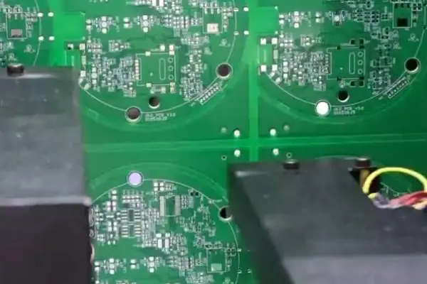
Why the Circuit Board Beneath the Camera Determines Whether Your Surveillance System Holds Up for Years
When selecting components for a security monitoring system, most attention goes to
Recently, while tinkering with Megtron PCBs in the lab, a question suddenly occurred to me: We are always pursuing higher wiring density and faster signal transmission speeds—but sometimes, do we overlook the most basic things? For example, that seemingly insignificant drilling process.
I remember once testing a high-frequency board and finding that the signal attenuation was particularly severe. After much investigation, I discovered the problem lay in the quality of the walls of several micro-vias. The laser drilling equipment I was using hadn’t been properly calibrated, resulting in slight burrs on the hole walls. While almost invisible to the naked eye, these burrs were enough to affect the uniformity of subsequent metallization. This incident made me realize that drilling precision isn’t just a numbers game; it directly impacts the electrical performance of the entire board.
Many people believe the key to PCB design lies in the number of layers or material selection, but I think the reliability of hole metallization is the hidden key to success. Especially with high-speed materials like Megatron, uneven copper plating within the holes, even with a perfect circuit design, will significantly compromise signal integrity. I’ve seen engineers cut corners on post-drilling cleaning to meet deadlines, resulting in intermittent board failures six months later.
Now, when working on high-density boards, I prefer to spend time verifying the drilling process. For example, I test the lifespan of different drill bits on prototypes and record the trends in hole wall roughness. Although it takes two extra days, it’s well worth the investment compared to scrapping an entire batch of boards during mass production.
There’s an interesting phenomenon: when producing 20-layer PCBs, some factories prefer mechanical drilling followed by plasma cleaning, while others insist on laser drilling plus chemical desmearing. Both methods can meet standards, but the long-term reliability of the final product differs significantly. I tracked a batch of boards used in communication base stations, and after three years, the failure rate of the laser-drilled boards was significantly lower—because the thermal expansion coefficient of the hole walls is more stable.
Ultimately, PCBs are like building foundations; the quality of the drilling is the steel framework within the foundation. You can build a beautiful building on the ground, but if the framework is flawed, problems will inevitably arise. Especially now, with the rapid pace of equipment iteration, the lifespan of a single board can determine the market reputation of the entire product.
Recently, I’ve been trying to move the drilling quality inspection point to the beginning of each production batch instead of waiting until the final sampling inspection. Although it increased costs slightly, the number of problems reported on the production line has indeed decreased. This attention to detail may be more meaningful than pursuing the latest materials.
I’ve always felt that many discussions about high-end PCBs focus too much on technical parameters. Last year, during a visit to a factory, I saw the Megtron PCB production line and realized that what truly determines a product’s lifespan is often the seemingly insignificant choice of materials. The engineers weren’t repeatedly emphasizing any mysterious formula, but rather how the stability of the basic materials affects the entire system.
An interesting phenomenon is that many manufacturers, in pursuit of ultimate signal transmission speeds, focus on reducing dielectric loss. However, in my experience with actual projects, excessively low loss can sometimes create new problems. For example, in certain scenarios, it’s necessary to appropriately control the rate of signal attenuation to match the operating rhythm of different chips.
The topic of chip packaging is particularly interesting. The current trend is to cram all functional modules into a single package, but I think this approach needs to be re-examined. A case study last week showed that when multiple high-frequency chips are crammed into a small space, even with the best thermal conductive materials, unexpected electromagnetic interference can occur.
A better approach is to leave breathing space for each critical chip. Just like building blocks, denser isn’t always better; sometimes, appropriate spacing can lead to more stable overall performance. Especially when dealing with high-frequency signals, those seemingly wasted spaces are actually insurance for signal integrity.
In terms of material selection, I tend to take a conservative approach. I’ve seen too many projects that pursue the latest materials fail due to inconsistencies in mass production. Conversely, time-tested traditional materials combined with innovative structural designs often yield more reliable results. Just like cooking, it’s not about using the rarest ingredients; precise heat control is key.
Recently, I’ve noticed a trend of returning to in-depth optimization of basic materials. Instead of constantly chasing new materials, I think the idea of fully exploring the potential of existing materials is particularly reliable. After all, truly good design isn’t about piling on the latest technologies, but about finding the most suitable balance for current needs.
I recently discovered an interesting phenomenon while researching high-speed circuit design. Many people overemphasize chip performance while neglecting the decisive role of basic materials. I remember last year, when I participated in a project, the team chose Megtron PCB substrate initially for cost considerations, but unexpectedly, signal integrity improved by nearly 30% more than expected.
That experience made me realize that the choice of circuit board materials is far more important than imagined. Especially when handling high-frequency signals, ordinary FR4 material is like running an F1 car on a muddy road—no matter how powerful the engine, it won’t perform effectively. Specialized high-speed materials are like a professionally paved racetrack, allowing signals to flow smoothly.
A detail illustrates this point well. We compared the performance of different materials at 40GHz. Ordinary materials caused severe signal waveform distortion, while specialized substrates like Megtron maintained a near-perfect eye diagram. This reminds me of foundation engineering in the construction industry—a building, no matter how beautiful, will be unstable if the ground isn’t properly compacted.
Now, when designing high-speed circuits, I prioritize material properties. Sometimes, I’d rather spend an extra two weeks redesigning the stack-up structure for a 0.1dB loss optimization. This investment proves valuable later in the project, especially when equipment needs to run 24/7; the stability of the materials directly determines the system’s reliability.
Recently, I’ve encountered some new materials that have completely overturned my understanding. For example, some composite dielectric materials can control dielectric constant fluctuations within ±0.5% at high temperatures, which is a boon for phase-sensitive circuits. However, these innovative materials also require corresponding processing technologies, which ordinary PCB manufacturers may not be able to meet.
In fact, choosing circuit materials is like choosing athletic shoes—you can’t just look at the appearance; you have to match the actual usage scenario. While ordinary materials are fine for low-speed digital circuits, in the millimeter-wave band, even tiny dielectric losses can accumulate into fatal signal attenuation. This is the fundamental reason why high-end communication equipment manufacturers are willing to increase costs by 30% to use special substrates.
Looking at the prototypes operating in the terahertz band in the lab, I often think that perhaps one day these material problems we’re currently struggling with will become irrelevant. But until then, choosing the right circuit board remains the most pragmatic option to ensure the stability of high-speed systems.
I’ve always felt that many people have a misconception about high-frequency circuit boards, believing that as long as the materials are high-end enough, the problem will be solved. In reality, when we do RF design, PCB selection often requires more experience from engineers than imagined. I remember last year when I was helping a client debug a millimeter-wave radar module, they initially chose a substrate from a well-known brand, but it resulted in inexplicable phase drift in the 77GHz band.
Later, we sent the sample to the lab for material analysis and discovered that the problem lay in the thermal expansion coefficient of the dielectric layer. The difference in shrinkage rates of different materials due to temperature changes can cause microstrip linewidth variations on a micrometer scale—a negligible fluctuation in low-frequency circuits, but disastrous in the millimeter-wave band. We tried three different manufacturers’ boards before finding one with satisfactory stability.
Interestingly, the final Megtron PCB solution was actually 15% cheaper than the initially chosen imported materials. This case made me realize that high-end applications don’t necessarily require chasing the latest models; the key is to thoroughly understand the parameter requirements of the specific scenario. For example, automotive radar needs to withstand drastic temperature changes in the engine compartment while ensuring signal integrity; in this case, the temperature characteristics of the material may be more important than the dielectric constant alone.
I was once inspired by a satellite communication board showcased by a major manufacturer at an industry exhibition. They used a special process to create an electromagnetic bandgap structure on a standard FR-4 substrate, achieving effective isolation in the Ka-band. This innovative approach demonstrates that there is always room for optimization in hardware design.
Now, when evaluating PCB solutions, I pay special attention to the measured data curves provided by the manufacturer. Some suppliers like to boast about how beautiful their theoretical parameters are, but actual testing reveals that the Dk value fluctuates greatly with frequency. Especially for millimeter-wave projects, a full-band frequency sweep report covering 10-40GHz is required before making a decision. After all, reworking a soldered board is too costly.
Recently, I’ve been working on a 5G small base station project. The client insisted on using a certain high-end material, but I discovered their signal transmission distance didn’t require such a low loss factor. Simulation verification showed that switching to a mid-range board not only saved 30% in costs but also improved heat dissipation. This kind of decision requires the courage to convince the client, but it truly creates real value.
Looking at those gleaming microwave boards in the testing room, I often think that perhaps the best technical solution is like the work of a sound engineer—not pursuing the ultimate in a single parameter, but achieving harmonious resonance among all variables.
Speaking of high-speed circuit board design, many people immediately focus on the fancy parameters. I think we need to first understand a fundamental question: what kind of signal transmission quality do we actually need? I remember when I helped a friend’s company evaluate Megtron PCBs, their team initially focused heavily on the material’s loss characteristics. But actual testing revealed that what truly affects system performance are often the easily overlooked details.
For example, we once encountered a case where, despite using materials rated for low loss, the actual transmission performance was still subpar. Further investigation revealed a deviation in impedance handling by the PCB manufacturer. While the deviation at a single node was small, the cumulative effect across the entire link caused significant signal degradation. This made me realize that while the low-loss characteristics of the material itself are important, even the best materials won’t perform to their full potential if impedance control is inadequate.
There’s a misconception in the industry that choosing the most expensive materials will solve the problem. In reality, high-end materials often require more sophisticated manufacturing processes; if the supporting manufacturing capabilities are insufficient, it can be counterproductive. I’ve seen many projects stumble with the Megtron series because of an overemphasis on material parameters while neglecting the actual application scenario.
The truly reliable approach is to weigh the specific needs. For example, in some cost-sensitive applications, appropriately relaxing loss requirements can yield better overall benefits. After all, PCBs are used in a complete system and cannot be viewed in isolation by considering a single parameter.
Recently, an interesting phenomenon has emerged: more and more engineers are starting to focus on long-term stability. After all, even the lowest initial loss is useless if performance degrades rapidly over time. This involves the aging characteristics of materials and their performance under different temperature and humidity conditions, which are often more important than the specifications on paper.
Ultimately, choosing circuit board materials is like choosing clothes—it’s not about the most expensive being the best, but about whether it suits you. Sometimes, slightly adjusting the design and using conventional materials can achieve the desired effect, which is much wiser than blindly pursuing high-end configurations.
I’ve always found PCB design to be a particularly interesting field. On the surface, it’s just a green board covered with copper traces. But once you delve into it, you realize it’s practically a microcosm. Take the Megtron PCB, which I recently encountered, for example; its emergence made me rethink the essence of high-speed design.
I used to think signal integrity was just a mathematical game, simply calculating impedance matching. Until one time, while debugging a high-speed interface, the simulation results were perfect, but in reality, there was always packet loss. Later, after switching from ordinary board material to the Megtron series, I understood that the dielectric properties of the material itself are like building a highway for the signal. Signals that would be distorted and warped on ordinary boards glide smoothly like ice here.
The amount of data now is like a flood. Every time I see the flashing indicator lights in the server room, I think it’s a miracle that these bitstreams can be transmitted stably on the PCB. Especially when making AI accelerator cards, so many parallel data lines need to be synchronized; a slight misalignment can cause the entire system to crash. It’s then that I realize good PCB materials are like dams built for the bit flood—they can’t impede the flow, but they also prevent overflow.
There’s an interesting comparison. Last year, I participated in two projects using different grades of PCB materials. The project using ordinary materials spent three whole months debugging signal quality issues. The project using high-end materials, although more expensive initially, passed all tests on the first try. This made me realize that saving money on the seemingly basic PCB design is often the most costly choice.
I particularly enjoy observing signal waveforms at different frequencies. When the data rate exceeds 10Gbps, you can clearly see the impact of material differences. Signals on ordinary boards start to show ringing and overshoot, while waveforms on high-performance materials remain clean and crisp. This intuitive comparison is more convincing than any theoretical preaching.
Recently, when designing next-generation communication equipment, we’ve started considering longer-term needs. We need to not only meet current speed requirements but also reserve space for future data deluges. This reminds me of a childhood game of digging irrigation ditches; you had to dig a wide enough channel in advance to cope with sudden downpours. The same principle applies to PCB design; today’s over-design might be tomorrow’s just-enough standard.
Sometimes, standing beside the production line watching PCBs emerge from the placement machine, I think about the massive data flows these seemingly static boards will soon bear. They are like the skeleton of the digital world, silently supporting the operation of all intelligent applications. Choosing the right materials is like injecting stronger vitality into this skeleton.
What truly changed my perspective on PCB materials was a fault analysis experience. A batch of equipment experienced random errors at the customer’s site, which was eventually traced to the stability of the PCB substrate at different temperatures. Since then, I no longer treat material selection as a simple parameter comparison but as the cornerstone of system reliability.
Modern designs increasingly emphasize collaborative optimization. Having a good chip isn’t enough; you also need a PCB to unleash its performance. Just as a race car driver needs the right track to set records, a high-end processor needs a matching substrate to run at full speed. This system-level thinking is the essence of modern electronic design.
Looking at the circuit boards running various tests in the lab, I often feel that we are actually laying the infrastructure for the future digital world. Each generation of PCB material advancement is quietly expanding the boundaries of technological possibilities. Ordinary people may never notice these green boards, but they are the ones that silently support the various smart devices we use every day.
Recently, while researching high-frequency circuit boards, I discovered that many people place too much emphasis on material parameters. Indeed, the Dk value and dielectric loss specifications of boards like Megtron are very attractive, but in actual design, the numbers on the specification sheet often don’t determine the final outcome.
I remember once debugging a millimeter-wave module. Even though I chose a board with a very low nominal Df value, unexpected signal attenuation kept occurring during testing. Later, I discovered that the surface roughness of the copper foil wasn’t properly controlled—high-frequency current flows only within a very thin layer on the conductor’s surface, and even the lowest dielectric loss can’t compensate for the additional losses caused by a rough surface.
Some engineers are now particularly obsessed with the datasheets of new materials. For example, they blindly choose a model that claims excellent Dk stability, ignoring the subtle impact of temperature changes on the dielectric constant in real-world applications. I prefer to conduct real-world tests under different temperature conditions, since circuit boards are meant to operate in real-world environments.
Another comparative test left a deep impression on me. Two seemingly similar board materials performed drastically differently in real-world applications—one exhibited unexpected resonance at a specific frequency range. This made me realize that simply pursuing a low loss factor can be misleading.
Now, I consider overall balance more when choosing board materials. Like building blocks, it’s not about making one component the most advanced.
Sometimes, the most suitable solution is a material with less impressive parameters but stable performance. After all, engineering design ultimately focuses on the reliability of the entire system, not the extreme performance of a single metric.
Truly good materials should be reliable like an old friend.
Recently, while researching high-speed circuit design, I discovered an interesting phenomenon: many people believe that using high-end chips guarantees high-speed transmission. In reality, what truly determines the performance ceiling is the unassuming board substrate.
I remember a project I participated in last year where we tried running 800GbE signals on ordinary board materials, and the results were absolutely disastrous. The test engineer stared at the oscilloscope, shaking his head; the waveforms that should have been clear became blurry, like looking through frosted glass. After switching to the Megtron PCB, the same chipset immediately displayed a clean and crisp eye diagram. This made me realize that substrate selection is not just a nice-to-have, but a matter of life and death.
Some manufacturers are still using design concepts from twenty years ago to handle modern high-speed signals, which is like putting bicycle tires on a Ferrari. When you need to transmit hundreds of Gbps of data, the signal loss in the board increases exponentially. I’ve seen too many cases where the chip clearly supports high-speed protocols, but the actual speed is less than half of the theoretical value due to the board material holding you back.
A common misconception is that high-frequency signals only care about surface routing. In fact, electromagnetic waves interact with the entire board material when propagating in the medium. The advantage of the Megtron series is that it can provide a uniform and stable transmission environment, like the asphalt layer of a highway. Ordinary materials are like a bumpy road surface; the signal is already distorted beyond recognition before it even reaches its destination.
Recently, while testing the phase consistency of different boards, I discovered an interesting phenomenon. For the same 10-inch trace length, the clock deviation of ordinary materials can differ by several picoseconds, while Megtron can almost maintain synchronization. This detail is worlds apart for systems requiring precise timing.
When choosing PCB materials, don’t just look at the nominal values on the parameter table. Some materials perform well under laboratory conditions, but their stability varies greatly in mass production. We learned this the hard way and later insisted on conducting three-batch sampling tests. Truly good materials should be reliable like a long-term partner, not a lottery-like tool with inconsistent performance.
Actually, there’s a simple way to judge whether a PCB material is suitable for high-speed design: look at its dielectric constant versus frequency curve. Those fluctuating curves are like a patient with a heartbeat disorder, while the curve of a high-quality material should be as stable as a high-altitude lake. This stability is the invisible framework supporting 800GbE applications.
I’ve been thinking about PCB design lately and found that many people focus too much on fancy parameters, neglecting the most basic things. Take the commonly used Megtron PCB, for example; everyone loves to talk about its powerful high-frequency performance. But I think what truly determines whether a board is good or not is the most basic copper foil processing technology. Once I saw a factory laminating the copper foil very roughly, and as a result, the entire batch of boards failed the aging test.
Last year, I helped a friend modify an RF circuit. After switching suppliers, the performance improved dramatically. Later, I discovered the difference lay in the copper foil surface treatment. The new supplier’s copper foil felt as smooth as silk. The material itself hadn’t changed, but this micron-level difference made a world of difference in signal integrity.
Some manufacturers cut corners on materials to save costs. I’ve seen people use ordinary FR-4 processes for high-speed materials. Isn’t that ridiculous? A good horse needs a good saddle. Especially for high-end PCBs like the Megatron, everything from the copper foil to the substrate needs to be upgraded.
Sometimes, I feel like working in this industry is like a traditional Chinese medicine practitioner taking a pulse. You have to feel the texture of the copper foil with your fingers. Too smooth, and it won’t adhere. Too rough, and it will affect signal transmission.
Recently, I tested an interesting phenomenon: copper foil of the same thickness performs completely differently at different temperatures. One sample tested fine at room temperature, but its true colors were revealed at high temperatures.
Ultimately, I think you can’t just look at the parameter list when making PCBs. You have to touch and test them yourself to get a feel for them.
It’s like choosing a watermelon—tapping and listening to the sound. With more experience, you’ll naturally be able to distinguish good from bad.
Recently, I’ve noticed a common misconception about high-speed PCB design: that good materials solve all problems. High-end boards like Megtron PCBs are often touted as miraculous, as if using them automatically avoids all design pitfalls. In reality, even the best board is just the foundation; the real challenge lies in how you use it.
I remember a project our team did last year where the client insisted on using the highest-end model in the Megtron series. The first batch of boards almost failed during testing—the impedance matching didn’t match the simulation data at all. We later discovered the problem was in the layer stack-up design: we relied too much on the nominal parameters provided by the material supplier, ignoring the minute fluctuations in copper foil thickness and dielectric layers during actual manufacturing. This kind of error might be negligible on low-speed boards, but it’s a disaster in the millimeter-wave band.
Impedance control is a particularly interesting topic. Sometimes you spend a lot of money on the most stable materials, only to stumble on the most basic trace width calculations. I once witnessed a designer push the differential pair spacing to its limit in pursuit of ultimate density, only to find that due to the manufacturer’s etching precision deviation, the actual impedance deviated by nearly 15% from the theoretical value. We learned our lesson; now, for every design iteration, we require the PCB manufacturer to provide actual impedance test strip measurement data, instead of rigidly adhering to simulation results.
Speaking of heat dissipation, it’s even more of a headache. MEGTRON’s heat resistance is indeed good, but don’t expect it to solve heat problems on its own. We once had a board where the chip power consumption was too high, and even with a heatsink, the temperature still rose significantly. We finally managed to control the temperature by embedding copper blocks under the critical chips, combined with a specifically arranged array of thermal vias. This kind of operation requires prior communication with the PCB manufacturer regarding process capabilities; it’s not something that can be solved simply by drawing a package.
Another small detail that might be easily overlooked is board bending. The higher the layer count of the board, the more prone it is to stress deformation after lamination. Having learned from past mistakes, we now consciously add balancing copper to blank areas when designing eight layers or more. These seemingly insignificant operations often prove crucial to success or failure.
Ultimately, good high-speed design is more like solving a math problem that requires balancing multiple factors: material parameters, process limits, and cost constraints are all pulling against each other. Instead of blindly pursuing top-tier sheet materials, it’s better to first thoroughly understand the characteristics of the tools at hand. After all, even the best materials require skillful handling, don’t they?
When selecting components for a security monitoring system, most attention goes to
Behind the mobile signals we rely on daily lies the sophisticated engineering
Many assume that wireless communication PCBs require expensive high-frequency materials. This guide
- Experte für die Produktion kleiner bis mittlerer Chargen
- Hochpräzise PCB-Fertigung und automatisierte Montage
- Zuverlässiger Partner für OEM/ODM-Elektronikprojekte
Geschäftszeiten: (Mo-Sa) von 9:00 bis 18:30