
Industrial Automation PCB Reliability: How to Achieve 10+ Years of Stable Operation
In the field of industrial automation, people often pay attention to AI
When I first started in electronic design, I always thought it would be so much easier to cram all the traces onto one side! It wasn’t until my first attempt at designing a high-frequency signal processing module that I discovered the limitations of single-sided routing—those traces that had to take long detours were like one-way streets in a city without overpasses, easily causing signal congestion! After switching to a double-sided layout, the design freedom was completely different.
I remember a smart home control board project that particularly impressed me! The sensor lines that previously had to jump around on a single side could now pass directly to the back through vias! This three-dimensional routing method reminded me of an urban underground utility tunnel system! Routing power lines on the front and signal lines on the back avoided interference and saved 30% of the space! However, it’s important to plan the via locations in advance! Once, in a rush to meet a deadline, I randomly placed a dozen vias, which resulted in reduced mechanical strength! I learned my lesson and now always leave sufficient non-metallized areas in stress-bearing regions! Especially near the board edges and screw mounting points, I deliberately maintain a safety zone of at least 3mm without vias. For areas that need to support heavier components, such as power connectors or transformers, I also use a matte finish to enhance adhesion.
Now, I see many beginners still struggling with whether to use a double-sided design. The key is the application scenario! A simple LED strip controller is perfectly fine with a single-sided board, but when it comes to RF or high-speed data transmission, the advantages of double-sided boards are overwhelming! The drone video transmission module I recently modified for a friend is a perfect example! Originally, the single-sided layout suffered from severe signal attenuation, but after switching to a double-sided design with proper ground plane design, the transmission distance doubled! Specifically, I laid a complete copper layer on the back as a reference ground, and the signal line width on the front was strictly controlled to 0.2mm for impedance matching. This microstrip line structure optimized the 5.8GHz signal’s standing wave ratio from 2.1 to 1.3.
Of course, double-sided manufacturing also requires special attention! For example, the thermal effects on components on both sides during soldering are much more complex than with single-sided boards! I once soldered surface-mount capacitors on both sides simultaneously and experienced localized blistering due to improper temperature control! Now I’ve developed the habit of soldering one side, checking for problems, and then proceeding to the other side! Cleaning also needs to be more thorough! Residual flux trapped in the vias can cause problems! Now I use a high-pressure spray gun with a special cleaning agent, especially for the vias under BGA packages, using a 45-degree angle cross-spray technique. I recently discovered that some vias can experience electromigration due to flux residue in high-temperature environments, leading to a decrease in insulation resistance.
Speaking of material selection, you really can’t just chase the cheapest option! Ordinary FR4 is fine for everyday projects, but for automotive electronics projects requiring high-temperature resistance, I prefer composite substrates! Although more expensive, the stability is truly different! The electric vehicle controller I completed last week showed no delamination after continuous testing for a week at 85 degrees Celsius! The ISOLA 370HR material I chose maintains a bending strength of 180 MPa at 150℃, and its thermal expansion coefficient perfectly matches that of copper foil. In contrast, ordinary FR4 shows significant Z-axis expansion above 110℃, leading to cracks in the via walls.
What impresses me most is that DIY enthusiasts can now easily access double-sided PCB manufacturing services! Ten years ago, you had to spend a lot of time tinkering with photosensitive boards yourself, but now you can order online and receive professional-grade multi-layer circuit boards in just a few days! This progress allows more creative ideas to become reality! I’m currently trying to integrate the wireless charging coil directly onto the back of the PCB, which reduces the number of components and improves the overall aesthetics! The spiral coil designed with 2oz thick copper foil can achieve a 15W transmission efficiency, while also integrating a temperature compensation circuit using the back-side space. This integrated design keeps the module thickness within 1.6mm, making it particularly suitable for wearable devices.
Every time I complete a double-sided design project, I feel a sense of accomplishment, like building a miniature city in a limited space! The crisscrossing lines are like a meticulously planned transportation network, and the shining vias are the three-dimensional hubs connecting different layers! Isn’t this process of extending planar thinking into three-dimensional space fascinating? Especially when performing impedance control, you need to consider dielectric thickness, copper foil weight, and the impact of the solder mask simultaneously. This multi-variable optimization is like solving a three-dimensional mathematical problem. When I see the signal integrity simulation curve finally becoming smooth, the satisfaction is comparable to an architect seeing their designed skyscraper rising from the ground.
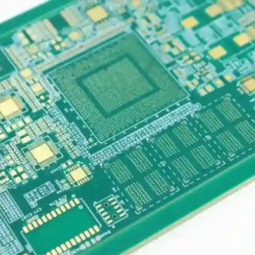
I’ve always found the design process of double-sided PCBs particularly interesting. Many people may not know how many processes are involved behind those little green boards to accurately print complex circuits on both sides.
I remember being quite surprised the first time I encountered photoresist – this stuff is so sensitive to light! The entire operation had to be done in a yellow light room.
Once, when I visited a factory, I saw workers laying out rolls of photoresist on panels and using heat pressing to make it adhere firmly. That level of precision really requires accumulated experience to master.
Actually, I think the most amazing part is the UV exposure step. Watching the circuit patterns slowly solidify under the light, and the excess parts being washed away – this precise control reminds me of making crafts with photosensitive paper when I was a child, only the technology is much more complex now.
I’ve seen some novice designers trying to cut corners, resulting in circuits that are either short-circuited or broken. Double-sided routing requires even more consideration of the coordination between the two layers; sometimes, if a single hole is misaligned, the entire board is ruined.
Now, many electronic devices are getting smaller, and the requirements for PCBs are getting higher. Previously, it was enough if it could conduct electricity; now, we also have to consider heat dissipation and signal interference. Designing a new circuit is like solving a three-dimensional puzzle every time.
However, this challenge makes me even more fascinated – when you see your designed circuit board finally light up the screen or drive a motor, that sense of accomplishment is incredibly real!
I’ve always felt that the most fascinating aspect of circuit board design lies in the invisible details. Take double-sided PCBs, for example; many people only care about whether the circuit layout is reasonable; but what truly determines the product’s lifespan is often the surface treatment, a seemingly minor aspect. I remember a time when we were testing samples, using the same base material; however, the boards without a plating treatment developed oxidation spots in less than two months, while the version with a nickel barrier layer is still working perfectly. This difference made me realize that surface protection is not an option, but a necessity.
The choice of plating is often more complex than imagined. Some people prefer direct gold plating, thinking it’s easier; but in practical applications, direct contact between gold and copper can cause diffusion problems – like forcibly sticking two metals together; over time, delamination is inevitable. Later, we tried adding a nickel layer in between; we found that it not only blocked metal migration but also made the entire structure more stable. Although the cost was higher, it saved us the trouble of later repairs.
Recently, I came across a new process: micro-porous treatment on the plating surface. This method allows the protective layer to adhere more closely to the substrate; it’s like giving the circuit board a breathable raincoat; it prevents oxidation without affecting heat dissipation. Experimental data shows that its corrosion resistance is nearly three times better than traditional processes – this made me rethink the limitations of so-called “mature solutions.”
In fact, many technical bottlenecks are hidden in the details. For example, the via treatment of double-sided PCBs; if the surface roughness is not properly controlled, even the best plating will fail prematurely. Once, I disassembled an old device from ten years ago; I found that its plating was still as bright as new, while some of our current products start to fade after three years – this comparison is worth serious consideration.
Perhaps we should pay more attention to the interaction between materials, rather than looking at each process step in isolation. After all, a truly good design is one where all the details form an organic whole for protection.
I always find circuit board testing quite interesting. When I was working on double-sided PCBs, the most troublesome thing was those densely packed via connections. Once, I spent a long time testing with a multimeter and found no problems, but the board burned out when powered on. Later, I discovered there were tiny cracks inside the vias.
After that incident, I became particularly meticulous about thorough testing. Now, when I see someone just using a multimeter to casually test a few points and think they’re done, I can’t help but say a few extra words. Problems on circuit boards are often hidden in the most inconspicuous places, especially those double-sided PCBs that require simultaneous testing of both sides.
I remember once helping a friend repair an audio device; the impedance of two grounding points was incorrect. The voltage measured normally using standard methods, but problems arose as soon as a load was connected. Later, using four-wire sensing, we discovered that a loose solder joint was causing unstable current. This kind of problem is impossible to detect with just visual inspection or simple continuity testing.
I now prefer combining multiple testing methods. For example, I first perform basic continuity tests and then verify the actual working state with a current load. Some circuits behave normally under no-load conditions but reveal problems once the actual working current flows through them. This is like checking a water pipe; you can’t just see if water flows, you also need to see how it performs under actual water pressure.
Recently, I’ve been experimenting with a dynamic testing method, using high-precision probes to monitor current changes at key nodes while the board is operating. This method can detect intermittent faults, such as poor contact caused by temperature changes. Although it’s more time-consuming, it avoids many later problems.
The essence of testing is to simulate real-world usage scenarios. Circuit boards ultimately need to be powered and operational, so testing must also involve current flow. Static testing only guarantees circuit connectivity; dynamic testing verifies actual performance. This is probably why I always feel that simple continuity testing is just going through the motions.
Every engineer may have their own testing habits, but I think the most important thing is to understand the purpose of testing. It’s not about completing a checklist, but about truly ensuring the board works reliably. Sometimes, spending an extra half hour on careful testing is worth more than days of rework later.
While organizing my workshop recently, I came across some early double-sided PCB samples. Looking at the somewhat crude through-hole designs, I suddenly recalled how my perspective on circuit board manufacturing has changed over the years.
When I first started working with electronics, double-sided PCBs seemed quite mysterious. Once, I tried making a board myself and found that the copper plating in a through-hole wasn’t properly done during the etching process, causing intermittent signals between the layers. This experience made me realize that seemingly simple inter-layer connections require extremely meticulous process control.
Many tutorials now focus on circuit layout, but I’ve found that what truly affects the quality of the finished product are often those inconspicuous details. For example, the treatment of the inner wall of the through-hole; if the copper plating is uneven, it’s prone to cold solder joints. Another example is the choice of board material; ordinary FR4 and high-frequency materials have significant differences in signal integrity.
I remember once helping a friend repair an industrial control board; the cause of the failure was a broken through-hole connection due to prolonged vibration. This incident made me start paying attention to the reliability requirements of PCBs in different application scenarios – consumer electronics might prioritize cost control, while industrial equipment often requires a more robust physical structure.
In fact, after working with hardware for a long time, you gradually realize that good circuit board design requires balancing electrical performance and mechanical characteristics. Sometimes, in the pursuit of perfect impedance matching, the thermal expansion coefficient of the board material is overlooked; or excessive attention is paid to wiring density, leading to difficulties in later maintenance.
Recently, I gained new insights while trying to use a four-layer board for an RF project: the through-hole design of multi-layer boards is much more complex than that of double-sided PCBs. It’s not only necessary to consider electrical connections, but also the impact of vias on signal integrity. These experiences are all accumulated through practical trial and error; textbooks rarely explain these details so specifically.
Looking at the increasingly sophisticated circuit boards today, I appreciate even more those designs that have perfected the basic manufacturing processes. After all, even the most complex design ultimately comes down to fundamental issues like whether each solder pad is secure and whether each via is conductive.
In the field of industrial automation, people often pay attention to AI
Ever wonder how your phone maintains a stable signal? It relies on
When selecting components for a security monitoring system, most attention goes to
- Experte für die Produktion kleiner bis mittlerer Chargen
- Hochpräzise PCB-Fertigung und automatisierte Montage
- Zuverlässiger Partner für OEM/ODM-Elektronikprojekte
Geschäftszeiten: (Mo-Sa) von 9:00 bis 18:30