

Digital X-Ray Detector PCB: Readout Noise, Power Integrity and Production Consistency for Flat Panel Detectors
Flat panel X-ray projects rarely fail at the scintillator or TFT but
A Broadcast Transmitter PCB carries high-power RF, bias and modulator currents, digital predistortion feedback paths and control logic on one board that must run for a decade or more. Linearization algorithms such as DPD and envelope tracking cannot compensate for poor impedance continuity, unstable dielectric constant, weak via filling, inadequate copper thickness or unmanaged heat. Choose high-frequency, HDI and multilayer suppliers by their measured dielectric data, layer registration, via reliability and thermal aging records rather than by price or headline layer counts.
After so many years working on the power amplifier modules of broadcast transmitters, I increasingly feel that what really chokes the throat is often not the linearization algorithms written in textbooks. We spend too much time agonizing over how many parameters to tune for envelope tracking or digital predistortion, and it is easy to neglect the foundation: the board itself. A transmitter’s amplifier board runs at hundreds of megahertz or even above 1GHz, with tens of amps of current flowing on it, and if any single ground via is not handled well, the simulation work done earlier, however beautiful, is wasted. So in recent years I have been especially serious about selecting multilayer board and HDI PCB suppliers, and I will not settle on a multilayer PCB supplier just because the quotation is cheap.
The broadcast industry is different from communication base stations: a transmitter, once switched on, may not be replaced for ten-plus years, and its requirements for long-term thermal stability and high-frequency tolerance of the board material are extremely harsh. I have seen the amplifier board of an old transmitter that used ordinary FR-4 mixed with some so-called high-frequency material. It was fine for the first two years, but after three years dielectric loss rose, VSWR quietly floated upward, and overall machine efficiency fell with it. Can an algorithm compensate for that? No, it cannot. So later, on new projects, I went directly to a high frequency PCB manufacturer to discuss, and it must be the kind of factory that can provide a complete dielectric constant temperature coefficient curve and a copper foil roughness report. HDI also has to go to a reliable HDI PCB supplier, because power amplifier modules are now being compressed smaller and smaller, with final-stage devices of tens or even over a hundred watts crammed onto a board the size of a palm, and if the blind via and microvia processes are a mess, heat dissipation and signal integrity simply cannot both be had.
Another thing many people overlook is the thermal-electrical coupling on a broadcast transmitter PCB. A transmitter amplifier module works for a long time at high temperature and high current, the resistance temperature rise of the traces themselves changes the conductivity of copper, and with the thermal expansion of the board material added, if the vias crack, it is a disaster. My own lesson is that once I find any multilayer PCB manufacturer cutting corners on the process parameters of via filling, I directly reject the whole batch. Because an invisible void could, three years later on some day, make the whole transmitter lose power. In our line, reliability is everything. When a program stops, it is not a matter of compensation; it is an accident.
So now when I chat with peers, I often say: rather than spending all your energy studying a one or two percent improvement in linearity, first stabilize the process level of the board factory. However brilliant a transmitter main amplifier board is designed, if it falls into the hands of an unreliable HDI PCB manufacturer, what comes out is a disaster once you sweep it on a network analyzer. The consistency of dielectric constant of high-frequency material, layer-to-layer alignment accuracy and the effect of surface finish on insertion loss are the foundation for a transmitter to run stably at the edge of the bandwidth without trailing. The hard part of a broadcast transmitter amplifier is not tuning but making it work ten years later as it did on the first day, and the confidence behind that actually comes from the factory you chose to make the board.
I have done several years of maintenance and modification of high-power broadcast transmitters, and I increasingly feel that many designers in this industry have been led astray. Everyone talks about DPD and ET as if you do not deserve to build a transmitter without digital predistortion and envelope tracking. Not long ago I disassembled a prototype sent over by a factory. The routing and copper pours of its amplifier board had a student-homework flavor, and the position of the HDI blind vias drilled into the RF chain was simply outrageous, yet the DPD algorithm derivation in their proposal ran to a full twenty pages. The machine began to lose power after half an hour of warm-up. It was not a question of DPD convergence speed; the thermal expansion coefficient and heat resistance of the high-layer-count board were simply not up to standard locally, and the signal return path had been arched into something completely different from the simulation.
With the PCB of a broadcast transmitter, many times the failure is not insufficient linearization but that the HDI PCB manufacturer you selected did not understand the perverse requirement of an RF power amplifier for layer alignment. I paid for this: last year, on a batch of S-band boards, to save money I switched to a low-priced HDI PCB supplier, and after the batch came back the laser blind via copper wall fracture rate near the power transistor was nearly seven percent. Once you add ET supply modulation, the voltage swing on the board is violent, microcracks widen into opens within a few months, and no amount of DPD adaptation can save it. At that point you discover that finding a true high frequency PCB manufacturer who understands in-plane stress and copper ductility of high-frequency boards is far more practical than adjusting polynomial coefficients all day.
One more point: many people imagine envelope tracking as a miracle device that perfectly improves efficiency, but in practice the loop of the ET modulator is tangled to death with the parasitics of your layout. I have seen a case where the design party used a multilayer PCB manufacturer claiming ultra-high bandwidth to make a six-layer board, but they did not handle the impedance of the amplifier drain supply plane, and the transient current of the ET modulator was cut up by board-level inductance beyond viewing, and the measured efficiency was three points lower than traditional constant supply. Later they switched to a multilayer PCB supplier specializing in high-power RF, remade the stackup, raised copper thickness to four ounces and made the supply network an embedded copper block, and the ET modulation waveform was truly aligned to the saturation point of the amplifier. What does this say? Without a reliable Broadcast Transmitter PCB process as the foundation, complicated DPD and ET cooperation is purely self-entertainment in the laboratory.
I prefer to believe in an iron law: the lifeline of a broadcast transmitter is not the novelty of the algorithm but whether your multilayer board can maintain impedance continuity year after year in a chassis from -30 to 70 degrees. When looking for suppliers, do not look only at whether they carry the name of a multilayer PCB manufacturer; look at whether they have done long-term thermal aging tests with bias current applied. Failure of amplifier bias sequencing is, many times, not a fault of the control circuit but the drift of bias resistors or copper foil resistance after the board is heated, and your debugged DPD memory depth model flies off immediately. Later I made a rule: every broadcast transmitter PCB must designate a high frequency PCB supplier with concrete broadcast power amplifier track record, and every batch must be cross-sectioned to verify dielectric thickness and glass cloth distribution. This money cannot be saved, and absolutely should not be.
At the end of the day, DPD and ET are shadows behind the amplifier. For a shadow not to lose its shape, you must first stand on a board that does not move. Otherwise, however many adaptive algorithms you have, they are only making a strenuous effort to compensate for the congenital deficiency of the physical layer.
When I worked on broadcast transmitters, one thing left a deep impression. DPD: most people put their energy into the algorithm, thinking that if convergence is slow and the model inaccurate, adjusting parameters is enough. When you get to the board, it is a completely different matter. The feedback loop behind the amplifier has to couple from RF output of tens of volts, pass through downconversion, enter the ADC, and then be sent to the processor to compute the inverse model. If the delay of the whole link jitters slightly, the convergence of DPD turns into a total mess. That mess is not because the algorithm is not good enough; the physical link has already put the error in, and no calculation will twist it back. In other words, complexity has not disappeared; it has just moved from code to PCB.
I have found several high-frequency PCB manufacturers to make this board, and basically got stuck in two places: first, impedance continuity in the RF coupling area; second, how to split digital and analog ground in a multilayer board without enlarging the loop area. With the power level of a broadcast transmitter, if grounding is slightly not handled well, the thermal drift of the amplifier immediately turns into feedback noise, and DPD cannot run stably. Later I specially switched to a high Frequency PCB manufacturer who was used to doing this kind of high-power RF board, with their own parameter library for the transition from microstrip to stripline, and who were willing to grind the matching of the coupling section with me, which finally pressed the group delay fluctuation of the feedback to within one sampling period. In the middle I also tried a multilayer board supplier claiming to make high-end RF, but the layer alignment deviation directly made the differential pair impedance jump, and DPD convergence time dragged from 0.5 seconds to nearly 3 seconds, and startup compliance simply could not be met.
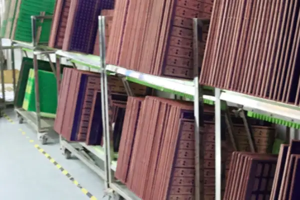
Speaking of the board structure itself, many people think a broadcast transmitter can use an ordinary multilayer board, and I completely disagree. For a scene mixing amplifier plus DPD feedback, high voltage, high frequency and mixed signals, the advantage of HDI is not the precision; it is that you can bury the BGA fan-out traces of the feedback ADC directly in the inner layers, drilling two fewer through holes, which is critical for reducing loop inductance. Later I had an HDI PCB supplier prototype a fourth-order stack, putting even the memory bus of the digital predistortion processor into the build-up layers, and the overall noise floor dropped a bit more, and the adjacent channel leakage ratio of DPD stabilized by nearly two dB. An algorithm simply cannot save this.
DPD for broadcast transmitters particularly depends on the memory effect model of the amplifier. Base station bandwidth is wide but power changes fast, so the memory effect is not as prominent; broadcast channels are narrow, but a transmitter, once on, runs for more than ten hours without rest, and after the junction temperature of the amplifier tube climbs, the tail dragged by thermal memory is very long. At this point the order of the inverse model cannot be simply cut, and once cut, EVM takes off. A high model order means large data throughput between the processor and the feedback channel, and the high-speed serial link on the PCB cannot have any stubs. I paid for this: a board from a multilayer PCB manufacturer came back and the differential via stub length on the inner layer formed a resonance exactly at the 6GHz harmonic, the feedback data eye closed by a third, and DPD lost lock directly. Finally I changed to a multilayer PCB supplier with a revised blind-buried via scheme, ground off the stubs, and the link was opened.
So now when someone talks to me about DPD for broadcast transmitters, about algorithm complexity and model simplification, I usually ask just one sentence: can the few pieces of copper on your feedback link withstand RF leakage above 50 watts without crosstalking into the digital area? If so, we can talk about other things. If not, however many effective bits there are, it is all wasted. Choosing the right HDI PCB manufacturer and a high-frequency PCB supplier that truly understands mixed high-voltage high-frequency signals is, in time, much faster for the linearization implementation of the whole system than scratching at that bit of complexity in the algorithm. I think this is the lifeline of broadcast transmitter hardware and the most underestimated place.
Not long ago there was a project that made me rethink DPD again. The Broadcast Transmitter PCB we made kept grinding on algorithms at first, always feeling that as long as the mathematical model was beautiful enough, distortion could be suppressed. Later, after several board revisions, we found that what truly dragged us down was not code but the board itself. Especially the feedback channel: if you casually find an HDI PCB manufacturer with an ordinary process, solder mask thickness deviation or slightly off layer alignment makes the phase of the whole feedback link simply fail to line up, and then the predistortion coefficients computed by DPD are basically self-deception.
At the time I directly threw the design to a high Frequency PCB manufacturer who specializes in high frequency, who did very careful impedance control on the stackup and also deliberately kept the feedback traces far from the amplifier output. But one point is easily ignored: if the multilayer PCB supplier you use cannot guarantee the batch stability of the dielectric constant of the board material, then your DPD training applies only to this one board, and changing to another board means re-converging. I paid for this: in one batch, two boards came from different multilayer PCB manufacturers, and the group delay measured on the RF link differed by tens of picoseconds, and the phase of the returned feedback signal turned a few extra turns, causing the DPD model to compensate blindly in the low and high bands.
Later we simply separated the feedback channel and used a small four-layer high-frequency board snapped onto the main board through a connector, specially made by an HDI PCB supplier that supplies radar. It was expensive, but what the feedback ADC captured was finally clean. I think that now everyone likes to talk about filter bandwidth and polynomial order when discussing DPD, which are of course important, but if you cannot even build a stable, low-noise feedback path, distortion simply cannot be cured. A broadcast-band transmitter works with a slight swing in load VSWR, the nonlinearity of the amplifier is changing, and if the feedback link drags in even a little spurious, the whole adaptive process becomes finding signal in noise, which is worse than turning off DPD and honestly reducing power.
So now when someone asks me where to start with transmitter predistortion, I actually do not recommend reading papers first. First swap your cooperating multilayer PCB supplier for one that truly understands RF, see whether they can use low-profile copper foil for the layers of the feedback traces, and then confirm with the high Frequency PCB supplier the effect of glass cloth weave on differential phase shift. If this foundation is not laid, however fancy the DPD algorithm, it cannot save your linearity.
I still remember that project to this day: a UHF broadcast transmitter whose amplifier board was revised four times, nearly delaying delivery to ruin. Where was the problem? Not the schematic, not device selection, but that the multilayer board supplier found first had never made high-power RF things. Their engineers were quite enthusiastic, but when it came to the dozens of amps of current traces on the Broadcast Transmitter PCB, with copper thickness to be 3 ounces and temperature rise to be controlled, they could only apply ordinary digital board thinking. When the prototype came back and was measured, the microstrip line impedance at the PA output wandered out of shape, VSWR went high, the amplifier’s efficiency dropped directly, let alone linearization.
Later, through a peer’s introduction, I changed to a high-frequency PCB manufacturer truly rooted in the RF circle, and things improved. Their people came to look at our stackup requirements and opened by asking how long we planned to run the offset line of the Doherty combiner and how much copper foil roughness we could accept, and also suggested changing the key matching sections to a blind and buried via structure to reduce parasitics. Only then did I realize that the HDI PCB suppliers in this business and ordinary multilayer board factories have two completely different coordinate systems in their heads. It is not a matter of machine accuracy but of engineering experience: he has to understand the heat distribution of your amplifier, understand how dielectric constant drifts with temperature, and even care more than you about those few dB of insertion loss.
I felt it even more deeply with DPD. When we built the predistortion chain with an FPGA, we always wanted to push the order of the memory polynomial higher and set the memory depth larger, feeling that the more complex the model, the better the compensation. After burning it in and running, timing simply would not converge, DSP slices were eaten by more than half, the update rate could only reach a few dozen Hz, and we could not even catch the tail of thermal memory. When I talked with the engineer at that high-frequency PCB supplier, he asked me: the copper traces on your board have little electrical memory themselves, so why do you need such a deep memory depth? It would be better to lower the order and use the saved resources to raise the update rate; thermal memory relies much more on faster tracking than on more taps. After I readjusted along this line, the shoulders of the amplifier’s output spectrum really did pull back.
Looking back now, whether choosing an HDI PCB manufacturer or tuning a DPD model, it all comes down to balance. You cannot expect an algorithm to repair all distortion on a board with large transmission line loss and uncontrollable coupling spurs. Honestly making the physical characteristics of the board solid, letting the amplifier sit in a relatively clean operating window, and leaving the remaining bit of nonlinearity to DPD is actually the most labor-saving path. Do not superstitiously trust high-order models, and do not lightly trust that every multilayer PCB supplier dares to take a broadcast amplifier job; if the board’s foundation is weak, anything piled on it will shake.
In these years of working on RF power amplifiers, what gave me the most headaches was not the circuit itself but how to make the combiner on the PCB. At first I also thought it was convenient to integrate the combiner and the power transistor on the same board, with short routing and well-controllable parasitics, but only after the stone dropped on my own foot did I understand: once the band changes, the whole board has to be redone. Especially in a project like a broadcast transmitter, a Broadcast Transmitter PCB often has a dozen or so layers, and cost is no small matter. Later I simply pulled the combiner out and made it a separate small board, and when changing bands only that small board is discarded, and the pressure in my heart eased a lot.
But it was not that simple. The small board and the main board have to pass through an RF connector, and once high power is applied, if insertion loss is slightly larger, the load-pull behavior goes crooked outrageously. I remember one efficiency measurement that was off by seven or eight points no matter what, and three days of checking revealed that the SMA connector heated up under high current and its contact resistance drifted. That lesson made me fully recognize that for this kind of board, looking for a multilayer board supplier and an HDI board supplier follow completely different logic. Do not get a headache hearing multilayer and think more layers is better; the key is how you allocate ground layers and power traces. The high-current path on a Broadcast Transmitter PCB must be short, straight and wide, and at this time the conventional stackup experience of multilayer board manufacturers is often not enough; you must calculate copper thickness and temperature rise yourself, and arguing with them is common.
For a while I wanted to save trouble, searched online for a bunch of multilayer PCB manufacturers, and deliberately marked that they must be able to make high frequency. As a result, the prototypes came back and I found the substrate they used was not the high-Tg low-loss material I wanted at all. After asking I learned that many multilayer PCB suppliers by default give you ordinary FR-4 unless you note the board model on every work order and watch it closely. Later I learned and directly went to a high Frequency PCB manufacturer specializing in RF, who stocked Rogers or similar ceramic-filled material and had much smaller temperature drift. Combiner routing is too sensitive to dielectric constant, and when temperature goes up and phase shifts a bit, load modulation in a Doherty amplifier is messed up and efficiency falls faster than a stock. A pit like this is enough to step into once.
Interestingly, later I came into contact with some compact solutions where customers forced the size to be small, and I also tried finding an HDI PCB supplier to use microblind vias to bury the combiner in the inner layers to save area. But the HDI process has via current-carrying problems for high-power RF, and ordinary HDI PCB manufacturers are used to making digital boards and have no concept of continuous-wave RF current of tens or hundreds of watts; if the via wall is a bit thinner, it burns out instantly without negotiation. So now, unless the power is small, I would rather let the combiner use sturdy independent traces than chase high density. For a power amplifier, what is valued is ruggedness, especially on a broadcast transmission occasion, where stability beats everything. For the board of the combiner now, I try to specify a high Frequency PCB supplier using low-Dk-drift material, and even if it is more expensive, every time I finish testing and look at the steady efficiency curve, I feel it was worth it.
Previously I always thought RF power amplifier work meant just tuning the match and choosing the transistor, and only after taking over the broadcast transmitter job did I find that what truly keeps one awake is the pull between modulator and PCB. At that time we wanted to use ET to raise efficiency in the amplifier back-off region. The principle was clear: let the drain voltage follow the envelope so that the transistor wanders near saturation. But once made into physical hardware, it is all pits.
The modulator itself is a wideband amplifier that must chase signal envelope changes, and as bandwidth goes up, switching loss and linearity fight each other. I tried pushing the tracking bandwidth above 20MHz, and the result was painful efficiency loss, while the transistor’s heat rose steadily. Later I figured out that the problem was not on the modulator chip but that the board underneath simply could not support this rhythm. The size of a Broadcast Transmitter PCB is generally large, and if the ground plane is not slightly tidy, the large-current path at the modulator output becomes an antenna, smearing noise onto the RF chain. I had the engineer do the drain feed of the supply modulator on the third layer of the multilayer board, using the whole layer as a power island with a whole copper sheet underneath as ground, with vias drilled directly onto the GND copper, with no island-ring fake grounding. This trick I learned from a master who worked at a multilayer PCB supplier; they supplied base station boards for a long time and had their own rule-of-thumb methods for return control of power circuits.
After the grounding hurdle was passed, the bottleneck of efficiency ran to the stackup. To withstand the current slew rate at the moment the modulator switches, we needed an extremely low-inductance path, which meant finding an HDI PCB manufacturer who could make extremely small via diameters, and also had them plug the holes, since without plugging, wave solder flooding in would collapse the impedance into a mess. A good half of the factories nominally able to make high-frequency boards stammered when they heard plugged hole diameter of 0.15 millimeters, and after several rounds of trying I settled on one HDI PCB supplier willing to fiddle. They truly understood the effect of parasitics on that section of high-speed modulation signal vias, not just talking about aperture. In measurement, the inductance of the feed loop from modulator to amplifier transistor could be pressed below 0.3nH, and running a 16MHz LTE signal, efficiency could still hang near 58%. Although it still got hot, at least it did not fall out of the margin we left for the system.
This matter circled back to a particularly plain feeling: for high-frequency power amplifiers, especially dynamic supply things like ET, the so-called design freedom depends entirely on what kind of multilayer PCB manufacturer you can find. The lamination structure and dielectric thickness of ordinary industrial control boards, under the envelope components of the modulator at hundreds of kilohertz to a few megahertz, have loss that eats up your bit of efficiency optimization in a blink. It still takes a true high Frequency PCB manufacturer who runs high frequency and is familiar with the RF resin system to make hybrid stackups steady; otherwise once temperature drift arrives, the modulator linearity is hopeless. I remember one night tuning a board, I changed samples from three suppliers, and the one that finally worked came from a high Frequency PCB supplier that does no advertising. They used hydrocarbon-ceramic mixed dielectric, with very small Dk change over a wide temperature range, and the AM distortion of the supply modulator finally stopped drifting upward as the chassis warmed.
So now when someone talks to me about ET amplifiers, my first sentence is to ask who made the board. The pair of enemies, modulator bandwidth and efficiency, with no reliable multilayer structure and via process to carry it, even the best circuit simulation is only noisy on paper.
After working on several high-power broadcast transmitter projects, I developed a certain obsession about the PCB layout of the supply modulator. Many people isolate, split and surround with ground by the book, and those textbook practices indeed suppress differential-mode interference to a good extent. But what keeps people awake at night is the common-mode current running wild across the whole board. Once, on an eight-layer board of ours, the switching node of the amplifier supply modulator was less than two centimeters from the RF output balun, theoretically isolated, with the ground plane slotted too, but after power-up, spurs near the antenna port could not be eliminated no matter what. Only after putting the board up in the air did I find that the switching noise was not coupled over by traces at all: the whole heat sink had acted as a flat plate capacitor, pushing dv/dt directly onto the chassis ground and then forming a huge loop antenna through the outer skin of the coaxial cable. So now, when I make this kind of Broadcast Transmitter PCB, the first thing I watch is not trace spacing but the ground loop of structural parts and the distribution of mounting hole positions. This kind of thing is seldom written in materials, but once you suffer enough, you naturally remember.
Speaking of board layers, if the envelope path and RF main path in an ET system are to be truly time-aligned, relying merely on delay lines to patch it will drift as soon as temperature changes slightly. I prefer to put compensation into the digital domain, but this in turn requires the baseband processor and DAC to be close enough to the modulator so that trace delay is controllable. The board will then be crammed with a heap of high-speed differential pairs and RF microstrip lines, and traditional multilayer board practice is no longer quite enough; instead, the demand for the HDI process suddenly appears. A reliable HDI PCB manufacturer will directly decide whether your blind and buried vias can control the parasitic inductance of the envelope detection channel within a reasonable range, otherwise the edge of the detected envelope signal itself has collapsed by half, and what precision is there to talk about. I once changed to an HDI PCB supplier who did not care much about stackup symmetry, and the board that came out warped directly after hot-air reflow, and the impedance of the amplifier supply loop was two orders of magnitude higher.
On multilayer boards, I do not superstitiously believe that more layers advertised by a manufacturer is better. What four layers can solve, if forced into six layers, only makes interlayer coupling more complex. But in a mixed-signal plus RF system, a multilayer PCB manufacturer who knows how to control dielectric thickness tolerance does save worry. For example, the supply copper thickness needed by the amplifier final stage and the narrow line width required by RF signals often fight each other, and they can give a reasonable local plating scheme instead of a one-size-fits-all cut. And if the switching frequency of your modulator is pushed relatively high, the additional loss from copper foil roughness must be negotiated at the material selection stage, a detail directly tied to the engineering capability of the multilayer PCB supplier.
High-frequency material is even more so. Now some signal modulation schemes push the update rate of envelope mapping to over a hundred megahertz, and the delay difference between the corresponding envelope detection and amplifier input must be less than the nanosecond level. At this point, even if the dielectric constant of ordinary FR-4 is marked beautifully, once the glass fiber effect arrives, the differential phase changes every time. So I would rather spend more budget on a high Frequency PCB manufacturer specializing in RF, who at least knows how to handle the directionality of glass cloth and how to avoid passive intermodulation hazards at certain copper foil bonding surfaces. A qualified high Frequency PCB supplier should be able to provide impedance strips with stackup electromagnetic simulation support before production, rather than just throwing you a standard lamination table. Do not underestimate this step: a via stub that looks unremarkable on the envelope path can make the edges of a wideband modulated signal ring, and the ringing is transmitted through the amplifier’s instantaneous supply to the RF output, indirectly pulling down ACPR, and in the end no matter how you look, you cannot find it at the power source.
Over these years I have felt more and more that the cooperative design of RF and envelope is, rather than a circuit problem, a comprehensive problem of space allocation and material selection. Imagine the return path under the decoupling network of the amplifier supply as a three-dimensional structure rather than a single-layer plane current direction, and many so-called interference leaks can find their real root. Many times, when you get the board, without even powering it up, just looking at the burrs at the copper edge and the flatness of resin-filled holes, you roughly have a clue. What a good board factory makes has clean microstrip edges under the solder mask, which says more than any parameter in a brochure.
After so many years working on high-power broadcast transmitters, I increasingly feel that the cooperation of board selection and circuit architecture is far more important than the formulas in textbooks. When I first entered the line, I always thought that as long as the transmit chain was calculated accurately and the output match was well tuned, there would be no big problem, and only after falling a few times did I understand that the process from drawing to physical object of a Broadcast Transmitter PCB basically determines the failure rate of this machine in the coming years.
The project that left the deepest impression on me used a GaN transistor that was quite popular at the time, with high efficiency and decent linearity. The first prototype ran quite happily, but after it was sent to the customer site, in less than two months the amplifier started to intermittently lose power. After checking around, the problem was not in the transistor itself but in the DPD feedback link. The routing on that multilayer board had not been given strict length-matching constraints, and the path difference between the envelope signal and the baseband signal entering the DPD processor was nearly one hundred and twenty picoseconds. At room temperature this deviation could be calibrated back barely, but once the temperature inside the chassis exceeded forty-five degrees, the PA’s AM-AM and AM-PM curves drifted, and DPD started to compensate wildly, instead raising adjacent channel leakage. Since then I have paid special attention to finding a reliable multilayer PCB manufacturer, not merely drawing a stackup and throwing it over. I need the other side to understand the timing relationship between RF sampling lines and high-speed digital lines, to help me control the delay of those key differential pair groups, instead of simply processing according to production files.
Choosing a board factory later slowly became a screening process. Some factories calling themselves HDI PCB manufacturers actually only dare to take small boards of consumer type, like phones or tablets, and when they hear that you want to make a large-size, thick copper, hybrid-laminated high-frequency broadcast board, they stammer and begin to talk about extra charges. The multilayer PCB supplier I later settled on for long-term cooperation had RF background in their own engineering, and would proactively remind me that laser blind vias may have stress problems under repeated thermal cycling, or suggest the practical benefit of a certain hybrid stackup for lowering transmission line loss. The communication efficiency of this is too high, nothing like a processing-agency mode where you send files and he just does it. Especially when buried capacitance, stepped slots or local thick copper are needed, a knowledgeable HDI PCB supplier can save you several rounds of revision time.
I am more cautious on the high-frequency board side. The output network of the final stage and the combiner section of a broadcast transmitter have extremely tricky requirements for dielectric loss and thermal stability. For a period hydrocarbon ceramic boards were short in the market, and I tried replacing material from another high Frequency PCB manufacturer. The nominal dielectric constant looked quite close, but in the high-temperature VSWR test the phase drift differed by nearly double, so the VSWR protection threshold had to be revised repeatedly in the whole machine test. Later I changed to another high Frequency PCB supplier willing to provide measured Dk data per batch, and only then was this block stabilized. My experience is that the nominal parameters of high-frequency material are just a door knocker; a truly reliable design must be built on the foundation that the supplier is willing to provide measured impedance strips and batch consistency data, otherwise volume production consistency cannot be guaranteed at all.
Back to the old enemies VSWR and junction temperature. Many manufacturers claim their amplifiers can withstand VSWR 3:1 without burning the transistor, but that is measured only under laboratory pulse conditions. High VSWR at a real site caused by icing on the antenna-feed system, interface oxidation or feeder deformation is often a chronic deterioration process. I found that when VSWR slowly climbs close to 1.5, the reflected power pushes up the PA’s junction temperature, junction temperature rise makes the output impedance drift, which further aggravates mismatch. This is totally a positive-feedback pit, and once you fall in, the amplifier transistor lasts half a year at most. So in the past few years, in layout, I deliberately place the VSWR detection circuit after the circulator at the position closest to the antenna port, and use an independent ADC to sample forward and reverse power, ensuring that the response time of VSWR protection is shorter than the inertia of rapid junction temperature change. At the same time, the copper area under the amplifier transistor on the PCB is filled with vias directly through to the metal base plate on the back, to pull down the thermal resistance on the Rth(j-c) path as far as possible. Many times a burnt transistor does not mean the transistor’s own limit is low, but that when we designed the PCB we did not leave the heat a sufficiently low-resistance path.
Some peers like to treat DPD as a cure-all, thinking nonlinearity can be pushed away entirely by algorithms. I gradually understood that the range DPD can compensate is actually rather limited, especially when memory effects are involved. If your front-stage power decoupling is not done well, or the IR drop point of the PA supply routing is too close to the final stage, then the dynamic bias modulation caused by envelope changes makes the DPD model fail completely within a few symbol periods.
When I first came into contact with broadcast transmitters, someone always made the junction temperature of amplifier transistors mysterious, as if you must use an infrared thermal imager to understand. In fact, the most easily neglected place is often the thermal resistance of the copper layers and via arrays on the multilayer PCB itself. The power loop traces of a Broadcast Transmitter PCB are dozens of amps, and if the multilayer board supplier did not fully consider copper thickness and dielectric thickness when designing the stackup, even if the high-frequency PCB manufacturer you chose is the best, the board will still burn your hand once running. I have seen a case where the board was originally made by an ordinary multilayer PCB manufacturer whose vias were not resin-plugged, and during SMT solder flowed directly into the holes, causing large voids on the soldered surface between the flange and PCB. The result was that junction temperature was 15 degrees higher than expected, and power derating was severe.
Later I changed to a professional HDI PCB supplier, and things were completely different. It was not because they used any rare material but because in the high-density interconnect structure they handled the heat dissipation details very well. For example, laser blind vias were drilled directly under the pad and connected to a large area of copper in the inner layer, and thermal resistance came down at once. You find the junction temperature curve becomes smooth, and once the DC bias is applied, though the device case still feels hot to the touch, the heat inside the chip spreads quickly. The protection circuit also does not need to be so nervous; there is no need to set the reflected-power threshold excessively conservatively, because the board’s own heat dissipation capability gives design margin.
Another very realistic issue is bias sequencing. When I debugged boards, I found that in the reference designs provided by some high frequency PCB suppliers, the delay between gate bias and drain power-up is often insufficient. The parasitic inductance and capacitance of board-level traces make the time it actually takes to establish stable bias slightly longer than simulation. That slight bit on a GaN amplifier is fatal: once the drain surges up before the gate has settled, the instantaneous large current is enough to burn the transistor. Thinking back, many reliability problems are not that the device itself is bad but that the parasitic parameters of the multilayer PCB were not taken seriously at the layout stage. A good HDI PCB manufacturer knows how to shorten bias traces as much as possible and use inner layers for shielding to avoid crosstalk. This is the idea of fundamentally lowering thermal resistance and protecting junction temperature.
Years ago, when I made the amplifier module of a broadcast transmitter with a multilayer board supplier, I fell. At that time, to save trouble, I found an ordinary multilayer pcb manufacturer without RF background, and the bias circuit kept making trouble. The gate bias voltage of the amplifier transistor drifted often, and after checking everything, it was not a reference source problem: the bias trace and the switching power supply path had coupled in an intermediate layer. Their factory’s layer structure was unfriendly to RF, and ground return impedance was large, so as temperature went up the voltage drop changed with it. Later I changed to a high frequency pcb manufacturer specializing in high frequency, who redid the stackup directly according to RF amplifier habits and placed the bias decoupling right against the transistor pin, and the problem finally quieted down. So now when I look for an HDI PCB supplier, I first ask whether they have done boards related to transmitters, otherwise the communication cost is too high.
The pit on the cavity is more hidden. Everyone knows a metal cavity itself forms resonance, but many people think that making the cavity smaller solves everything. In fact, if the cavity size happens to be stuck on a higher-order mode of the working band, then even if it is made smaller, the resonant energy can still couple to the amplification chain through slots. I met a whole machine whose efficiency dropped inexplicably at a certain frequency point, but tested separately after dismantling the module it was normal. Later I found that the cavity resonant frequency fell exactly within our signal bandwidth, and the load impedance was pulled off at the resonance point. Merely pasting absorbing material only suppresses surface current; the root is still the boundary condition of the cavity and the ground plane of the PCB. If the HDI PCB manufacturer you find can make an electromagnetic band gap structure directly into the inner layers, suppressing surface waves in key areas, the fault tolerance of cavity design is much higher.
At the end of the day, a broadcast transmitter PCB is not a simple circuit board; the stability of the bias network and the electromagnetic environment of the cavity are two sides of one coin. Choosing the right multilayer PCB supplier saves too much trouble of debugging later. Especially for multi-stage Doherty architectures, the bias of the main amplifier and the peaking amplifier must be adjusted independently, which places high demands on the impedance control capability and consistency of the board factory. I now lean toward cooperating with teams who have both high frequency pcb supplier capability and experience in cooperative design of amplifier cavities, so that problems do not all get thrown to the back-end debugging stage, where that kind of repeated fiddling truly cannot be afforded.
After contact with several broadcast transmitter projects, I gradually realized that everyone often over-focuses on link budgets and waveform design but rarely discusses the selection logic of the PCB itself. A Broadcast Transmitter PCB is two different things from an ordinary digital board: high-power RF routing and digital control are mixed together, and the board material and processing determine the stability of the whole machine for long working hours. Once I encountered a very interesting phenomenon: the noise floor of the DPD feedback channel got very bad once ambient temperature came up, and it took a long time to investigate before finding it was not an algorithm problem but that the interlayer dielectric of the PCB had microscopically disturbed impedance continuity after thermal expansion. Put plainly, however strong your back-end correction algorithm is, as long as the raw signal-to-noise ratio of the high-frequency feedback path cannot go up, the real-world effect of DPD will certainly be discounted.
Many people are used to treating the combiner as an independent functional block, finding any multilayer pcb supplier to make the board, soldering it on and calling it done, but this approach is especially unreliable in the broadcast band from 85MHz to 108MHz. The copper pour loss and spurious modes in the combiner region need to be controlled through physical parameters such as stackup thickness and copper foil roughness, which cannot be calculated clearly only through circuit simulation. I personally prefer to choose a high frequency pcb manufacturer with long-term processing experience on RF boards, because they have more stable production line capability in copper stripping accuracy and dielectric thickness uniformity, which is much more important than the nominal dielectric constant on paper. Sometimes, changing to another multilayer pcb manufacturer, with the same schematic, the impedance Smith chart of the combiner port can be off by a large distance, and this is the real influence brought by process differences.
In addition, I am quite averse to focusing only on the old through-hole process way of thinking, especially as the digital part of a transmitter becomes denser. The digital predistortion control module and monitoring sampling paths are now crammed onto the same board, with high routing density needing impedance isolation, and at this point the blind and buried via scheme provided by an HDI pcb supplier is much more comfortable. HDI lets you split ground and power layers more freely, which directly helps reduce crosstalk between the digital part of DPD and the RF power part. Before, with conventional multilayer boards, we had to sacrifice a lot of isolation distance in routing and finally patch it with a metal shield, but later verification found that the resonance points of the cavity were changed instead. After switching to the HDI process, although the single-board price went up a bit, the troubles on the cavity could be dissolved ahead of time inside the PCB stackup.
So now, when I contact a new hdi pcb manufacturer or high frequency pcb supplier, I generally first see whether they are willing to disclose actual processing tolerances and impedance control deviation records, instead of looking at how many lines of industry jargon they can recite. A reliable manufacturer will admit the dielectric thickness fluctuation of high-frequency boards during lamination and tell you how they compensate for a specific copper thickness. The matching network of the combiner and amplifier stages is extremely sensitive to line width etching precision, and a broadcast tower feeder system a hundred meters long cannot tolerate accumulated deviation of a dozen ohms. The PCB in your hand is not an ordinary circuit substrate; it is itself part of the transmitter’s linearity and efficiency. Detached from this perspective, talking about DPD’s adjacent channel power ratio improvement is somewhat putting the cart before the horse.
Some time ago I refurbished an old broadcast transmitter, and the problem was on its core Broadcast Transmitter PCB. After taking the board out, even the grounding copper at the edge was slightly curled, and there were obvious oxidation marks at the press-fit position of the cavity partition. Many people encountering this kind of fault think first of aging of the amplifier tubes or drift of the bias circuit, but what is truly tricky is often the cooperation between the PCB itself and the cavity structure. That board was an early ordinary multilayer board with sparse grounding vias, and the cavity resonance point was nearly two hundred megahertz off the design value, and when reflected power was large the protection circuit simply had no time to act.
This made me ponder one thing again: when making this kind of RF amplifier unit, choosing the right multilayer pcb manufacturer is more important than stacking materials. In the past I was used to squeezing the high-speed digital part and RF chain onto the same board and then finding a cheap multilayer pcb supplier for low-price prototyping, and after several times I found that even with exactly the same stackup, boards made by different manufacturers had completely different spurious responses at the bias feed port. If resin flow around signal vias is not well controlled, the phase stability of the high-frequency feedback channel is totally finished. Now I give the routing of the modulation feedback loop separately to an hdi pcb supplier familiar with RF, and even if the unit price is higher, at least when they tune laser drilling parameters they know what they are doing, and the spacing from blind vias to inner copper will not be arbitrary.
Many people think the cavity is only an electromagnetic shielding shell, and that after drawing the circuit you just stuff it in and are done, a thought that kills. In one all-solid-state transmitter upgrade project I observed an interesting phenomenon: just moving the placement of the decoupling capacitor of the bias network on the PCB by less than three millimeters changed the mode spectrum inside the cavity. Later I found a high Frequency PCB manufacturer to remake the board, specially widened the grounding copper foil at the partition press-fit area, and extended whole-sheet copper in the inner layer, and only then did the cavity resonance mode return to the simulated range. This made me thoroughly realize that when making high-frequency, high-power things, PCB design and cavity machining must be synchronized, especially when the high Frequency PCB supplier you use has its own set of habits for surface treatment processes, the batch consistency becomes particularly delicate.
Speaking of bias, there is another pit worth recording. The gate bias sequencing of a transmitter final-stage amplifier cannot be guaranteed foolproof just by software delay. I once met a strange fault where, in a certain batch, an hdi pcb manufacturer shrank a solder mask opening at an inner-layer buried hole by less than 0.05 millimeters during processing, causing the RC charge-discharge time constant of the bias feed network to drift out of the expected range at low temperature. The digital controller had clearly pulled the IO port and the drain voltage was applied in sequence, but the gate drive voltage was just several milliseconds late, and in that short window of emptiness, the amplifier transistor withstood the surge reflected back and broke down on the spot. Later I required that every PCB spot-check its timing waveform on entry, put the rising edges of gate and drain on the same screen, and never again dared to trust only the typical values on the datasheet.
After making this kind of board for a long time, I have a stronger obsession with the technical accumulation of multilayer pcb manufacturers. For example, impedance continuity on the RF chain cannot be solved by simple line width compensation; copper foil roughness and dielectric thickness batch deviation roll into real phase errors above 900MHz. So now I first look through the supplier’s own capability verification reports to see whether they have DK/DF tracking data for high-frequency board material, instead of comparing only price. A Broadcast Transmitter PCB made bumpy cannot be saved even by being put into the prettiest cavity; whether power cannot be pushed up, or it is pushed up but the spectrum scatters into a mess, in the end all come down to two words: process control.
In these years working on the RF chain of broadcast transmitters, what gave me the biggest headaches was not the choice of amplifier transistors, nor the digital predistortion algorithm, but that PCB which looks like anybody could make it but where a bit of error makes the whole machine’s efficiency fall. Many people think that RF boards just need a high frequency PCB manufacturer to prototype, but it is really not that simple. I have changed five multilayer board suppliers before. Even for the same six-layer board, some came back and after running for an hour on power began to show gain drift like a smile curve, and the insertion loss in the combiner region was nearly 0.3 decibels larger than the simulation model. Those 0.3 decibels, on an 800 watt whole machine, directly eat several percentage points of final-stage efficiency, and heat loss appears out of thin air, requiring higher fan speed, changes to the chassis air duct, and chain reactions.
So my habit now is not to talk to any multilayer pcb supplier about the board can be made; rather I bring up three points right away. First, the combiner section of a broadcast transmitter must use the high-Tg low-temperature-drift board material I specify, with no substitution accepted. Second, ground vias should not be sparse big holes; they must be small diameter, plugged and electroplated flat, to guarantee impedance continuity at several GHz. Third, do not randomly open the solder mask in all RF routing areas, and the copper thickness of the antenna matching section must withstand long-term thermal cycling. Only if these three points are met will we continue discussing the process. Among them, many factories bill themselves as hdi pcb suppliers, but ask how microvia filling is done, and they are vague, and you know they have been making consumer electronics and never touched continuous high-power RF environments.
The difference between Broadcast Transmitter PCB and an ordinary communication base station board, I think, is that two dimensions, sustained thermal stress and peak envelope, are pulled to the extreme. A base station can catch its breath by relying on TDD duty cycle, but a broadcast transmitter, once on, runs for over ten hours, and the RF current density on the PCB of the final-stage combiner and filter section is extremely high. If the copper foil surface has even a little uneven roughness, conductor loss can drop efficiency a notch, and efficiency dropping a notch means the whole machine’s heat loss rises a notch, the internal chassis temperature in turn pushes up the dielectric constant drift of the board material, and efficiency falls further. This death spiral I have seen with my own eyes on two prototypes. So when I choose a multilayer pcb manufacturer now, I particularly care whether the supply chain for their high-Tg material is stable, and I even require them to run small-batch temperature cycling tests on a vector network analyzer first, confirming that the temperature drift curve is within what I can accept before releasing the batch.
Another easily overlooked point is thermal isolation in layout. I physically separate the switching-stage PCB of the modulation supply, the digital control board and the RF amplifier-stage PCB, and have them made by different manufacturers each good at its own. The digital board is fine with HDI, and any mature hdi pcb manufacturer can do first or even second order, with cost also reducible; but the final-stage RF board must be made by a high frequency PCB manufacturer who knows the business, with etching accuracy and undercut control of the routing watched closely. I have seen teams who, to save trouble, had one factory do everything, and the result was that the supplier compromised the process: RF loss was large and the digital board was ridiculously expensive, pleasing neither end.
I also want to say two words on the protection circuit: do not superstitiously trust the speed of software protection. Several times in the debugging phase I met VSWR alarms flashing at the antenna port, and before software could execute the power-reduction procedure, the final-stage amplifier transistor had already burned. The reason was that the link delay from reflected power through the coupler to the detector to the ADC is tens of microseconds, and in those tens of microseconds, under a high peak-to-average signal, GaN junction temperature can overshoot. Later my approach was to add, at the PCB level, an independent analog comparator circuit for reflected power, built with a power divider and Schottky detector, with the comparator output directly pulling down the gate bias, physically completing shutdown within 1 microsecond without waiting for software. The routing of this analog protection loop must be treated as an RF signal, and the slightest extra length makes it oscillate. During debugging I looked at it edge by edge on an oscilloscope before stabilizing the feedback path.
Looking back, the design of the RF power core of a broadcast transmitter is long since not an isolated RF circuit problem; it is the coupling of RF, heat and power electronics on the physical carrier of the PCB. Efficiency improvement cannot be achieved by staring only at the PAE curve of the amplifier transistor; the choice of board material, the return path planning of the multilayer board grounding, the electromagnetic sealing at the high-frequency connector area, and even the residual copper rate of the via plugging process are all quietly eating your system efficiency.
Flat panel X-ray projects rarely fail at the scintillator or TFT but
Fan walls that mysteriously lose RPM are often a board problem, not
Working on battery formation equipment, I learned that test accuracy depends not
- Experte für die Produktion kleiner bis mittlerer Chargen
- Hochpräzise PCB-Fertigung und automatisierte Montage
- Zuverlässiger Partner für OEM/ODM-Elektronikprojekte
Geschäftszeiten: (Mo-Sa) von 9:00 bis 18:30
Get quote, solution or any question, Andre always here to help