

Distributed Antenna System PCB Design: PIM, Multiband Isolation and High-Frequency Laminate Selection for In-Building Coverage
Anyone in RF knows the Distributed Antenna System PCB in an in-building
My first contact with vehicle-grid interaction was purely accidental. A friend who was doing a retrofit of charging facilities for an old residential community dragged me in to look at a bidirectional OBC board. At that time I still thought it was just running the charging loop in reverse, and that a software adjustment would be enough. Later, when I actually drew my first version of a V2G PCB, thinking back to what I believed at the time, it was honestly a bit laughable.
I still remember why that board was scrapped: it was not that the logic did not work, but that the heat from the top-layer devices ran straight down the copper foil, and the inner power layers of the four-layer board simply could not withstand long reverse inversion. Especially in a residential backup power scenario, with the car parked in the garage continuously supplying the house with seven or eight amps of current, it looks modest, but after four or five hours of continuous running, an ordinary 2 oz copper board had already begun to discolor. After that I fully understood one thing: a Vehicle-to-Grid (V2G) PCB is not simply a standard charging board used in the other direction. Everything from base material and copper weight to stackup structure has to be reconsidered.
Residential V2H and commercial fleet V2B aggregated peak shaving both sound like sending power outward, but the divergence in hardware requirements is actually especially large. Take the residential environment: many people think that because power is smaller it is easier, but that is not the case at all. A residential V2G PCB spends most of its time in light-load standby mode, and if standby losses are slightly higher, the power lost overnight is enough to annoy people. So the routing of the whole signal conditioning and auxiliary power must be compressed especially tightly, and if interlayer crosstalk is slightly larger, standby power consumption jumps up. A commercial fleet aggregation application, on the other hand, routinely involves tens of kilowatts of sustained throughput, with current rushing instantly to over a hundred amps. At that point an ordinary circuit board simply cannot hold, and you must go straight to heavy copper. I have looked at quite a few multilayer pcb manufacturers, and when I said I wanted local 4 oz copper thickness within a 6-layer board with inner-layer registration accuracy kept within plus or minus 0.075 millimeters, most shook their heads right away. Some manufacturers can make single thick-copper double-sided boards, but once multilayer boards are stacked with heavy copper, the uniformity of resin flow during lamination becomes a big headache, and if you are not careful, layer shifting causes insufficient insulation distance.
Later, after hitting quite a few walls, I finally found a heavy copper multilayer supplier with real experience. A good heavy copper pcb supplier does not just thicken the copper. He must be able to tell me how to control the etch factor in the inner-layer thick copper areas and what resin flow of prepreg to use to match areas of different copper weights. These details become especially critical when making boards for grid-side ancillary services. In that scenario the board hangs directly behind a transformer or inside a secondary distribution cabinet, and the transient pulses and safety requirements it faces are on another level entirely. The creepage distance requirements of UL 1741 SC for functional safety isolation, when Thick Copper PCB is used, greatly shrink routing flexibility, because once the copper foil is thick, the physical gap between lines is harder to make fine, and if you are not careful you have to change the whole layout. I went through a project like this: on a grid-side V2G unit, because the original factory defaulted to recommending a standard PCB supplier, three versions of samples were all scrapped because the high-voltage insulation withstand test could not pass, and finally switching to a manufacturer that specializes in thick copper multilayer boards solved it.
After that my supplier selection became very practical. Whether the other party calls itself a multilayer pcb supplier or a heavy copper pcb manufacturer, I must first look at whether they have done continuous high-current V2G mainboard cases with built-in copper blocks or copper inserts. Especially for designs that require power MOSFETs or SiC modules to be soldered directly onto base copper thicker than 100 microns, if the supplier has never dealt with similar thermal stress matching issues, solder joints age prematurely in the initial reflow, and cracks begin to appear in the field in less than two months. This kind of fault is even more hidden in commercial fleet V2B aggregation scenarios: V2G units running in groups cannot have someone scanning them with a thermal camera every day, and by the time the problem is found it is often already a large-scale failure.
Looking back, the role of the V2G PCB in the entire bidirectional energy chain is actually underestimated by many people. It is not just a physical carrier substrate but more like a real-time energy interface whose physical parameters need to be adjusted for the specific scenario. In the three completely different scenarios of residential, commercial fleet and grid, current density, switching frequency, thermal management strategy and environmental reliability requirements are all different. Behind a mature board there are often countless specific deliberations between supplier and hardware engineer on copper weight distribution, stackup structure and base material selection.
When I was working on electric vehicle charging piles, I thought making a PCB for a V2G system was not difficult at all, just drawing the power loop larger. Only after changing three multilayer PCB manufacturers in a row did I understand that things are not like that at all. Not just any multilayer PCB supplier can take on a V2G board, especially when you press the charging and feed-in paths into the same stackup, and copper weight, heat dissipation and withstand voltage all come asking for payment at the same time.
The most deceptive thing about V2G is that the name is so uniform it makes people think there is just one standard for bidirectional charging and discharging in the whole world. But the same V2G PCB plugged into a car in a home garage and stuffed into the energy storage wall of a fleet dispatch center are completely different things. I ran into a very typical example, making boards for a European residential energy storage project. The customer stared at standby power consumption, wanting to squeeze every milliwatt out of the auxiliary power supply, because once the owner parks the car at home it sits for a dozen hours, and the static loss of that V2G PCB over a year is enough to buy several lunches. At this time, if you find an ordinary multilayer PCB supplier, the stackup advice they give you does not consider leakage current and partial discharge under light load at all, and the board material is not that kind of low-loss high-CTI material either. When the prototype came back and was measured, standby was nearly thirty percent higher than that of a competitor. Later I switched to a factory that specializes in high-layer-count power boards, and just on the FR4 model alone we went back and forth for three days before that bleeding was stopped.
But the same V2G PCB, thrown into a campus scenario where dozens of cars charge and discharge at the same time, changes the problem immediately. Who cares about that mosquito-leg standby bit then? Whether the board can bear hundreds of large-current impacts a day is what is deadly. I have seen with my own eyes a certain integrator who made V2G cabinets for a commercial fleet: the first batch of prototypes blew two boards after running a month. When disassembled, the inner copper foil had not been thickened at all, ordinary 1 oz copper carrying narrow pulses of large current, heat accumulated, and the layers cracked apart directly. Later they hurriedly switched to a heavy copper PCB manufacturer that can make thick copper boards, changed the main power loop to 4 oz thick copper and added double-sided heat dissipation before reducing field failures. This incident made me fully understand that a heavy copper PCB supplier is not just someone who can make thick copper for you; they have to understand how copper thickness matches heat dissipation and current density, especially for the abnormal working condition of V2G, where current comes in both positive and negative directions.
Speaking of thick copper, there is actually another pit. Many people think that as long as the layer is thick it is done, but if you talk deeply with a real thick copper PCB manufacturer you will know that once copper gets thick, line width, spacing and etch compensation all have to be recalculated, and even the lamination process may need adjustment. The thick copper PCB supplier I later worked with had their engineering department build a separate set of rules for V2G boards, and even the solder mask thickness and inner-layer pattern pre-compensation were different from ordinary power boards. If you push a factory that has never made V2G to just go ahead, the board either has misaligned inner layers or punches through on a withstand voltage test.
The grid ancillary service scenario is another set of logic. The board has to follow grid frequency regulation signals and switch between charging and discharging back and forth at the millisecond level, and at this time the stackup structure and signal integrity of the multilayer PCB pop up. If drive signals have even a bit of crosstalk, the turn-on time of the IGBT or SiC module drifts by a few tens of nanoseconds, and the harmonics of the grid-tied current exceed limits immediately. The most exaggerated example I have seen is a company making energy routers whose V2G PCB was stacked to 12 layers, containing both heavy-current copper layers and high-speed digital signal layers. They found a multilayer PCB factory, and the first prototype came back with EMC completely failing. They took it apart and redid it, re-cut the shape of the signal return ground plane and adjusted the isolation slot again, before barely getting to the grid certification body. Later the hardware head of that company told me that when they now screen multilayer PCB suppliers, the first criterion is whether they have made hybrid boards with thick-copper inner layers, and those who have not are not worth talking to.
So now when I talk with people about V2G, I seldom start with efficiency curves or grid-connection protocols. My first question is always what scenario you plan to use this board in, and only then do I look for which kind of multilayer PCB manufacturer or heavy copper PCB supplier can match. The word “scenario” sounds vague, but at the PCB layer it translates into copper weight, board layer count, withstand voltage, CTI and heat dissipation paths, things that can be seen and touched. If you do not nail the scenario down first, all subsequent hardware decisions hang in mid-air, and with a little swing, cost and delivery show their faces to you immediately.
My own deepest understanding is that for a V2G PCB, no one-trick-fits-all scheme exists. If you want one multilayer PCB supplier to handle all scenarios, you have to spend a large sum to keep them trial-and-error; if you want to save trouble with a standard design, you wait to be buried by bad reviews in some scenario. The smartest approach is actually to honestly admit that scenario differentiation has already occurred, and then pick the corresponding thick copper PCB manufacturer or multilayer PCB factory skilled in hybrid lamination for the specific scenario. Even if that means managing several more suppliers, at least each board has some certainty when it comes out of the laminating press.
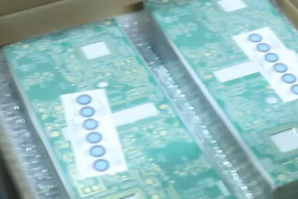
In the years of working on V2G, my deepest feeling is that the board is too easily underestimated. When I first moved into bidirectional charging, my mind was full of topology and control strategy, thinking that as long as simulation ran through and waveforms were clean, the thing was done. Later, when I really threw prototypes into the field to run, the problems all came from the PCB, and the problems that exploded in different scenarios were completely different.
For example, one project was for residential backup power, with installed capacity marked at 7kW, while actual household load seldom exceeded 2kW in the daytime. Our full-load efficiency test results looked beautiful, but as soon as the customer installed it they complained that standby power consumption was too high, eating several dozen kilowatt-hours a month. After a long investigation, the problem was in the power layer design and isolation scheme of the multilayer board. The multilayer pcb manufacturer we found at that time drew it purely as a general industrial power board, without considering the V2G scenario of staying on the grid in standby for a long time. The leakage current path was not handled well, and the auxiliary power supply was always in intermittent oscillation. Later I switched to a supplier that truly understood V2G PCB, re-laid out the creepage in the high-voltage domain, and used partition-potted shielding on the inner layers of the multilayer board, and only then did the standby loss drop to a level that could be handed in. This incident made me thoroughly understand that for a scenario like residential V2H, the core test is not full-load efficiency at all but whether the board heats up, drifts or secretly consumes power on its own in that half-asleep state.
The fleet and commercial park scenario is another matter. We made a batch of V2B charging piles for a logistics park, installed in a concentrated manner on site with piles less than one meter apart, and in summer ambient temperature could rush to above 55 degrees. The first batch of boards began blowing up in batches after two months, and the root cause located was insufficient copper thickness in the DC/DC stage. At the time, to save cost, standard 2 oz copper had been chosen, and the large-current loop’s impedance drifted badly at high temperature, with local hot spots directly burning the solder mask discolored. We hurriedly switched to a Heavy copper PCB supplier, making the key power loop 6 oz or even locally 8 oz Thick Copper PCB, with all vias also backfilled and thickened, and thermal balance was immediately different. Interestingly, after changing the board, not only did the blowing up stop but efficiency also improved by more than one point, because the voltage drop and heat dissipation of thick copper are more uniform. This process made me realize that in a scenario of high-density operation like a commercial fleet, software derating simply cannot cover it, and hard copper thickness is the hard truth, and manufacturers that can stably supply this kind of Thick Copper PCB often differ fundamentally in lamination uniformity and inner-layer resin filling processes.
The challenge of the grid ancillary service scenario is even more of a headache, because the board must withstand not only power but also faults. We took part in a frequency regulation response pilot, which required the inverter to reverse at full power within 200 milliseconds, while the grid side might superimpose instantaneous surges and voltage dips. The earliest prototype used a multilayer pcb supplier that had converted from a communication equipment board factory, and under high di/dt the potential jumping of the control ground plane directly interfered with the logic of the driver chip, causing frequent false triggers during high-speed switching. Later we specifically looked for a Heavy copper PCB manufacturer with high-voltage driver board experience to redesign, strictly separating the drive loop and power loop physically in the stackup, with gate traces in a sandwich structure and the feedback sampling differential pair buried between two grounds. After the change, the fault ride-through type test passed on the first attempt. This shows that making a V2G PCB cannot rely only on the line width current-carrying set; you must think clearly about how the potential at each reference point on the board jumps at the instant of a fault and how the magnetic field cuts.
So now when I look at a Vehicle-to-Grid (V2G) PCB, my first reaction in my mind is no longer topology but three words: scenario first. For the same bidirectional circuit, in a residential scenario you have to work backward from standby power consumption to design leakage and power architecture; in a fleet scenario you have to treat thermal cycling and copper thickness margin as the first design input; and in grid-connected ancillary services, board-level transient electromagnetic compatibility and fault tolerance become matters of life and death. Sometimes when chatting with peers, I find that many failures happen because a so-called universal V2G PCB was forced onto all scenarios, and however good the lab indicators look, it cannot hold up in the field. Finding the right supplier is also not about finding the cheapest, but finding one that can thoroughly discuss the extreme working conditions of the scenario with you at the design stage, especially the key processes of multilayer or thick copper boards, from resin systems to copper foil elongation: a little difference and field performance is worlds apart.
I have been in contact with V2G for several years, and have seen too many people start by fixating on topology and control algorithms, as if tuning a CLLC a bit more beautifully could transform the whole system. This idea is actually quite a hindrance. Anyone who has really crawled on the ground through projects knows that the board printed with all kinds of high-voltage traces is the seven-inch vital point of the whole thing, that is, the Vehicle-to-Grid (V2G) PCB itself. As for efficiency, in the field it is simply not decided by those few percentage points in your simulation. In light-load states, for example when the car is parked at night sending back a few hundred watts to the home, who cares whether your resonant tank waveform looks good? What repeatedly roasts you is the temperature quietly climbing on the copper foil.
Last year I helped a European customer refurbish a batch of returned V2G modules. Taking them apart, the scorched yellow locations were almost all concentrated in the same type of area: on the large-current path, so-called thickened copper was clearly used, yet the local current density at corners and near vias was not contained at all. This is a common failing of many multilayer pcb manufacturers: they stick “heavy copper” onto the spec sheet as a label, while the internal stackup design still follows the inertia of ordinary power boards. When you ask a multilayer pcb supplier for a quote, the other side will say they can make 3 oz or 4 oz, but when it really reaches volume production, the yield drops, resin voids appear during lamination and interlayer withstand voltage problems arise. What you get back is not as good as a board honestly made with 2 oz and fine layout. Later I simply went down into the field myself and fought over routing rules with a manufacturer specializing in Heavy copper PCB for several months, and only then pressed down the problem of sustained heating under light load.
In the end, many people worship Thick Copper PCB as if it could solve all high-current heating, but what is truly fatal is often the “low-efficiency heat accumulation” under light load. At full load for ten minutes, the fan blows hard and heat dissipates fast; what you fear is that your twenty- or thirty-amp board runs all year at only two or three amps, the efficiency curve falls into a pit, heat cannot dissipate, and day after day it dries out the electrolytic capacitors under the PCB pads. My habit now is that for any V2G board, whatever the rated power, I first ask the Thick Copper PCB supplier to show me infrared images of local hot spots from samples running continuously for 4 hours at 10% load. If they cannot produce this data, however thick your copper and however many your layers, I will not pay for it.
There is another point many people do not take seriously: the heating of standby power consumption. Once the car is parked it stays for a dozen hours, communication cannot be powered off, insulation detection cannot be powered off, and these milliwatt-level consumptions simmer on the multilayer board day after day. I encountered the most outrageous case once: in the four-layer area carrying control signals, copper thickness balancing had not been done, causing local stress warpage, and with continuous power on during sleep the board worked in a slightly bent state for most of a year, and in the end the BGA pins of the MCU were cold soldered directly. When I went back to the original Heavy copper PCB manufacturer to pursue the matter, they actually said this was “normal aging.” Since then, my supplier screening has added a hard rule: for a multilayer pcb manufacturer who cannot explain clearly the thermal expansion matching scheme between the mixed-signal area and the power area, I will not even let them make samples.
In recent years the voice that V2G is about to scale up has become louder and louder, but I feel that the seriousness of the whole upstream and downstream toward PCBs is still far from keeping up. When volume production climbs steps in the future, it will absolutely not be enough to buy from a cheap multilayer pcb supplier and muddle through. Light-load efficiency, long-term thermal reliability and interlayer insulation degradation: if any one of these three goes wrong, those who clean up the mess are still us system makers. Besides costing time and energy, the worse part is making end users feel that V2G technology is simply not good, and that loss would be too great.
During the fleet-level V2G project, what gave me the biggest headache was not the control algorithm or the switching logic at all, but how to find a manufacturer that could handle high-current multilayer boards. It may sound a bit strange, but those who have done it will understand: once current rises to several hundred amps, the rules of the whole game change. The board is not only a signal carrier; it is itself a heating body and part of the mechanical load-bearing structure, and a slight slip in heat dissipation means copper blistering and interlayer separation can happen at any moment.
Many people discussing V2G PCBs always place their attention on millisecond-level grid connection and disconnection switching, thinking that is the technological high ground. But my own experience is that however fast the switching, if the underlying hardware cannot withstand repeated thermal shock, the equipment will go down in less than two years. Especially in the commercial vehicle fleet scenario, a logistics vehicle charges and discharges several cycles a day, with dozens of units running simultaneously in the depot. Which Thick Copper PCB supplier dares to pat his chest and say the inner-layer copper thickness uniformity of his board can be within plus or minus 10%? I contacted five or six, and those who truly dare to take heavy copper orders with stable yield can be counted on one hand.
The design of multilayer boards in this kind of product is actually rather awkward. For large-current traces you have to pile on copper thickness, but once the layer count goes up, warpage easily occurs during lamination. The most memorable instance: a multilayer pcb manufacturer prototyped an 8-layer thick copper board for me with nominal 6 oz copper, and when it came back for thermal cycling tests, micro-cracks appeared in the inner layers at around the 300th cycle, causing the backup power test of the entire fleet management system in the workshop to stop completely. Later I switched to another multilayer pcb supplier, who used a stepped copper foil process in the inner layers, and only then was expansion and contraction controlled. This incident let me fully understand that whatever intelligent control and fast switching there is must be built on the bottom line of board material and process.
Another pit with heavy copper is the plated through holes. Many Heavy copper PCB manufacturers, to save trouble, directly use conventional drill bits to process the thick copper layers, leaving hole wall roughness a mess, and once copper plating fills in, stress is all concentrated there. A fleet bumps and vibrates daily, and before the solder joints break, the holes burst first. Once I specifically went to a Heavy copper PCB supplier’s workshop and only then found out that those who truly know the business use step drilling combined with resin plugging, followed by secondary plating and leveling. Boards like that come out with reliability on a completely different order of magnitude. Such details cannot be seen from the specification sheet at all, and can only be found by stepping into pits and auditing factories on site.
Looking back now, articles on the market about V2G PCBs always focus on high-sounding concepts like wide-bandgap devices and hardware dead-time control, but the truest dilemma in front-line engineering is often: you want to make a board that can withstand 200 amps of continuous current while also running high-speed digital signals on it, and there are really not many Thick Copper PCB manufacturers who can do both well. Some factories are good at thick copper but poor in multilayer alignment, and some make multilayer boards beautifully but fail the temperature rise test under large current. At such times you simply have no time for switching speed optimization, and spend all day thinking about how to communicate etch compensation with the board factory and how to control dielectric thickness to balance current carrying and insulation.
What fleet operators value is not how expensive a silicon carbide module you used but how many days a year the equipment runs without failure. In a project I handled, the first 100 V2G terminals were scattered in a bus depot and ran for half a year, and the statistics showed that the part with the highest failure rate was not the power transistor but local PCB burn marks near the high-current screw terminals. Later I changed that small area into an embedded copper block structure and went directly to a Thick Copper PCB supplier to customize a lamination process before solving it. Do you call this some high-level technology? No, but if it is not done well it can bring the whole system down.
Very often, the industry hypes V2G as if it were miraculous, as if as long as grid connection and disconnection switching is handled, everything is fine. But I increasingly feel the real threshold lies in those areas that are not so glamorous, for example whether your PCB supplier is willing, for your small-batch order, to specially tune a thick copper chemical cleaning line, or to reserve several extra hours of cold pressing time during lamination to relieve stress. These things will not be written in papers and will not appear in the PPT of a product launch, but they decide whether the V2G system of your whole fleet can run for ten years or start producing strange problems nonstop after three.
In fleet-level V2G projects, many people start by talking about power topology and silicon carbide, but what actually gives me headaches is the board itself. I mean that Vehicle-to-Grid (V2G) PCB that blends the IGBT or SiC module, drivers, sampling and communication all together. When charging power is pulled up to 11kW or higher, and more than a dozen charging piles run at full power at the same time in a bus depot, the copper thickness and stackup structure on the board directly determine how long the equipment can last.
A few years ago I outfitted a small municipal fleet with V2G equipment, and at the beginning, to save trouble, I casually found an ordinary multilayer board factory to prototype. As a result, in less than half a year, copper peeling began to appear, and some vias had micro-cracks that directly caused signals to go on and off. Only later did I understand that at the 11kW level, a V2G PCB is not something any multilayer board manufacturer can take on. In places with high current, 2 oz copper is not enough, and 3 oz or even 4 oz is what lets people feel safe, and at this time you have to specifically look for a thick copper PCB supplier. But the thermal management and lamination process of thick copper boards are also tied to base material selection and the number of lamination cycles. A good thick copper PCB manufacturer will work out a combination between inner-layer copper thickness and dielectric thickness that matches the thermal expansion coefficients as closely as possible, otherwise once thermal cycling arrives, the resin around the solder joints is soon pulled apart into micro-cracks.
What is most cruel in the fleet scenario is not even the power level but the temperature back-and-forth swings brought by frequent charge and discharge switching. After an electric bus finishes its day, at night it plugs into the V2G pile and first charges hard, and when the grid dispatch command arrives in the early morning it begins feeding power back. The copper conductors on the PCB rush from twenty or thirty degrees to eighty or ninety degrees and fall back within a few hours. This thermo-mechanical stress does not give the board time to breathe. The stackup designed by an ordinary multilayer board supplier according to conventional FR-4 often cannot survive the heating-season dispatching of a single winter. When I place orders with multilayer board manufacturers now, I must explicitly require high-Tg board material, specify the Z-axis expansion coefficient, and require each batch to provide thermal stress test cross-sections. This is not fussiness; it is a lesson learned by losing money.
Interestingly, some manufacturers used to making thick copper PCBs, upon hearing that the application is fleet bidirectional charging, will actually proactively suggest raising the copper thickness one more grade in the installation areas of electrolytic capacitors and transformers. They have seen too many cases of copper foil peeling from the base material due to local overtemperature. Moreover, at the routing level, in an 11kW V2G loop, if the DC bus copper thickness is insufficient, the equivalent resistance is only one or two milliohms higher, and the efficiency of the whole charge drops a little. In a depot with thirty charging piles, over a year it is a considerable waste of electricity. So looking for a thick copper PCB supplier is not about how big the factory is, but whether it is willing to work with you on those few critical safety distances and copper thickness margins.
In a recent project we were even pushed to directly use the embedded copper block process to handle the hottest switching transistors on the V2G board. The heat dissipation is good, but there are really not many thick copper PCB manufacturers who can do this job beautifully. In short, in the matter of V2G, the choice of multilayer board supplier almost decides the actual usability of a fleet-level project, since however good the topology, soldered onto a board that cannot withstand thermal shock, it is all in vain.
In the matter of V2G charging piles, many people stare at power devices and software algorithms, but after tinkering for these two years, my biggest feeling is that PCB selection and manufacturing directly determine the life and death of the project. It is not that other links are unimportant, but that when that ten- or twenty-kilowatt of bidirectional conversion power runs back and forth on the board, once the copper cannot hold or the heat dissipation channel is designed carelessly, efficiency and lifetime are all empty talk.
In the stage of looking for a multilayer pcb manufacturer, I ran into a wall right away. At first I thought an 8-layer board with 2 oz copper thickness could be made by any supplier, and when the prototype came back and ran at full load, under the infrared thermal imager the copper foil temperature directly soared to more than a hundred degrees, and the via area near the MOSFET was as hot as a soldering iron. When I tore it open and cut a section, I found that the inner-layer copper thickness had simply not been made sufficient, and the via copper in some vias was ridiculously thin, so heat simply could not be carried away. Later I switched to a factory that specializes as a Heavy copper PCB manufacturer, who treat 4 oz copper as standard, and who also optimized the lamination order, sandwiching the high-current layer in the middle with thick copper ground planes above and below, so the whole PCB is like a fixed heat dissipation skeleton. That feeling of steadiness as temperature runs down evenly can only be understood after measuring and comparing.
The trouble with thick copper lies in etching precision. On an ordinary board, trace spacing can be pressed to 5 mil, whereas Thick Copper PCB line width compensation needs several days of confirmation back and forth with the manufacturer, because with copper so thick, the undercut effect makes line width considerably smaller than the design value. I forced my engineers to hold three online meetings with the process department of the Heavy copper PCB supplier before figuring out the actual offsets of exposure and etching on their production line. That was not all. Solder-mask-coated thick copper boards also easily blister, and not just any multilayer pcb supplier has the experience to handle this well. Later I settled on a Thick Copper PCB manufacturer who could both do thick copper and control impedance, and only then did I press the power loop stray inductance down to the nanohenry level, and the swallow-like ringing at the switching node was finally pinned down.
The harmonics pit is something many people think is a matter of software strategy or filter parameters. But in testing multiple V2G units on the grid, I found that with the same control code and the same LCL values, changing one PCB could make the THD at the point of common coupling differ by half a percentage point. The root cause is in the layout: the overlapping area of power loops and signal loops, and the jitter ground bounce noise puts on PWM signals, parasitic parameters you cannot see that directly stuff harmonics into the grid. When I used to debug a single unit, getting output current THD down to around 2% felt pretty good. Later, when I hung twenty Vehicle-to-Grid (V2G) PCBs under one transformer to run, the aggregated harmonics could gnaw burrs into the voltage waveform. I did not go for any centralized carrier phase synchronization, but instead started from the V2G PCB itself…
To put it plainly, the thing called V2G: the harmonics the grid side sees you injecting are essentially an amplification of the power conversion traces on your board. Rather than painstakingly remedying at the point of common coupling, it is better to force the Thick Copper PCB supplier to make the board uniform in both heat and electricity. My attitude toward the V2G PCB is now very clear: it is first a structural component, and only second a circuit carrier. Copper thickness, layer count, via filling and board material heat resistance rating: these parameters are not options but the bottom line for survival. Finding the right multilayer pcb manufacturer and letting the copper truly work for you, rather than becoming a heating wire, is more fundamental than agonizing over which brand of SiC module to use.
In the several years I have worked on grid-side ancillary services, I have found that many people in this circle put all their attention on protocol response speed, repeatedly optimizing the command delay of those few hundred milliseconds, while neglecting the most basic physical reality. The V2G main loop is not a signal link in a laboratory; it is copper skin and insulation layers truly carrying large power back and forth. After repairing several boards returned from the field, I settled on one thing: when power and current reach this magnitude, the physical structure of the PCB touches the ceiling before the control strategy does.
Put another way, if you do not find the right multilayer pcb manufacturer, everything afterward is empty talk. When grid frequency regulation has to inject tens of kilowatts of reactive power into the grid, if the copper is not thick enough, current density can instantly heat the traces to discoloration and blistering. This is not a matter of calculating how many layers the board has, but of explicitly telling the supplier that the through-current peak of my busbar group will rush to 80A or even 120A and thick copper is needed to share the thermal stress. For this reason, after paying dearly early on, my eye for choosing a Heavy copper PCB supplier became especially picky. It is not that anyone who can make 2 oz copper is called a thick copper board maker. In a real V2G PCB scenario, only a Thick Copper PCB manufacturer with 4 oz inner layers, 6 oz outer layers, or even local 10 oz can hold the temperature rise under instantaneous large current. Otherwise, when thermal cycling arrives, the CTE mismatch between copper foil and base material tears the vias open, and the whole board is scrapped directly.
There is another seriously underestimated problem: how to physically separate the power loop and the control loop cleanly. We have all seen cases where the schematic is drawn beautifully, but after the actual layout the stray inductance is a mess. V2G ancillary services frequently trigger charge and discharge switching, and this transient bounces the ground plane around chaotically. My approach is that, right from the start when settling the stackup with the multilayer pcb supplier, I separate the power ground and signal ground with thick copper inner layers, join them at a single point, and have the Thick Copper PCB supplier thicken the copper of the power traces, taking care to use rounded transitions at the edges to avoid tip discharge. This is the true path that turns the “trip” in the protocol into a physical fact: the data measured by the local current sensor, plus a hard copper loop, is what lets you say that cutting off truly means cutting off. Without this layer of hardware confidence, however beautiful the communication protocol sounds, it hangs in mid-air.
I have been doing V2G hardware for a while, and I increasingly feel that this circle puts too much energy into that so-called “independent protection path” and neglects some more fundamental things. Everyone talks about hardware logic directly driving the contactor open when overcurrent is detected, which sounds especially rigorous, but after actually drawing several versions of the V2G PCB, you understand that what really makes this path work reliably is often not the logical architecture but the copper thickness, stackup and process capability of the manufacturer you choose.
This is exactly where I paid. One prototype had a protection path with completely independent logic and isolated power, theoretically watertight. But after running in batches, it occasionally false-triggered even when the rated current had not reached the threshold. After more than half a month of checking, I found the problem was not in the comparator or the sensor at all but that temperature rise on the PCB busbar produced a thermal gradient near the Hall device and the signal drifted. That board used conventional 2 oz copper, with trace widths calculated according to the manual, but it could not stand tens of amps flowing back and forth continuously, and heat was all accumulated in the inner layers. Thinking back, if I had found a reliable heavy copper PCB manufacturer from the start and used thick outer copper directly to carry the current, while reconsidering the sensor layout, I would not have wasted time for nothing.
When I redid the order, I changed my thinking. When I talked to a multilayer pcb supplier about requirements, I clearly said I wanted a 6-layer board with hybrid inner and outer copper thickness: 4 oz on the outer layers for the large-current path and 1 oz on the inner layers for signals. Not every factory can handle this hybrid lamination. A multilayer pcb manufacturer with a good reputation told me directly that when the copper thickness difference during lamination is too large there is warpage risk, so lamination parameters and layout must be adjusted, with extra temperature measurement points added. It was just for this honesty that I gave them the order. When the board came out and I measured the internal resistance, it was nearly half of the old version, and under the same load the busbar temperature rise was controlled within 15 degrees, and the inexplicable false alarm disappeared completely.
Frankly, by the end my understanding of this hardware path in V2G had changed. It is not just a group of traces from sensor to comparator to driver, but a continuous physical channel, starting from the DC-side contactor pads, passing through busbars, copper foil and via arrays, and then reaching the solid state switch on the AC side, with every step part of the path. Many design failures come from looking at this path in a fragmented way: caring only about the “cleanliness” of the logic signals, without managing those few key necking points on the large-current loop. Insufficient current-carrying margin in vias, corners of copper skin without arc transitions, and even the location of solder mask openings affecting heat dissipation can make a finely designed protection logic fail on the physical layer.
Now, when I chat with peers, I generally advise them: do not start by agonizing over how mysteriously to isolate the cut-off logic; first sort out your multilayer board supplier and thick copper board supplier. Finding a factory that can make heavy copper PCB, or at least finding a thick copper PCB manufacturer willing to work through thick copper process and stackup balance with you repeatedly, is more practical than anything. After all, V2G hardware runs on the road. It is not an ideal circuit in a laboratory, and all protection paths are ultimately held up by copper and base material on your behalf.
In the years of working on onboard charging and V2G, I increasingly feel that a reliable board is not supported by some divine chip but depends on how you deal with those invisible parasitic parameters. Many people start by chasing SiC module swaps, thinking that once silicon carbide is used, efficiency naturally goes up, but if the board itself is drawn badly, even the best transistors on top are in vain.
I stepped into a pit last year on an 11kW bidirectional OBC project. At that time I found an ordinary multilayer board supplier for prototyping, and as a result the switching node ringing was so large that I did not dare to raise it to rated voltage, and in the end I still went back to find a manufacturer that could make heavy copper and re-ordered the board. Many people may not know that in a V2G situation where long-term full-power bidirectional running is needed, if the main power traces are even slightly thinner, it is not only a heating problem: when the current change rate is large, the distributed inductance of the copper foil makes your turn-off spike ridiculously high. We later added inner-layer copper thickness to 4 oz and used embedded copper process directly for some commutation loops, and only then was the spike barely pressed into the safe range of the SiC transistors. Honestly, there are not many manufacturers who can handle this kind of thick copper PCB, and many manufacturers who claim to do heavy copper only thicken the outer layer, while the inner layers remain at conventional thickness, which is useless.
Another headache is isolation. SiC switches so fast that dv/dt easily reaches a hundred volts per nanosecond, and if the common-mode transient immunity between the primary and secondary of the isolated driver is insufficient, a pulse passes and gives you a false signal. I tried adding ferrite beads and extra common-mode chokes in the gate loop, but the best effect still came from cutting off the coupling path through board layout. No copper can be laid under the driver, and the slot width must be calculated from actual dielectric strength, not copied from a reference design. Sometimes, to satisfy the creepage distance of reinforced insulation, the board area has to be enlarged by nearly a quarter, which is fatal for automotive equipment, but there is no way: safety cannot be compromised.
The control and sampling part actually has fewer mysteries. The bandwidth of the voltage and current sampling chain reaching above 500kHz depends on the slew rate of the front-end op amp and the complete reference plane layer within the multilayer board stackup. I have seen manufacturers use a six-layer board for V2G control, mixing analog ground, digital ground and power ground into one pot, and as a result 50Hz harmonic content exceeded limits during grid connection. It is not that the stackup advice given by the multilayer board supplier is wrong, but that you yourself have to be clear which signal references which, drawing the return path tightly. Our practice now is to put the analog parts of sampling and DAC in an interlayer, with complete ground copper wrapping above and below, and then punch a ring of isolation holes outside, so that immunity can be improved by several orders of magnitude.
In the end, the reliability of a V2G board is ground out under extreme grid conditions. The fault ride-through, reactive power regulation and anti-islanding written in the standards, when they land on hardware, are a pile of logic chains that must be independent of the main controller. I tend to build the passive anti-islanding judgment circuit out of a comparator alone, and once triggered, directly lock the pulses without going through the MCU’s software flow. The benefit of this hardware redundancy is that when problems occur you do not have to suspect whether the software has run away. Such detail-level dedication is the true watershed between a reliable V2G PCB and a board that can only run prototypes in the lab.
When making hardware for bidirectional charging and discharging like V2G, very often the problem is not in the topology but hidden in the details of the PCB. I have a habit when doing this kind of board: before prototyping, I always settle the stackup structure with the multilayer board supplier first, especially when there is a DC isolation requirement, where the insulation thickness and dielectric constant between layers drift the isolation withstand voltage with even a slight deviation, which is very troublesome.
Many people think isolation is just placing a few isolation chips and pulling a split slot and being done, but in fact how the whole ground plane under the isolation barrier is handled directly affects the path of common-mode noise. I generally paste the isolated power module on the driver side right next to the transistors, and that board must be of thick copper process, at least 2 oz up, and if the power is a bit larger, go directly to 3 oz or even 4 oz thick copper boards. Finding a reliable heavy copper PCB supplier is actually quite difficult: quite a few manufacturers claim to be able to do it, but the finished copper thickness is uneven, edge thinning is serious, and large current makes them heat up. Later I simply fixed on the heavy copper PCB manufacturer we had worked with for a long time to bed in, whose lamination and etching control is steadier and whose finished product consistency is good.
I have also stepped into pits with sensors. Current sensing in V2G needs not only accuracy but also linearity maintained in both directions. Although Hall sensors placed directly on a high-voltage busbar are convenient, their zero drift is too sensitive to temperature, and especially when running large current for a long time in DC charging mode, after temperature rise the metering accuracy clearly slips. Later we changed to a shunt scheme with an isolated amplifier, but the requirements on PCB routing became higher, with the Kelvin connection at both ends of the sampling resistor needing to be symmetric, and if the differential routing is even slightly longer, the introduced inductance can distort the signal. So when I draw this kind of sensor circuit, I directly ask the PCB factory to make a multilayer board of six layers or more, burying analog channels separately in inner layers, wrapped above and below by complete ground layers, and running the power layer outside, so signal integrity and isolation effect can both be taken care of.
Speaking of the current path of the V2G PCB, I have used boards from thick copper PCB suppliers to handle many continuous currents at the hundred-amp level, but wider traces are not necessarily better. During high-frequency switching, the skin effect concentrates current on the surface, and simply widening is meaningless. Instead you have to communicate with the multilayer board manufacturer to match copper thickness and line width, and sometimes even parallel the traces in layers so that current distributes more uniformly. If this communication is not in place, the board that comes back can never reach the simulated value in performance.
For the isolated power supply, the DC high voltage in a car often reaches eight hundred volts or even higher, so the onboard isolated DC-DC module cannot be selected casually, and leakage capacitance must be controlled at the picofarad level, otherwise the transients coupled across will break down the digital-side devices. I generally mark the slot width of the ground planes’ separation explicitly on the mechanical layer and then have the manufacturer’s engineering confirm whether complete separation can be achieved. Otherwise creepage distance is insufficient, and the withstand voltage test breaks down directly. These details must be spelled out when dealing with a thick copper PCB manufacturer, otherwise for process convenience they may leave tiny connections for you, and it explodes when powered on.
In short, for hardware like V2G, the PCB is not a simple wiring carrier; it is itself part of the device, and especially in the isolation and power loops everything depends on the board itself to bear. Choosing the right multilayer board supplier and heavy copper PCB manufacturer can really save more than half of the trouble in the later debugging stage.
When I took over a charging pile retrofit project last year, I truly realized that the Vehicle-to-Grid (V2G) PCB is far from just putting high voltage and low voltage together on one board. In the earlier unidirectional charging work, the current path was single, and heat dissipation and routing were basically routine work. But once you want power to flow in both directions, especially to support the residential backup power scenario, any inconspicuous parasitic parameter on the PCB gets amplified. I remember that when the first prototype came back, the switching transistor ringing was ridiculously large, and after measuring I found it was because the four-layer board’s layout had not handled the power loop well. In an instant I felt my little experience had been slapped in the face.
Later I turned around and reselected materials, and only then understood that some money really cannot be saved. For the large-current zone on that board, I specified thick copper directly and looked everywhere for a Heavy copper PCB manufacturer, compared several before settling. At that time a domestic Heavy copper PCB supplier patted his chest and said 4 oz copper thickness was a piece of cake, but the sample that came out had insufficient copper adhesion at the edges and had cracked during sintering, and I blacklisted them directly. This incident taught me a very simple lesson: when choosing a Thick Copper PCB manufacturer you cannot look only at the specifications on the quotation; you must really go and run their production line once, look at how the corners are handled in actual output, and look at the glass transition temperature test data. Later I switched to a Thick Copper PCB supplier that began in industrial power supplies and directly used 6 oz inner layers, and after the copper thickness went up, the temperature rise problem was relieved by more than half.
V2G has another pit that is especially easily overlooked, which is the isolation between signal layers and power layers. The control pilot line carries low-voltage signals, but it is connected directly to the outside-of-vehicle interface, and surges and static come in without any reason. I started with an ordinary multilayer board and set the isolation spacing at 1 millimeter by general rules, and as a result when doing the surge test the communication chip failed directly. At this time a knowledgeable multilayer pcb supplier reminded me that a complete protection ring must be made at the communication connector entrance, and that the common-mode choke must be moved forward to the position nearest the pins, with spacing enlarged to at least 3 millimeters to be stable. After taking this advice, I went back to a multilayer pcb manufacturer to change the board, and only then did the immunity of the communication link reach a level that could pass certification.
Thinking back now, the design of a V2G PCB is essentially negotiating with the limits of physics. On one board you need to take care of instantaneous current of several hundred amps and millivolt-level weak signals, while also ensuring no leakage between the always-on domain and the controlled domain, and the standby leakage current really must be at the microamp level to meet the energy consumption requirements of the residential scenario. When you face a specific project, all of these translate into an interrogation of the factory’s real capability. When choosing a Heavy copper PCB supplier, you must ask whether he has made bidirectional topology boards, and ask clearly whether his dielectric layer thickness tolerance can stay stable under repeated thermal cycling. And when choosing a multilayer pcb supplier, I value more whether they have handled mixed-signal high-power board experience, because in this scenario conventional module partitioning alone is simply not enough, and a lot of interference conducts from the stackup structure itself. In the end, a qualified V2G PCB is not counted once designed; it is verified by the factory’s real process.
Many people think the difficulty of landing Vehicle-to-Grid (V2G) is too narrow, starting right away by agonizing over topology selection or communication protocols, while seldom noticing how the circuit board itself holds up in real scenarios. I have seen far too many schemes run well in the lab, then on arriving in the garage of an old residential community have problems in the whole bidirectional charging and discharging loop because of chaotic grounding. This has nothing to do with software algorithms at all, but with the layout of those few groups of sensing lines and the thick copper traces on the V2G PCB. I used to think that finding a reliable multilayer pcb manufacturer to do the stackup well was enough, but later I found that it is far from enough. A multilayer board can indeed help you separate the power loop from the signal layers, but once you ignore creepage distance requirements, the board produces micro-leakage after several condensation cycles, the zero point of isolated current sensing begins to drift, the current direction read by the main controller becomes confused, and energy scheduling is entirely disrupted.
So I now tend to work backward from the scenario when making board-level decisions. For example, in a fleet-aggregating V2G pile, the board runs at full power all year, heat accumulates quickly, thermal cycling is frequent, and ordinary copper thickness simply cannot withstand long-term expansion stress. At this time, looking for a Heavy copper PCB supplier is not just simply for enough current carrying, but because thick copper can lower temperature rise, delay fatigue of solder joints and reduce loss from inner-layer resistance. Some will ask about cost, but I have calculated that using 4 oz and above copper foil provided by a Thick Copper PCB manufacturer is actually more cost-effective when spread over the whole life cycle of failure repairs, not to mention avoiding the hidden losses of unexpected downtime. There is also an easily skipped link here: the sensing signal acquisition around the high-current path. You cannot put the op amp far away and then pull a thin wire over, because electromagnetic interference would swallow up the true waveform completely. You must put the analog front end of isolated current sensing right next to the shunt or Hall element, and the reference ground must return in a single point to the thick copper area, so that linearity in both charging and discharging directions can be preserved.
Of course, the complexity of V2G also lies in the fact that it plays completely different roles in different applications. Residential backup power scenarios emphasize quietness and standby power consumption, and at this time the always-on domain design of the V2G PCB must do subtraction: circuits that should be turned off must be completely cut off, while the communication controller must stay awake waiting for commands, so the power tree partitioning on this board must be drawn very clearly. Grid ancillary services are different: the response speed requirement goes to the millisecond level, and the SiC drive loop on the board must be minimal. If the gate loop area is even slightly larger, the voltage overshoot generated at turn-off may falsely trigger protection or even damage the power transistor. After years of repeatedly prototyping with several multilayer pcb suppliers, my biggest takeaway is: do not trust universal solutions. Boards in each scenario should have their own skeleton. Precisely because sensing, driving, communication and current carrying all compete on the same board, finding the right supplier is not the end point. Being able to weigh these contradictory details from a system perspective yourself is the core that makes bidirectional energy flow truly reliable.
Anyone in RF knows the Distributed Antenna System PCB in an in-building
A trailer brake controller suddenly lurches, and after hours of checking the
Microwave Backhaul PCB failures often start in lamination and etching, not the
- Experte für die Produktion kleiner bis mittlerer Chargen
- Hochpräzise PCB-Fertigung und automatisierte Montage
- Zuverlässiger Partner für OEM/ODM-Elektronikprojekte
Geschäftszeiten: (Mo-Sa) von 9:00 bis 18:30
Get quote, solution or any question, Andre always here to help