

The Success Illusion of Prototype PCB Production: Why a Bidirectional DC-DC Converter PCB Works as a Sample but Fails at Volume
Chasing perfection at the Prototype PCB Production stage can actually plant hidden
I’ve always felt that the most fascinating stage of circuit board work is prototyping. Watching an idea go from a sketch on paper to something you can actually hold in your hand is a process full of the unknown and full of surprise. A lot of people, when they hear “circuit board prototyping,” picture high-end equipment or complicated workflows. That’s not necessarily true. Sometimes the simplest tool is actually the best fit for quickly validating an idea.
I remember the first time I tried building an audio amplifier, I skipped the breadboard stage entirely. I figured soldering was too much hassle and it would be faster to just draw the PCB directly. The boards came back and I discovered I’d picked the wrong capacitor value, scrapping the whole board. That experience taught me that projects of different complexity genuinely need different prototyping approaches.
These days, for simple digital-circuit debugging, I still default to perfboard. The solder joints don’t look pretty, but modifications are especially flexible. Last week, debugging an infrared sensor, I swapped in three different receiver models on the perfboard before finally determining which had the strongest interference resistance. That kind of anytime-adjustment convenience is something formal prototyping just can’t offer.
Of course, when high-frequency signals or precision analog circuits come into play, the situation is completely different — exactly the territory where a genuine high Frequency PCB supplier earns their keep. For example, last year, working on an RF module, I tried hand-etching a board, but the results were poor. I ended up going to a professional manufacturer for an impedance-controlled four-layer board. It cost two extra weeks, but the test results passed on the first try. In situations like that, trying to save cost actually delays the overall timeline — a lesson that applies directly to something like an Automotive LiDAR PCB, where signal timing and impedance margins leave almost no room for guesswork.
Some engineers I know get especially attached to a single prototyping method. In reality, every method has the scenario it fits best. What matters is being clear about exactly what you need to verify right now — functional stability, signal integrity, or mechanical structure. Sometimes you even need to combine methods, like running a software simulation first and then building the physical prototype.
Recently I’ve been trying to combine 3D printing with traditional PCB work for a wearable device — printing a curved resin housing first, then embedding a flex circuit into it. This kind of hybrid prototyping approach has noticeably sped up product iteration. That said, soldering flex boards genuinely requires more patience — even a moment’s carelessness can scorch the substrate.
At the end of the day, prototyping is a lot like building with blocks — there’s no single correct formula. What matters is keeping the courage to get hands-on and the flexibility to try and fail. Every time I see an LED blink on schedule exactly as planned, that sense of accomplishment always reminds me why I love this line of work.
My own experience prototyping circuit boards has been genuinely interesting. When I first got into electronics fabrication, I always assumed I needed to nail the final product in one shot. I later found that repeated revision is actually the norm. Once, for a simple sensor module, I went through seven or eight versions total, each time because the layout or routing needed adjustment.
Using CNC for prototyping is genuinely convenient, especially when you need to quickly validate an idea. I remember one weekend at home, suddenly thinking of a circuit improvement, drawing it up in software and immediately starting to mill it — by evening I had a physical unit to test. That instant-feedback feeling is great, far more flexible than waiting on a factory sample run.
That said, milling has its limitations too. Handling double-sided boards, for example, is fairly troublesome — via precision is hard to control well, and sometimes the bit breaks, which actually wastes time.
Many people find hand-soldering a hassle, but I actually enjoy the process, especially using a small knife to cut copper foil bit by bit — it feels like doing craftwork. It’s not efficient, but it genuinely helps you understand circuit structure.
I now prefer combining different methods, choosing the right approach based on the project stage — a simple perfboard for early validation, CNC for a single-sided board once things get a bit more complex, and only sending it to a factory for board-making once you actually need stable testing. This way you save cost while still keeping the project on schedule.
Actually, the thing to fear most in circuit design is falling into the perfectionism trap — always wanting to get it exactly right the first time, which actually slows the whole project down. Sometimes a rough working prototype is worth more than a perfect drawing, because it tells you what genuinely needs improvement instead of staying purely theoretical.
I’ve seen quite a few beginners spend too much time on software simulation without daring to build the physical thing, only to run into real-world problems completely different from the simulation results. Whatever you build by hand, however crude, gives you the most honest feedback — and that’s really the biggest value of prototyping: not chasing perfection, but fast trial-and-error and fast learning.
Working on my own electronics projects, I’ve noticed an interesting phenomenon — a lot of people jump straight to designing a perfect PCB fabrication file, when in reality the initial idea stage doesn’t need to be that complicated.
I remember once wanting to build a simple temperature-controlled fan, and I just plugged a few components straight into a breadboard to test it out. This kind of perforated plastic board is especially well suited for quickly assembling a circuit — you just push component leads into those small holes to rapidly validate an idea.
That said, breadboard connections really aren’t very stable — the slightest bump can cause poor contact.
I later switched to perfboard with soldering pads for a more durable prototype. This kind of board has metal pads arranged neatly across the surface — you thread component leads through and solder them in place.
The soldering process is genuinely therapeutic — watching each component get fixed in place, the circuit connection becomes far more reliable.
Once, I used perfboard to build a music-box circuit. Although the wiring looked like a spider web, the actual result was far more stable than a breadboard.
These days, when doing circuit board prototyping, I typically go in two steps: first use a breadboard to validate whether the core function is feasible, then use perfboard to build a testable physical prototype.
A recent LED dimmer I made for a friend was built this way — spending three days on the breadboard tuning circuit parameters, then finally soldering a sturdy sample on perfboard for him to try out.
This kind of step-by-step approach avoids getting bogged down in PCB design details right from the start, while still ensuring the final product’s reliability.
The biggest lesson from all my years doing circuit boards myself is: never rush to chase perfection at the prototype stage. Many people jump straight into wanting the circuit board design to look like a work of art, which actually tends to slow progress down.
I remember when I first started doing circuit boards, I obsessed over every single component’s placement, wanting the routing laid out as neatly as a textbook diagram. I later realized this kind of perfectionism really isn’t necessary — a prototype exists to make mistakes on. Once, I spent several days revising what seemed like a perfect layout, only to find during actual testing that a critical signal needed rerouting entirely — all that earlier effort wasted.
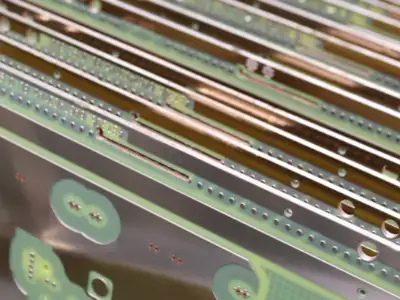
What genuinely matters is validating the idea quickly. Now, when I prototype, I always get the function working with the most direct approach first, even if the wiring looks a bit messy — that’s fine. Only once the core function is confirmed working do I consider optimizing the layout. This mindset has saved me a lot of detours. For example, when validating a power-management module, I’ll first build the basic circuit on a breadboard, confirm the voltage-conversion efficiency meets spec, and only then move on to PCB layout. This staged verification approach effectively avoids wasted resources from over-engineering.
The process from circuit board prototype to mass production is really one of continuous simplification. Early on, you can go wild with jumper wires and last-minute changes — that’s all normal. But the further along you get, the more you need to factor in manufacturing feasibility.
Once, I designed a particularly elegant circuit board using quite a few special components, only to discover, when preparing for mass production, that one of the components had unstable supply, nearly delaying the entire project. From then on, whenever I design, I always check component availability first. Now I maintain a library of commonly used components, prioritizing generic models with multiple suppliers, and I leave pad footprints for alternative components. This kind of design redundancy does increase the initial layout difficulty, but it significantly improves mass-production adaptability.
What mass production truly tests is design stability — not how novel the idea is, but whether every single board can meet the same standard, which requires extensive testing work upfront. Sometimes, for what seems like a minor detail, we might need to adjust repeatedly several times until finding the most reliable solution. For example, during high-temperature aging testing, we once found a certain capacitor’s capacitance degraded beyond acceptable limits after 200 hours of continuous operation, and we ultimately solved it by switching to a more heat-resistant model.
I think a lot of people today rely too heavily on software simulation, always thinking they can solve every problem on the computer, but the actual assembly process always runs into the unexpected.
Just last week, I ran into an example: the simulation showed a clean signal, but actual testing revealed interference. It eventually turned out a particular ground point’s position needed fine-tuning — this kind of problem is simply impossible to discover without hands-on work. During actual debugging, we also found simulation software can’t fully replicate real-world electromagnetic compatibility issues — for example, when a circuit board is mounted inside a metal enclosure, the effect of the ground loop is far more complex than the simulation result.
So now I place great emphasis on physical testing — even for the simplest circuit board, I still personally solder and debug it. This process takes time, but it uncovers a lot of potential issues. Sometimes a tiny adjustment can significantly improve the overall circuit’s stability. For example, adjusting the placement of a decoupling capacitor can reduce power-supply noise by more than 30% — an optimization you can only accurately grasp through actual measurement.
Speaking of going from prototype to mass production, a lot of people think of it as a linear process. In reality, it’s more like an upward spiral. You may need to switch back and forth between the lab and the production line several times, continuously refining details.
We’re currently working on a project where, during the trial-production stage, we found a component’s soldering process needed adjustment. It was just a small temperature-setting change, but it directly affected the finished-product yield — this kind of experience simply can’t be accumulated without actually reaching the mass-production stage. We also found that the dielectric constant of PCB material varies slightly between batches, which requires targeted fine-tuning of the matching network for high-frequency circuits.
At the end of the day, the most interesting part of making circuit boards is that it connects creativity to reality. You have a good idea, and through a circuit board it becomes something tangible and touchable — that process itself is full of appeal. What matters is staying open-minded, willing to keep adjusting through practice, rather than rigidly sticking to the original design plan.
I’ve always found circuit board fabrication a genuinely interesting subject. A lot of people, when they hear “circuit board prototyping,” immediately think of outsourcing it to a professional factory. In reality, doing it yourself can actually reveal a lot of unexpected details.
I remember once trying to make a small gadget using milling, and at first I always felt the precision wasn’t good enough. I later realized the problem wasn’t the machine itself — it was that I didn’t understand the material’s properties well enough. For example, copper-clad laminates of different thicknesses require very different milling parameters — that’s an experience you simply can’t learn from any number of tutorials.
3D printing is popular on the market right now, and it’s genuinely convenient, but I think it’s better suited for structural parts like enclosures. For actual circuit prototyping, traditional subtractive manufacturing is still more reliable. After all, conductivity performance is something you can’t be careless about — the connection quality between layers directly determines success or failure.
I’ve seen people, to save effort, directly extrude conductive material with a 3D printer, only to end up with trace resistance absurdly high. That kind of prototype is only good for looking at — it’s completely unusable for actual testing. So now I’d rather spend more time slowly fine-tuning on a milling machine, at least ensuring every pad is genuinely solid copper foil.
Of course, self-made prototypes do have limitations, like not being able to handle overly complex multilayer boards. But that actually forces me to think more thoroughly at the design stage, instead of always counting on stacking more layers later to solve problems. This kind of constraint can actually be a good thing — it cultivates a more rigorous design habit.
I recently tried combining milling with hand soldering and found the results unexpectedly good. Although it adds a few extra steps, the finished product’s reliability improved noticeably. This hybrid approach made me realize there’s no absolute good or bad in manufacturing processes — what matters is how you combine them.
At the end of the day, what makes prototyping so fascinating is precisely its uncertainty. Every attempt at a new method feels like solving a puzzle — it might fail, or it might surprise you. This process of turning an idea into a physical object with your own hands is probably an engineer’s greatest joy.
Every time I get a newly designed circuit board, I feel a bit like I’m unwrapping a present. That small board carries so much possibility — it could be the nerve center of a smart-home device, or it could be the heart of an industrial controller, or, in demanding cases, an Automotive LiDAR PCB that has to hold precise timing in a vehicle’s sensing stack. A lot of people think a circuit board prototype is just for show, but it’s really more like a carefully choreographed dress rehearsal.
I’ve seen quite a few teams skip thorough prototype validation to save time on schedule, only to discover signal-interference problems at mass production and be forced into rework. Once, we designed a motor-drive board, and everything looked perfect in software simulation — the same discipline a high Frequency PCB manufacturer applies when a design pushes signal timing to its limit. It wasn’t until the physical unit came out that we discovered the heat sink’s position blocked a connector — it took two full weeks of debugging to find a compromise. That lesson taught me that no simulation, however refined, can replace the real feedback of touching a component with your own fingers.
Now, when prototyping a circuit board, I place much more weight on its communication value. A hardware engineer can use it to show a structural designer where interfaces sit, a project manager can use the physical unit to estimate assembly time, and even a customer can get an early feel for the product in hand. I remember once bringing a prototype with visible jumper wires to a user test, and the person pointed at a particular button, saying “this position feels awkward under my thumb” — that single comment led us to redesign the entire panel layout, saving a huge tooling-modification cost down the line.
Of course, the ability to iterate quickly has genuinely changed the rules of the game. Last year, developing an environmental-monitoring device, we revised the circuit board three times in a single week, adjusting everything from sensor type to power supply scheme based on real test data — that kind of agility would have been unimaginable in the traditional manufacturing era. That said, I’ve also found that sometimes slowing down is actually better. Once, we deliberately slowed the pace, spending two weeks purely optimizing the power-management section, and the final battery life came in 30% higher than competing products.
At the end of the day, a circuit board prototype isn’t an endpoint — it’s a starting point. It gives you the chance to make mistakes, to adjust, even to scrap and start over, before committing to large-scale production. What’s genuinely valuable isn’t the board itself — it’s the room for thought it creates. Behind those blinking LEDs and jumping data lies the entire secret of a product’s journey from concept to reality.
Every time I see those neatly arranged circuit board prototypes, I think back to when I first got into electronics design. Back then, I assumed that having an idea meant you could go straight to a finished product. I later realized there’s a repeated refinement process in between — just like a building can’t skip its foundation, circuit board fabrication also needs to go through different stages of validation to ensure the final product’s reliability.
I’ve seen quite a few people rush things, skipping the critical prototype-validation step, only to have the whole project end up in rework. The thing to fear most when making circuit boards is assuming things will just work — thinking the theoretical calculations check out and jumping straight into production, when actual application always runs into unexpected situations, like signal interference or power fluctuation. These small problems are completely invisible on a drawing; only by actually building it can you discover them.
I remember once helping a friend debug a simple control board. He’d already drawn the design and planned to go straight into small-batch production. I suggested he first build a simple circuit board prototype to test it, and sure enough, during debugging we discovered a chip’s supply voltage was unstable. Had he gone straight into production, that entire batch of boards might have been scrapped. That experience made me even more convinced that no matter the project’s size, you can’t skip this step.
More and more teams today recognize this and schedule multiple rounds of validation before formal production, resolving potential issues in advance. Although this adds some upfront time cost, it actually saves far more resources in the long run. I think of this process as buying insurance for the design — it seems like extra effort, but it avoids much bigger losses.
Sometimes, looking at those component-covered prototype boards on my desk, I feel like they’re not just circuits — they’re more like a necessary stage in a product’s growth. Every adjustment and improvement along the way lays the groundwork for the final result. That kind of grounded feeling is something you simply can’t get by skipping the process.
Every time I see an article that makes circuit board development sound especially mysterious, I find it genuinely amusing. In reality, once you’ve been in this business long enough, you realize what’s truly interesting was never the standard procedures — any engineer can recite those from memory. What I actually find valuable are those moments that seem to break the usual rules.
Remember that smart-home project from last year? At the time, a newly hired engineer on the team insisted on following the textbook steps for circuit board prototyping. Guess what happened? The very first version got stuck on the power-management module. We all laughed at how rigid he was being at the time. Actually, the biggest taboo in hardware development is exactly this kind of linear thinking. For example, in the power-management section, he strictly selected component parameters based on theoretical calculations, but overlooked the effect of actual operating temperature on component performance, resulting in voltage instability during high-temperature testing. This kind of detail often needs to be adjusted based on on-site test data, rather than relying purely on formula calculations.
I’ve seen too many people treat circuit board prototyping as a process that must be followed rigidly. But honestly, the teams that actually produce breakthrough products tend to find inspiration precisely in seemingly chaotic experimentation. Like that project we later shifted to a test-as-you-design model, which actually finished two weeks ahead of schedule. Specifically, we adopted modular parallel development, letting the RF team and power team run prototype validation simultaneously, quickly syncing issues through daily stand-ups. This flexible approach let us catch an antenna-interference problem as early as the third round of testing, whereas a traditional process might not have exposed it until final integration.
Sometimes I wonder why everyone treats prototyping so seriously. Maybe it’s fear of failure. But you should know that even the latest flagship phone motherboards from major companies go through dozens of failed iterations before finalizing. The key is accepting this trial-and-error process rather than blindly chasing perfection. Take one well-known phone manufacturer, for example — for every motherboard revision, they build three samples using different materials for comparison testing, sometimes deliberately creating extreme usage scenarios to accelerate the exposure of potential defects.
I especially enjoy observing how different teams handle circuit board problems. Some teams start with minimal functional testing; others prefer to stack every function in at once. Neither approach is wrong — it’s just that they fit completely different project stages. It’s like cooking — you can’t expect everyone to follow the same recipe. For example, in medical-device development, safety regulations require a module-by-module validation approach, while in consumer electronics, a fast-iterating, fully-featured prototype can actually validate the user experience more quickly.
Speaking of this, I recall visiting a startup once whose approach was genuinely interesting — they converted their office space directly into an open lab, where anyone could jump in and debug at any time. It looked messy, but their development efficiency was genuinely higher than that of traditional teams. They even installed movable test-instrument carts along the lab walls, letting any engineer immediately grab an oscilloscope or spectrum analyzer the moment they spotted a problem — this kind of instant feedback mechanism cut problem-resolution time by more than 60%.
At the end of the day, circuit board development is really more like solving a math problem with no single correct answer — you can use different methods to reach the same result. What matters is finding the path best suited to your current project, rather than blindly copying someone else’s experience. For example, to achieve signal isolation, you could use an optocoupler solution or a digital isolator chip — the key is your project’s cost sensitivity and interference-resistance requirements.
Of course, this doesn’t mean no planning is needed at all. My experience is: before starting, clarify whether this round of prototyping is meant to test a new function or validate overall stability, then adjust your strategy around that goal. This way you keep flexibility without losing control entirely. For example, if it’s to validate a new function, you can relax EMC requirements somewhat; if it’s for stability testing, you need to plan at least a 200-hour aging-test program in advance.
You might think all this sounds too freeform, but this is exactly what a real product-development environment looks like. Textbook theory can never keep pace with the complexity of an actual project — rather than being bound by process, it’s better to learn to keep a clear head amid the chaos. Just like the last time we ran into a DDR4 timing problem — theoretical calculations showed everything was fine, but actual debugging revealed that a tiny asymmetry in the PCB layout caused insufficient setup time. That kind of practical insight is something no textbook could ever provide.
Finally, I’ll say this: don’t take those so-called success stories too seriously. Every project is unique, and your circuit board development approach should be unique too. As long as you can ultimately deliver a reliable product, however you adjust the process along the way is fair game. For example, even for the same smart-watch project, a flexible-circuit-board design and a traditional rigid-board design require completely different validation strategies at the prototype stage — it all depends on the product positioning and specific cost-structure requirements.
Every time I see people make circuit board design sound especially complicated, I find it genuinely amusing. Honestly, doing circuit board prototyping is often mostly about feel — you don’t necessarily have to follow every step in strict order. When I first got into circuit boards, I also tried that staged approach, but later found it too rigid, actually boxing myself in.
Now I prefer building and adjusting as I go. Sometimes I’ll draw a simple board and send it straight for a sample run, without bothering to build a breadboard test first. Of course, that depends on what type of project you’re doing — for high-frequency or high-signal-precision work, you definitely need to be more careful. But in most cases, I find going straight to hands-on work is more efficient than repeated validation.
Once, I helped a friend modify a small controller — from drawing to receiving the physical unit took only three or four days. Although the first version had a few small issues needing jumper fixes, this kind of fast iteration actually helped us find the optimal solution faster. A lot of people always worry about not getting it perfect on the first try, but in reality, very few projects ever achieve a hundred percent ideal outcome in one shot.
I’ve recently noticed that a lot of small workshops are starting to use desktop equipment to make their own boards — this genuinely gives independent developers more possibilities. That said, it’s worth noting there’s still a gap in precision between self-made boards and factory samples, so you need to choose the right approach based on actual needs.
At the end of the day, making circuit boards is a continuous trial-and-error process — what matters is keeping the enthusiasm for hands-on work. Don’t be intimidated by processes that look overly professional — try enough times and you’ll naturally find the rhythm that works for you.
Chasing perfection at the Prototype PCB Production stage can actually plant hidden
A tire pressure sensor that lost signal after six months, taken apart,
A decade in solar taught me that most MPPT controller PCB failures
- Experte für die Produktion kleiner bis mittlerer Chargen
- Hochpräzise PCB-Fertigung und automatisierte Montage
- Zuverlässiger Partner für OEM/ODM-Elektronikprojekte
Geschäftszeiten: (Mo-Sa) von 9:00 bis 18:30
Get quote, solution or any question, Andre always here to help