
How to Choose an Excellent Semiconductor Flex PCB Manufacturer?
While collaborating with a smart wearables team to select a semiconductor flex
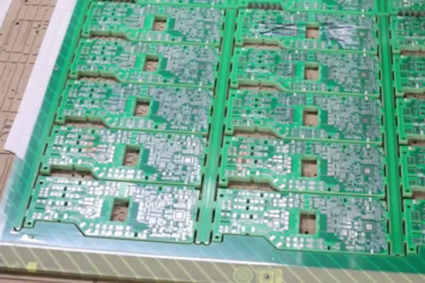
I’ve seen too many engineers oversimplify high multilayer PCB manufacturing. They always think that finding a factory with high-end equipment is enough. In reality, what truly determines success or failure is often those unseen details.
Take materials, for example. Many people believe that choosing high-end PCBs solves all their problems. However, even within the same batch, there can be subtle differences. We’ve encountered situations where the same roll of PCB showed subtle performance changes after being stored at different temperatures. These subtle differences might not be noticeable on a single-layer board, but in a stack of more than ten layers, they can trigger a domino effect.
Truly professional high-multilayer PCB manufacturing services establish their own material databases. They record the characteristic curves of each batch of materials. This isn’t just simple data recording; it’s about thoroughly understanding the material’s properties. For example, they track environmental data throughout the entire process from warehousing to production, even including temperature and humidity history during transportation. This data is then correlated with subsequent lamination parameters and drilling quality to build a predictive model of material behavior. When new materials arrive, engineers can predict their processing characteristics based on similar material curves in the database.
The issue of expansion and contraction is even more interesting. Some manufacturers prefer to remedy the situation afterward. For example, if they discover misalignment, they simply adjust the parameters. This approach is like shooting at a moving target without predicting its trajectory; instead, they wait until the bullet flies out and then manually push it. Professional manufacturers take proactive measures during the material pretreatment stage, such as pre-baking to eliminate internal stress or using a stepped heating and pressing process to allow each layer of material to deform synchronously. They even design differentiated compensation coefficients for core boards with different pattern densities, because uneven copper foil distribution can lead to localized stress differences.
The truly sophisticated approach is to reserve flexibility during the design phase. This includes using symmetrical laminated structures to balance stress, placing process edges to absorb deformation, and using highly flexible prepreg as a buffer layer. Some high-end designs even insert low-flow prepreg between critical layers to form mechanical anchors and inhibit interlayer slippage.
I particularly admire manufacturers who conduct stress testing. They are not satisfied with standard procedures but simulate various extreme conditions. For example, they deliberately subject the boards to temperature and humidity fluctuations before measuring the deformation. I have seen manufacturers build programmable environmental test chambers that can reproduce the temperature and humidity cycles from tropical oceans to deserts. They discovered that materials develop permanent dimensional memory after three humidity cycles, a finding that directly impacts warehouse management standards.
One visit to a factory left a deep impression on me. Their lamination workshop employs zoned temperature control, with materials of different thermal expansion coefficients pre-treated in different areas. Operators, like master chefs, precisely control the heat, adjusting pressure curves based on real-time monitoring of medium viscosity changes. More remarkably, they equip each lamination plate with micro-strain sensors, capable of capturing minute deformations undetectable by traditional methods.
The biggest pitfall in high-layer plywood manufacturing is making assumptions. For example, assuming all high-TG materials behave uniformly while ignoring the differences in rheological properties caused by different resin systems. We once observed a 0.3% difference in expansion and contraction between boards using the same model but different curing agent ratios, under the same lamination parameters. This error, amplified to a fatal misalignment in 20-layer plywood, is significant.
Good manufacturers treat every step as a dynamic process. They establish dynamic process windows rather than fixed parameters, such as adjusting vacuum lamination time based on the day’s atmospheric pressure. One factory’s engineer developed the habit of recording the temperature of everyone’s coffee during the morning meeting, saying it trains sensitivity to subtle changes—though seemingly a joke, this mindset is indeed reflected in their process control.
I remember a project that gave us a real headache. The boards had many layers and a large area, and the client demanded strict control over thickness tolerances. The conventional method was to measure and correct after lamination, but top manufacturers use real-time thickness compensation technology. They implant microwave probes inside the press to monitor resin flow, working in conjunction with an adaptive pressure system—it’s like having an autopilot installed in the lamination process. When excessive resin flow is detected in a certain area, the pressure is locally reduced to maintain uniform thickness.
Later, we discovered the key was understanding the material memory effect. For example, FR-4 material develops stress memory after the first high-temperature lamination; if the temperature exceeds the memory threshold during a second lamination, abnormal deformation will be triggered. Some manufacturers have developed a material “memory-erasing” process, using a specific temperature sequence to eliminate historical processing marks, allowing the multilayer board to maintain dimensional stability as if it were the first lamination.
Looking back now, most of those failures were due to details. For example, once, cleaning agent residue caused insufficient interlayer bonding, and a 0.1mm difference in tool wear caused fluctuations in drilling quality. The most alarming incident was that a batch failure stemmed from a new employee not wearing absorbent gloves as per regulations; moisture on their fingertips caused localized dampness when handling the core board.
Truly reliable manufacturers share a common trait: they don’t treat manufacturing as a routine process, but rather as an art requiring constant adjustment. Each batch presents a new challenge, demanding a renewed understanding of the material’s properties—this is the essence of high-quality multilayer PCB manufacturing. They respect material properties like a Michelin-starred chef treats ingredients, and focus on seamless process integration like a Swiss watchmaker treats a movement. This dynamic manufacturing philosophy is reflected in their always-open process manuals—every page filled with handwritten annotations, recording the new material characteristics discovered during the third shift the previous night.
I recently chatted with some friends who work in hardware development and noticed something interesting—many people prioritize price and technical specifications when choosing a high-multilayer PCB manufacturing services provider. This is certainly valid, but I always feel something is missing.
I remember a project we did last year that required a PCB board supporting 112G transmission. There were quite a few manufacturers on the market that could do it, but instead of rushing to compare prices, we spent time talking to several potential suppliers about their R&D strategies. One detail that impressed me was that the technical lead of one supplier proactively asked about our product plans for the next three to five years. He said that if they knew our development direction, they could adjust their production line processes in advance and even jointly develop new materials. This forward-thinking attitude is far more meaningful than simply offering a low price.
In fact, PCB manufacturing, especially high-multilayer boards, is no longer a simple OEM relationship. Good suppliers treat you as a partner on the technical journey. For example, during the debugging phase, we discovered a slight crosstalk issue on a certain signal layer. The factory we were working with immediately sent engineers with testing equipment to our lab overnight. They stayed there for two days and finally discovered that it was due to a mismatch in the thermal expansion coefficients of the materials. They went back and immediately adjusted the lamination process. This kind of tacit understanding of solving problems together cannot be cultivated in short-term cooperation.
I’ve seen too many teams save a few percent of costs by switching suppliers, only to lose more time and resources during mass production due to fluctuating yield rates. Currently, there are only a handful of manufacturers in the industry capable of producing 112G high-end PCBs, but perhaps only one or two are truly willing to commit to tackling the most challenging aspects together. During a recent visit to a factory we’ve been working with for a long time, we discovered they’d dedicated a high-precision back-drilling production line specifically for our product line. This kind of investment isn’t something a contract can guarantee; it’s built on the foundation of jointly overcoming several technical hurdles.
Some might think that getting too close to suppliers will diminish their bargaining power. Actually, the opposite is true. When we make our annual procurement volume transparent, they’re more willing to invest in equipment upgrades—after all, stable orders have more long-term value than scattered high-profit projects. Last year, they proactively suggested we optimize some layers from 18 to 16 using new dielectric materials, which resulted in better signal integrity. The cost optimization brought about by this deep collaboration is far more effective than simply haggling.
Choosing a PCB supplier is like finding a mountain climbing partner. Just looking at who has the lowest equipment and price isn’t enough; you need someone willing to climb the mountain in the dark with you and watch the sunrise together.
I’ve seen too many engineers oversimplify High Multilayer PCB manufacturing services. They always think that as long as the design is beautiful, a good circuit board can be made—but the real challenges lie in the unseen details.
Take electroplating, for example—it’s not just about putting a copper jacket on the board and calling it a day! Once, we tested a sample from a certain factory—the surface looked bright and smooth—but upon cross-sectioning, the copper in the center of the holes was as thin as paper—such a board would definitely have problems after three months—the requirements for electroplating processes with high aspect ratio through-holes are incredibly demanding—ordinary DC electroplating simply can’t penetrate—pulse electroplating with special chemicals is necessary—and every parameter must be controlled like mixing a cocktail. Temperature fluctuations in the electroplating solution exceeding plus or minus two degrees Celsius will affect the activity of copper ions, and the stirring speed determines the chemical exchange efficiency. Some manufacturers reuse filtered waste liquid to save costs, leading to the accumulation of organic impurities and the formation of a loose plating structure. More importantly, what appears to be a perfect hole wall under backlight testing will exhibit copper ion migration under high temperature and humidity conditions, forming micro-short circuits.
Drilling is an even more interesting topic—many people think it’s just about making a hole—but choosing the right drill bit is far more complex than imagined. I’ve seen manufacturers, in an effort to save costs, use a drill bit to its last possible lifespan, resulting in holes with walls so rough they could be used as sandpaper—making it impossible for subsequent electroplating to adhere. This causes the board to overheat during operation, leading to the copper layer peeling off directly from the hole, and the entire system collapsing. Different substrate materials require drill bits with specific coatings; for example, processing boards containing ceramic fillers requires diamond-coated drill bits. Matching the feed rate and spindle speed is also a science; too fast will cause thermal stress cracks, while too slow will create burrs. Modern advanced drilling machines are also equipped with laser positioning systems that automatically compensate for hole position deviations caused by thermal expansion and contraction of the material.
What truly impresses me is the attention to detail I witnessed during a factory visit—their drilling machines could monitor drill bit wear in real time—the automatic tool change time was accurate to the minute—this dedication to detail is key to producing high-layer PCBs. Every 500 holes machined, an optical probe scans the drill tip geometry, while spindle current changes are monitored to determine the wear condition of the cutting edge. This preventative maintenance, while increasing tooling costs, avoids loss of positioning accuracy due to excessive drill wear, which is crucial, especially for machining micro-holes smaller than 0.2mm.
However, the most easily overlooked step is lamination—many people think it’s simply pressing several layers of material together—but it’s far more complex. Even slight differences in temperature profiles or uneven pressure distribution can create invisible gaps between layers. These tiny gaps expand with temperature changes, eventually causing the entire board to delaminate and become unusable. The pre-baking process before lamination is often neglected; in fact, if volatiles in the prepreg are not completely removed, they will form gas channels during high-temperature pressing. Modern presses use zoned temperature control technology, setting different pressure gradients for the edges and center of the board, and adjusting the holding time in real time according to the material thickness.
I remember a client insisting on using hybrid materials for their 16-layer PCB—laminating high-speed materials with standard FR4 was as difficult as mixing oil and water. We adjusted the heating profile to perfectly match the flow rates of the different materials, resulting in a finished product so flawless that even ultrasonic scanning couldn’t detect a single air bubble. Specifically, we controlled the heating rate at 1.5℃/minute within the 80-120℃ range, allowing the low-Tg materials to soften and flow first, then simultaneously curing them once they reached their glass transition temperature. We also added a special buffer film between each layer to absorb the differences in thermal expansion coefficients between the different materials.
Ultimately, making high-multilayer PCBs is like cooking a delicate dish—every step must be just right—cutting corners in any step will affect the final quality. Now, I skip manufacturers who only offer low prices without discussing the manufacturing process—after all, PCBs are used in actual products—poor quality damages the reputation of the entire project.
I’ve seen too many companies stumble when choosing high-multilayer PCB suppliers. They are often attracted by the initial price but ignore the true technical hurdles. Once, our company was preparing to build a 32-layer communication pcb and received quotes from five suppliers. The cheapest one confidently claimed they could do it, but the sample showed serious interlayer alignment problems. It turned out their equipment simply couldn’t handle the precision requirements of this type of stack-up. This experience taught me that the manufacturing capability of high-multilayer boards cannot be measured solely by price.
The real test of a supplier’s competence lies in their control of CAF (Compact Aspect-Oriented Flame) issues. I once worked with a customer who manufactured industrial control equipment; their products needed to operate for extended periods in high-temperature and high-humidity environments. The initial supplier they chose, while having a price advantage, exhibited CAF during accelerated aging testing, necessitating a complete redesign of the entire batch. They later switched to a supplier with a comprehensive CAF prevention system; although the unit price was 15% higher, they saved on rework costs. These hidden costs are often overlooked in the early stages of a project.
Now, when my team and I evaluate suppliers, we pay particular attention to their stack-up design capabilities. Good suppliers can recommend appropriate lamination schemes based on the product’s application scenario, such as when to use mixed dielectric materials and how to arrange the order of signal and power layers. These details may seem minor, but they directly impact the reliability of the final product. Once, an engineer from a medical device motherboard supplier suggested adjusting the ground plane layout. This change improved signal integrity by 20%.
Global delivery capabilities are also a crucial consideration. Last year, we had a project requiring the simultaneous production of the same 28-layer PCB in North America and Asia. Our supplier had factories in both China and Malaysia, which allowed us to successfully mitigate supply chain risks caused by lockdowns in certain regions due to the pandemic. They could even provide complete production records in both Chinese and English—a detail particularly critical for products requiring international certification.
In reality, selecting a high-layer-count PCB manufacturer is much like finding a business partner. In the short term, the focus may be on price; however, over the long term, technical capability and service reliability are the true priorities. Nowadays, I prefer to select suppliers who proactively offer technical recommendations—even if their quotes are not the lowest. This is because their focus extends beyond simply securing an order; they are dedicated to ensuring the product genuinely meets its design specifications.
I recently chatted with some friends who work in hardware design and noticed a rather interesting phenomenon. These days, when people talk about high-multilayer PCB manufacturing, they tend to focus on fancy technical terms like glass substrates and optical interconnects. But honestly, the key to whether a board can last three to five years stably often lies in the most basic process details.
Take material expansion and contraction, for example. Many manufacturers like to advertise how advanced their compensation algorithms are. But we’ve actually encountered situations where boards made from the same batch of materials in different seasons can differ in size by half a millimeter. We later discovered that their warehouse temperature control wasn’t done well; the epoxy resin already carried internal stress when it arrived at the warehouse. Even the most sophisticated AI prediction models can’t calculate this kind of problem; experienced craftsmen have to feel the subtle deformation by touching the edges of the boards.
Speaking of the lamination process for multilayer boards, a factory visit I recently visited left a particularly strong impression. Their showroom’s sample cabinets displayed various gleaming back-drilled cross-section diagrams of sample boards—it was quite impressive. But when I went to the production workshop, I noticed a detail—the operators would blow the holes on the worktable with an air gun more than three times before stacking the boards. Their movements were incredibly practiced and fluid, almost like muscle memory. This zero-tolerance attitude towards dust is more effective than any testing equipment.
Some high-multilayer PCB manufacturing services love to emphasize how advanced their equipment is, but we value more how they handle abnormal situations. Once, a supplier delivered a batch of boards with minor interlayer misalignment. Their engineers stayed on-site for three days with microscopes, repeatedly comparing the operation videos of each process. They finally discovered that the problem stemmed from a problem with the venting rhythm during hot pressing. This ability to trace the root cause is true competitiveness.
Actually, there’s a simple way to judge a supplier’s reliability: see how they treat scrap. I’ve seen a factory that categorizes scrap boards by process, stacking them like library archives, even attaching a defect analysis report to each scrap board. This attitude of treating failure as a lesson is more convincing than constantly boasting about success rates.
Ultimately, high-end manufacturing boils down to a battle of fundamental skills. Just like building a house, no matter how fancy the facade, a solid foundation is key.
I recently chatted with a friend who works in the telecommunications equipment industry and noticed something interesting. His company was running into a lot of trouble finding suppliers capable of handling PCBs with 30 or more layers for a new project – the manufacturers who usually boasted about their capabilities suddenly fell silent. This reminded me of a mistake I made last year: I thought I had found a reliable multilayer PCB manufacturer, and the sample tests went smoothly, but during mass production, the entire batch of boards developed delamination issues.
Many people have a misconception about high-multilayer PCBs, thinking it’s simply a matter of adding more layers. The real test is maintaining stable bonding between dozens of copper foil layers under different temperature conditions. I once visited a long-established factory where their lamination workshop maintained constant temperature and humidity year-round, and even employee entry and exit had strict procedures – these details are key to ensuring quality.
Many manufacturers on the market claiming to provide high-multilayer PCB manufacturing services haven’t even mastered the basic multilayer PCB processes. For example, a client brought us a supposedly 40-layer design for evaluation, and upon opening the files, we saw that the blind and buried via designs were completely illogical. Truly professional multilayer PCB manufacturers intervene during the design phase, pointing out which traces need optimization and which layers require additional shielding.
I particularly dislike the way some manufacturers mystify high-layer PCBs. All that talk of exclusive formulas and cutting-edge technology ultimately comes down to fundamental skills. I once saw two factories using the same model of press: one produced a 56-layer board that passed military-standard testing, while the other frequently warped even with a 20-layer board. The difference lay in their depth of understanding of material properties.
Regarding factory selection experience, I don’t think it’s necessary to be too fixated on the age of the equipment. I once saw a small factory in Dongguan using secondhand equipment, but the experienced workers had calibrated the parameters more precisely than some large automated factories. Their secret to multilayer PCBs was adding a 24-hour natural cooling cycle after each lamination. Although this slowed down delivery times, the yield was remarkably stable.
Currently, there’s a strange cycle in the industry where everyone blindly pursues a multilayer race while ignoring actual application scenarios. In most cases, around 20 layers is sufficient for 90% of high-speed signal requirements; the key is to ensure proper impedance control and heat dissipation design. The most successful case I’ve handled was actually an 18-layer server motherboard, because every detail was meticulously refined.
If you’re considering a high-multilayer PCB project, my advice is to first clarify your actual needs. Don’t be misled by fancy layer count claims; focus on the factory’s understanding of material compatibility and whether they’ve handled similar complex cases. Sometimes, choosing a mid-sized but highly focused supplier is safer than chasing after large manufacturers.
Having worked with high-multilayer PCBs for so many years, I’ve increasingly realized that finding the right supplier is more important than obsessing over technical parameters. Some problems that appear to be process defects actually stem from the supplier selection.
Take the CAF (Compatibility and Adhesion) issue, for example. I’ve seen too many people only think about checking materials after equipment malfunctions. In fact, you should pay attention to whether a supplier has comprehensive CAF testing capabilities from the very beginning. Some small factories, to save costs, use ordinary FR4 material for high-speed boards with insufficient insulation thickness. Boards that test fine when they leave the factory start leaking current after a year or two.
I particularly value the transparency of a supplier’s production data. Good manufacturers will proactively show you the interlayer alignment reports for each batch of boards, instead of providing data to explain problems only after they arise. Once, we had a project where a back-drilling depth deviation caused signal problems. We later discovered that the supplier’s online monitoring records were simply for show. Since then, I’ve been willing to spend more money to find partners who can share production data in real time.
In fact, the biggest fear in high-multilayer PCB manufacturing is situations where things appear fine on the surface but harbor hidden problems. Defects like insufficient copper thickness in the core are impossible to detect in routine spot checks. They only become apparent during high-temperature testing of the entire machine at the customer’s site, resulting in batch defects. The loss isn’t just money, but also the customer’s trust.
Now, when I negotiate with suppliers, I always include specific requirements for CAF (Constant Failure Mode) prevention in the contract. After all, this type of failure mode might not manifest for one or two years, making it difficult to assign responsibility then. Good suppliers understand this concern and may even proactively suggest using more reliable material solutions.
Regarding warpage, I think the key isn’t in the acceptance criteria but in stress control during the production process. Experienced manufacturers will perform specialized stress relief treatment after lamination instead of simply relying on baking. After switching to a supplier that focuses on process control, our SMT assembly yield increased by more than ten percent.
I’ve learned my lesson the hard way about delivery delays. I later discovered that instead of rushing the process, it’s more important to assess the supplier’s actual capacity beforehand. This is especially true when using special materials; you need to see if they have stable procurement channels. Now, I have suppliers include material procurement cycles in their production schedules, which significantly reduces the need for emergency rush orders.
Ultimately, the quality of high-multilayer PCBs isn’t determined by final acceptance testing, but rather by the selection of suppliers. Instead of getting bogged down in specific parameters, it’s better to invest time in finding partners who truly understand the process.
Making high-multilayer PCBs sometimes feels like walking a tightrope. I’ve seen too many manufacturers claiming to provide high-multilayer PCB manufacturing services; they all confidently guarantee no problems during the sample stage, but their shortcomings are exposed once mass production begins.
I remember once during a factory audit, their lab’s electroplating parameters were set extremely aggressively, supposedly to shorten the production cycle. The first batch of goods failed the thermal cycling test; cross-sections revealed that the copper thickness in the vias was less than 20 micrometers. No matter how good the surface work looks, the true colors are revealed once actual production accelerates.
When choosing suppliers now, I value their adaptability more. Once, a partner needed to adjust the laminate structure at the last minute, and their engineers recalculated all the parameters that very night, even resimulating the lamination temperature profile more than twenty times. This dedication to detail is true skill, far superior to those who simply follow the book blindly.
Actually, there’s a simple way to judge a manufacturer’s competence—observe how they handle unexpected situations. Last time, the production line suddenly lost power, and one factory managed to manually record the electroplating time of each board down to the second. In the end, the uniformity of the copper in the holes in that batch was even better than usual.
Ultimately, the biggest pitfall in high-layer PCB manufacturing is rigid, formulaic operations. Some manufacturers are so inflexible with their processes that they can’t operate if they change materials or thicknesses. A truly reliable supplier should be like a skilled traditional Chinese medicine practitioner taking a pulse, dynamically adjusting parameters based on the characteristics of each batch of materials.
A recent project I’ve been working on clearly illustrates this. Both are making 20-layer boards, but some manufacturers can’t seem to get impedance control right, while others can control even the back-drilling step within 0.05 millimeters. The difference isn’t determined by equipment; it’s entirely a matter of the engineer’s depth of understanding of the process.
The most impressive example I’ve seen is a trial production where, after discovering slight variations in batches of boards, the manufacturer proactively adjusted the temperature gradient of the electroplating bath three times. Ultimately, the thermal reliability of this batch of boards exceeded design standards. This ability to adapt flexibly is the key difference between ordinary factories and top-tier suppliers.
Now, when I encounter new suppliers, I rarely ask how many layers they can produce; I’m more concerned with which process parameters they’ve improved in the last three months. Manufacturers who are meticulous about details are more reliable when producing high-multilayer PCBs.
I’ve seen too many teams stumble in high-multilayer PCB design. Sometimes, even with an ingenious circuit design, a lack of attention to manufacturing details can derail the entire project. Especially when it comes to high-multilayer PCB manufacturing services, many people overlook a crucial issue—the compatibility between materials.
Once, our team was making a 16-layer board, using a mixture of two different substrate types. Under high temperatures, the difference in the expansion and contraction rates of the two materials caused minor misalignments in the inner layer circuitry. Although the error is only a few tens of micrometers, it’s disastrous for high-frequency signals. This experience made me realize that simply looking at the parameter tables of individual materials is far from enough; the interactions between materials in actual applications must be considered.
CAF (Copper Acid Migration) is an even more insidious killer. I remember a client’s product testing perfectly in the lab, but two years after being released to the market, it began to experience inexplicable malfunctions. Disassembly and analysis revealed that copper ion migration had occurred between adjacent vias. This problem could actually be avoided at the manufacturing stage, such as by using CAF-resistant materials or optimizing the drilling process. Unfortunately, most people only regret it after the problem has surfaced.
Now, when faced with complex projects, I pay special attention to the manufacturer’s understanding of material properties. Excellent suppliers build their own material databases and simulate expansion and contraction in advance for different stacking schemes. They can even dynamically adjust compensation parameters based on batch differences in the boards—this is truly valuable service.
Ultimately, the reliability of high-layer plywood isn’t achieved through some magical process, but rather stems from meticulous attention to every detail. Like building blocks, the flatness of each layer affects the stability of the overall structure. Sometimes, the most inconspicuous material properties can become the key factors determining success or failure.
I’ve seen too many companies make the same mistake when choosing high-multilayer PCB manufacturing services—they treat suppliers like temporary workers. They switch to one supplier today because of the lower price, and jump ship to another tomorrow because of faster delivery. This constant switching results in stagnant quality. This frequent changeover often leads to suppliers lacking in-depth understanding of the company’s technical expertise and specific needs. Each collaboration requires re-adjustment, increasing communication costs and trial-and-error risks. For example, in critical processes like impedance control or material compatibility, new suppliers need time to adapt to the company’s specific standards, which can easily cause stability issues during mass production.
Truly reliable partnerships require you to invest time in in-depth research. Last year, when we visited a seemingly ordinary supplier, we discovered a detail: their engineers could accurately recall impedance deviation data from a project we had three years ago. This kind of memory cannot be developed through last-minute cramming. This reflects that the supplier has established a comprehensive customer profile system, using digital tools to track key parameters for each project and quickly accessing historical data to aid decision-making. For example, they might use a PDM system to manage design changes or a MES system to record anomalies during production, thus creating a traceable knowledge base.
An interesting phenomenon is that many people treat audits like exams. They rush through the equipment parameters with a checklist and think they’ve completed their task. In reality, you should sit down and chat with the technical director, asking about recent process challenges and observing their team’s problem-solving approaches—this is far more valuable than simply requesting test reports. For instance, you can observe how they handle drilling burrs on high-frequency boards or how they optimize the lamination process to reduce layer misalignment. These real-world examples reveal the supplier’s true technical capabilities, such as whether they possess DOE experimental design capabilities or can continuously improve process windows through CPK analysis.
I particularly dislike suppliers who use technical parameters as bargaining chips. I once encountered a factory that required multiple layers of approval to access SPC data; we later discovered they couldn’t even achieve basic process traceability. Conversely, the company we’re currently working with proactively shares real-time production line data with us and even invites us to participate in their quality improvement meetings. This transparent operation is reflected in specific details. For example, they use a QMS system to automatically generate quality reports or share DFM analysis reports during the NPI stage. Even more valuable is their regular cross-plant technical seminars, where they collaborate to tackle common problems such as insufficient blind and buried via filling.
The most tangible benefit of long-term cooperation is shared risk. Last quarter, when raw material prices fluctuated, our suppliers notified us two weeks in advance to adjust material plans and shared some of the cost increase pressure. This tacit understanding cannot be bound by a mere contract. This deep collaboration is also reflected in capacity planning. For instance, suppliers will stockpile special materials in advance based on our forecasts or reserve flexible capacity for urgent orders. When a sudden quality issue of micro-short circuits occurred on HDI boards, they could quickly initiate the 8D reporting process and form a joint team with us to analyze the root cause overnight.
In fact, there’s a simple standard for judging whether a supplier is worth deep cooperation: see if they are willing to expose their weaknesses. Those who dare to proactively discuss process bottlenecks are often more trustworthy than those who only boast about their equipment. After all, PCB manufacturing is inherently a process of continuous problem-solving. For example, some suppliers frankly admit that their immersion gold process still needs improvement in terms of uniformity of hole wall coverage for aspect ratios greater than 8:1, and demonstrate their pulse electroplating solution under testing. This technical honesty is reassuring because it shows they have established a mechanism for continuous improvement.
Such a professional attitude often helps us avoid numerous pitfalls during the later stages of a project. We recently experimented with involving our suppliers early in the new product design process, and the results were unexpectedly positive. Based on their manufacturing expertise, they proposed optimizations to our PCB stack-up that directly boosted our production yield by five percentage points. This kind of technical feedback—flowing from the manufacturing end back into the design process—represents the core value of a strategic partnership. Specifically, during the design phase, they identified a risk of resin residue accumulation in the overlap zones between blind and buried vias within our original layout. They subsequently recommended adjusting the dielectric layer thickness and switching to low-flow prepreg materials. This type of input, grounded in practical manufacturing experience, also proved instrumental in optimizing our thermal via layout and impedance matching structures.
Ultimately, choosing a High Multilayer PCB supplier is like finding a business partner. Looking at hardware configurations alone is far from enough; what’s more important is the alignment of values and the willingness to grow together. Truly excellent cooperation is reflected in the daily details. For example, the supplier’s project manager will proactively share new industry technologies or coordinate alternative production capacity in advance during equipment maintenance periods. Once both parties establish a technical language framework, even engineering changes can be quickly confirmed through video conferences—an efficiency improvement that short-term cooperation cannot match.
I’ve always found working with high multilayer PCBs quite interesting. Many people think that finding a supplier who can take orders is enough. But what truly tests a supplier’s ability to grasp every aspect of the process is crucial. I remember once when we were making boards for communication base stations, we were going to the factory every day.
That’s when we realized that, even in the testing phase, some manufacturers just went through the motions, while others thoroughly understood every piece of data. An engineer showed me their records, which clearly documented even the minute changes in different batches of boards under high temperatures. This habit of in-depth analysis truly avoids many later problems.
Many manufacturers now claim to provide high-multilayer PCB manufacturing services, but few truly dedicate themselves to controlling the details. For example, regarding post-drilling treatment, some factories think a slightly rough hole wall is fine, but in reality, it directly affects signal transmission quality. The most meticulous suppliers I’ve seen meticulously record the lifespan of each drill bit and replace worn parts in advance.
When choosing suppliers, I particularly value their attitude towards problems. Once, a batch of boards exhibited slight impedance fluctuations during testing, and the supplier immediately halted production and spent two days investigating, discovering it was a temperature control deviation in the lamination process. Although it delayed delivery, this responsible approach gave me greater peace of mind.
In fact, manufacturing high-multilayer boards is like assembling building blocks; the coordination between each layer is crucial. Sometimes, suppliers skip certain testing steps to meet deadlines. While the problems may not be immediately apparent, they compromise long-term stability. Good manufacturing services should be like a skilled traditional Chinese medicine doctor diagnosing a patient—seeing both the surface symptoms and understanding the underlying causes.
A recent project I worked on made this even more profound. During the design phase, I involved the supplier in discussions. Based on their manufacturing experience, they suggested adjusting the positions of two grounding layers, resulting in a 30% increase in the first-pass yield. This collaborative model of working backward from the manufacturing stage to design truly avoids many pitfalls.
Ultimately, finding a supplier isn’t about who offers the lowest price, but about who truly understands the manufacturing logic of high-multilayer PCBs. Manufacturers willing to invest time in in-depth process research often bring unexpected surprises.
I recently chatted with a friend who does hardware design and noticed an interesting phenomenon—many people, when they hear “High Multilayer PCB manufacturing services,” instinctively count the number of layers. It’s as if a 20-layer board is superior to a 16-layer one. This is actually quite interesting.
I remember a project we did last year where, when the board reached 20 layers, we suddenly discovered a signal integrity problem. Our first reaction was to add a shielding layer or adjust the stack-up structure, but after much trial and error, we realized it was due to inaccurate calculations of material expansion and contraction at different temperatures. A thin sheet of board can experience temperature differences exceeding 200 degrees Celsius across different processing stages.
That’s when you realize—increasing the number of layers isn’t a linear, incremental challenge. Each additional lamination of the substrate is like building with blocks; if the bottom is slightly off, the top will be completely tilted.
What truly changed my perspective was a visit to a professional factory. The most striking feature in their workshop wasn’t the automatic chip mounters, but their constant temperature and humidity system. An experienced worker pointed to the temperature and humidity curves on the wall and told me that the precision of high-layer boards is actually derived from environmental stability. Once, they received a 36-layer order, and they spent three days adjusting the lamination parameters just to accommodate material expansion and contraction.
Later, when we made 24-layer boards ourselves, we learned our lesson—we stopped obsessing over the number of layers and instead focused on thoroughly understanding the temperature drift characteristics of the board. We discovered that changing the fiberglass cloth could reduce the Z-axis expansion coefficient by one-third.
Now, when I see manufacturers advertising “30+ layer boards,” I always ask: How do you control the cumulative error after multiple laminations? The answer is often more interesting than the number of layers itself. Sometimes they’ll start talking about X-ray drilling compensation technology, and sometimes they’ll present comparative data on the expansion and contraction of different materials—these are the things that truly demonstrate manufacturing prowess.
Ultimately, the complexity of a PCB is never determined by the number of layers alone. Just like building a house isn’t just about the number of floors, but also the stability of the foundation. Next time someone boasts about the specifications of a 50-layer board, ask them how they solved the problem of plating uniformity when the aspect ratio exceeds 15:1—the answer to this question often speaks volumes about their manufacturing capabilities.
By the way, never blindly trust the standard expansion and contraction coefficients provided by manufacturers. Even core boards of the same model will have slight differences between different batches; it’s best to perform pressure testing on each batch. We learned this the hard way and developed the habit of cutting small samples and running them through three thermal cycles before making any decisions.
When choosing a reliable High Multilayer PCB manufacturing services supplier, I think you can’t just look at how many imported machines are in their workshop. Those gleaming machines can certainly impress for a while—I was once dazzled by a wall of imported drilling rigs during a factory visit—but what truly determines product stability is often what’s unseen.
For example, the issue of board expansion and contraction is particularly challenging and requires accumulated experience. Once, we urgently needed to find a new supplier to produce samples of 20-layer boards. They confidently guaranteed accuracy within 0.3%, but upon receiving the goods, we found that all the positioning holes were offset by half a millimeter. Later, after reviewing their process records, we discovered that although the factory had new equipment, they used a fixed compensation value for every different thickness of laminate. This rigid approach was passable for 8-layer boards, but disastrous for higher-layer boards.
Now, when we audit, we focus on their data flow logic. Truly professional suppliers will proactively display historical order expansion and contraction fluctuation curves and even explain the impact coefficients of different copper thickness combinations on dimensions. I remember an engineer from a factory in southern China directly pulled up a scatter plot of compensation values for all high-layer boards over the past three months on the screen. This data-driven approach is much more reassuring than simply boasting about equipment parameters.
There’s actually a clever way to test a supplier’s capabilities: deliberately present them with an unconventional multilayer PCB solution to gauge their reaction. Last time, we designed a hybrid multilayer PCB structure and visited three potential suppliers with the blueprints. The first repeatedly emphasized the need for a 30% special process fee; the second’s sales manager readily agreed but couldn’t explain the specific control measures; and the third’s technical director immediately drew a stress calculation sketch. Ultimately, we chose the third supplier, even though their price wasn’t the lowest, because their initial trial production yield reached 92%.
Finally, finding a high-multilayer PCB supplier is like choosing a marriage partner—it’s not about the dowry, but about their problem-solving abilities. Factories that treasure the testing data from each stage are often more trustworthy in the long run than those that only display machine labels.
While collaborating with a smart wearables team to select a semiconductor flex
We often regard electronic products as a glossy whole, but ignore the
Many assume that choosing China for PCB assembly is solely about saving
• Expert in Small-to-Medium Batch Production
• High-Precision PCB Fabrication & Automated Assembly
• Reliable Partner for OEM/ODM Electronic Projects
Business Hours: (Mon-Sat) From 9:00 To 18:30