
How Do PCBs for Medical Devices Hold the “Last Line of Defense for Life”?
In the field of medical electronics, attention often focuses on complex algorithms;
I’ve always found the subject of heat dissipation in electronic devices quite fascinating. Back when I used to disassemble old computers, I noticed numerous small copper plates embedded beneath the chips on the motherboard—I later learned that this is known as “Copper Coin PCB” technology. However, many people tend to overlook a crucial detail: the true power of the “copper coin” lies not merely in the material’s inherent ability to conduct heat quickly.
I once conducted a comparative test while helping a friend upgrade their graphics card cooling system. I attached aluminum and copper plates of identical dimensions to the back of the GPU; after running a video game for half an hour, the temperature difference was striking. The aluminum plate became so scorching hot that I couldn’t even touch it, whereas the copper plate remained cool enough to hold my hand against for several seconds. This reminded me of my childhood winters: if I grabbed an iron railing, my hand would feel as though it were sticking to the metal, but grabbing a wooden stick posed no such issue—metal conducts heat so rapidly that it instantly draws the thermal energy away.
Nowadays, to cut costs, some manufacturers use copper-plated aluminum plates to pass off as solid copper structures. While they may look metallic on the surface, their actual performance falls far short. It is much like buying a thermal flask: the thickness of the stainless steel inner liner makes a world of difference in how well it retains heat. What truly determines cooling efficiency is whether the thermal conduction path is continuous and unobstructed.
The most impressive design I’ve ever encountered involved extending the copper coin directly to the metal support frame of the device casing. The heat seemed to slide effortlessly—almost as if down a chute—from the chip all the way out of the chassis. This even allowed the fan speeds to be reduced—an integrated design philosophy that is far more compelling than simply “stacking materials” (over-engineering with brute force components). In fact, nature has long possessed a similar form of ingenuity: the hollow structure of polar bear fur not only retains heat but also efficiently dissipates excess body heat. Artificial thermal management designs should likewise draw inspiration from this bidirectional approach to heat regulation, rather than blindly chasing after isolated performance metrics.
While recently researching thermal management issues in circuit boards, I stumbled upon a rather intriguing phenomenon. Nowadays, whenever high-performance cooling is mentioned, many people immediately think of utilizing copper-clad substrates or attaching external heat sinks. However, a far more elegant solution lies hidden within the details: the “copper coin” embedding technique. Although seemingly simple, this design achieves astonishing thermal management results within a limited spatial envelope. The core principle of this technique involves embedding miniature copper thermal conductors directly into the insulating substrate of a PCB, utilizing precise placement to establish highly efficient thermal conduction pathways. For instance, by densely embedding copper coins directly beneath a processor or power chip, these elements act like miniature heat pipes, rapidly spreading heat laterally from localized hotspots across the entire surface of the board, thereby preventing the formation of dangerously high-temperature zones.
I recall once disassembling a piece of vintage industrial equipment and discovering that its PCB actually employed a structure akin to this “copper coin” design. Dozens of tiny copper pillars—each less than two millimeters in diameter—were neatly embedded within the board; when I touched the surface, I could distinctly feel the heat being rapidly drawn away. The true brilliance of this design lies in the fact that, unlike external heat sinks, it consumes no additional physical space. It is particularly well-suited for portable devices with compact internal layouts, or for applications requiring hermetically sealed enclosures, as the embedded design preserves the flatness of the board surface and requires no additional mechanical fasteners.
Currently, some engineers still harbor misconceptions regarding copper-coin PCBs. Some assume they are applicable only to high-power scenarios. In reality, however, even minuscule copper coins can play a pivotal role in temperature-sensitive applications—such as medical devices. I once examined the circuit board of a cardiac pacemaker; embedded within it were dozens of sesame-seed-sized copper dots that simultaneously ensured effective heat dissipation and minimized overall weight. These copper dots were not distributed uniformly; instead, their placement was strategically optimized based on thermal imaging data of the chips—for instance, appearing in higher density around the RF module and power management IC—thereby effectively maintaining the operating temperature within a safe threshold.
When selecting this type of circuit board material, one must not rely solely on published specifications. Some manufacturers may list impressive figures regarding the thickness of the embedded copper elements; however, it is often only after actual installation that one discovers a critical mismatch in the coefficients of thermal expansion. I once tested samples from a certain brand; their performance was excellent at room temperature, but as soon as the temperature rose, delamination began to occur. This happens because copper and the FR-4 substrate expand at different rates when heated. If the embedding process is flawed, cyclic thermal stress can cause micro-cracks to form between the copper coins and the substrate, thereby compromising long-term reliability. Superior manufacturing processes employ transition layer materials or specialized anchoring structures to mitigate this issue.
A truly effective copper-coin PCB should fit its application as comfortably and naturally as a well-worn pair of shoes. It does not require exaggerated thermal specifications, but rather the ability to maintain stability across a wide range of operating conditions. I particularly admire manufacturers who engage in targeted optimization. They adjust the density and distribution of the copper coins based on the client’s actual operating environment. For instance, to handle the high transient currents associated with cold starts in automotive electronics, they might increase the aspect ratio of the copper coins to boost instantaneous thermal capacity; conversely, for consumer electronics that undergo long-term, moderate operation, they might utilize a finer, denser array to ensure balanced heat dissipation.
A friend of mine in the automotive electronics sector recently shared a grievance with me. After switching to a new supplier, their product yield rate plummeted. It was later discovered that the new manufacturer’s surface treatment for the copper coins was substandard. Although the inspection reports appeared flawless, actual soldering operations consistently resulted in cold joints. The root cause lay in the fact that the microscopic oxide layer on the surface of the copper coins had not been thoroughly removed, leading to poor solder wettability. Such defects are difficult to detect through standard spot checks but inevitably surface during mass production.
This incident reminded me that one cannot judge the reliability of a copper-coin PCB solely by its certification certificates. Instead, one must evaluate the manufacturer’s level of attention to detail. For example, do they possess the experience to tailor their embedding process to different types of PCB substrates? Materials like Rogers laminates—commonly used in high-frequency circuits—differ significantly from standard FR-4 in terms of hardness and thermal properties. They require specific adjustments to stamping pressures and annealing protocols; otherwise, burrs may form along the edges of the copper coins, compromising signal integrity.
Sometimes, the simplest solutions are the ones that truly put a craftsman’s skill to the test. Much like ancient artisans crafting copper coins by hand, modern engineers designing these miniature copper coins require that same spirit of meticulous craftsmanship. They must holistically consider factors such as current load, heat source distribution, mechanical stress, and even electromagnetic compatibility; the diameter, spacing, and embedding depth of every single copper coin must be precisely calculated rather than merely copied from a standard template. Nowadays, I tend to favor suppliers who are willing to share case studies. They provide detailed explanations regarding the rationale behind the placement of every copper coin; this level of transparency often signifies a solid foundation of technical expertise. For instance, one supplier once presented a thermal simulation report for a drone flight control board; by adjusting the orientation of the diamond-patterned copper coins, they successfully reduced the motherboard’s peak temperature by 7 degrees Celsius while simultaneously avoiding interference with the GPS antenna located beneath it.
After all, no copper pad on a circuit board exists in isolation; each is inextricably linked to the thermal management strategy of the entire system. When deciding whether to implement this technology, one must weigh the options from the perspective of the product’s holistic design. If the product is expected to undergo frequent thermal cycling throughout its lifecycle, the fatigue resistance of the copper coin technology becomes a more critical factor than its sheer thermal conductivity; conversely, if the device is destined to operate in a high-vibration environment, one must carefully evaluate the impact of the copper coins on the board’s mechanical integrity. This holistic perspective is often far more valuable than merely chasing after a single performance metric.
I recall my first foray into copper coin PCB design, when a veteran engineer advised me not to overcomplicate the matter. Holding up a scrapped board, he pointed out tiny hairline cracks along the edges—fissures that resembled the parched, cracked earth of a dried-up riverbed. Such cracking typically occurs after exposure to extreme temperature fluctuations, particularly when the thermal expansion rates of the copper coins and the surrounding substrate materials are mismatched.
I later realized that the true key lies not in calculating parameters to the third decimal place, but rather in understanding how the various materials “interact” with one another. During one test, we intentionally used copper coins that were slightly thinner than recommended; under low-temperature conditions, the entire module actually warped slightly, much like a vinyl record. That lesson taught me that the selection of coin thickness cannot be based solely on theoretical values; one must also account for the extreme conditions that may arise during actual field operation.
Nowadays, when designing, I place a greater emphasis on overall harmony and coordination. For instance, I make a point of leaving a buffer zone around the copper coins—much like providing a dancer with ample stage space. While this approach does consume a bit of real estate on the board layout, it effectively mitigates the concentration of thermal stress. On one occasion, a client requested a board designed for use in a high-vibration environment; we deliberately shifted the placement of the copper coins 15% closer toward the center of the board. We later received feedback confirming that, even after 2,000 hours of continuous operation, the board exhibited absolutely no anomalies.
Most recently, while assisting a medical device manufacturer with product enhancements, I gained yet another fresh insight into this fascinating field. The client’s original boards began to delaminate after undergoing repeated high-temperature steam cycles in a sterilization cabinet. In response, we adjusted the substrate formulation and implemented a stepped “copper coin” embedding depth—much like designing distinct seismic-resistant structures for different floors of a building. After three months of accelerated aging tests, the insulation performance remained above 95% of its initial value.
In this line of work, the longer you stay in it, the more you realize that good design should resemble the intricate gear train of a vintage timepiece: every component retains its unique characteristics while operating in perfect harmony with the whole. During a recent factory visit to oversee mass production, I observed a veteran technician on the assembly line using a flashlight to cast a glancing beam across the boards, checking for uniformity in the copper coins’ reflectivity. Surprisingly, this simple, low-tech quality control method proved effective at detecting tiny air bubbles that often elude automated inspection equipment.
It is often fascinating to examine PCB samples from different eras. Military-grade boards from the 1990s, for instance, typically featured massive copper coins that were directly riveted into place; in contrast, modern consumer electronics tend toward a distributed layout featuring numerous smaller copper inserts. This evolution is fundamentally driven by the specific application environments, which compel technology to become increasingly refined. For example, during a recent automotive electronics project, we discovered that boards situated within the engine bay must simultaneously withstand two extreme conditions: the intense cold of a “cold start” and the scorching heat of prolonged idling. In such scenarios, relying solely on material selection is simply no longer sufficient.
It is my habit to retain a few sample boards from every completed project for long-term monitoring; some of these have been in operation for five or six years, and we continue to collect data from them. These boards—bearing the authentic marks of real-world usage—are far more compelling than any theoretical model. Every trace of oxidation or subtle discoloration on their surfaces tells a unique story of survival within a genuine operating environment.
I have long felt that many people today hold a somewhat skewed perception of high-performance hardware. People tend to fixate solely on chip model numbers while overlooking the fact that system stability is often ultimately determined by those unassuming, fundamental materials. Take “copper coin” PCBs, for instance: they may appear simple on the surface, yet they exert a profound influence on the actual performance of semiconductor devices.
I recall an instance last year while debugging a high-power device where we cycled through three different substrate materials. The first two were standard, off-the-shelf options, yet neither managed to achieve the required thermal dissipation. We then decided to replace the conventional copper cladding with a “copper coin” structure—and the temperature immediately dropped by over ten degrees Celsius. This level of improvement cannot be achieved merely by swapping out a heatsink; it fundamentally alters the entire thermal conduction pathway.
As semiconductor devices become increasingly sophisticated and miniaturized, the demands placed upon their thermal management systems continue to rise. Standard PCBs perform adequately under low-power conditions; however, once subjected to sustained high loads, the issue of heat accumulation becomes particularly pronounced. I have witnessed far too many instances of performance instability caused by insufficient heat dissipation—situations where the chip itself possessed ample capability, yet its potential was held back by the limitations of the underlying substrate materials.
The technique of embedding “copper coins” is actually quite ingenious. Unlike external heat sinks, which serve merely as passive after-the-fact remedies, this approach integrates thermal management directly into the circuit design itself. This shift in mindset is crucial; it signifies that we must factor in heat dissipation right from the initial stages of design, rather than attempting to patch things up retroactively. Nowadays, whenever I undertake high-frequency or high-power design projects, my first step is always to rigorously evaluate whether the proposed thermal management solution is sufficiently robust.
Some people perceive the use of such specialized structures as overly cumbersome and expensive. However, if you were to calculate the rework rates—and associated costs—resulting from thermal issues, you would discover that a slightly higher upfront investment actually proves to be the more cost-effective option in the long run. This is particularly true for equipment requiring long-term, stable operation, where the reliability of the foundational materials often outweighs the pursuit of extreme performance parameters.
I have recently observed a growing number of AI computing devices adopting a similar design philosophy, indicating that the industry is indeed beginning to prioritize this issue. Effective hardware design ensures that every single component fulfills its intended function, rather than relying on a solitary part to miraculously compensate for the shortcomings of the whole system. The significance of technologies like “copper coin” PCBs lies precisely in the fact that they transform the substrate material from a performance bottleneck into a pivotal factor for enhancing overall system stability.
I have long felt that many people today have lost their way somewhat regarding thermal design. Everyone seems fixated on how to rapidly channel heat away from the source, while often overlooking the fundamental question of where that heat originates. A while back, I disassembled an old-fashioned radio and discovered that its circuit board utilized a solid metal plate for heat dissipation—a design philosophy starkly different from the flashy, trendy solutions prevalent today. While such a design may appear clunky, it leverages a large contact surface area to evenly distribute the heat generated by the source, thereby preventing the formation of localized “hot spots.” In the case of that vintage radio, for instance, the metal plate was mounted in direct, intimate contact with the power transistors; utilizing the metal’s high thermal conductivity, it rapidly transferred heat across its entire surface area, which was then dissipated into the surrounding air via natural convection.
In reality, many thermal issues do not require such complex solutions; sometimes, a simple, straightforward approach proves far more effective. I recall a specific project where we experimented with a wide array of thermal interface materials, only to discover that simply placing a thick, solid metal plate directly beneath the heat-generating component yielded far superior results compared to those so-called “nano-coatings.” Particularly in low-to-medium power applications, a simple 2–3 mm thick aluminum or copper plate can satisfy most heat dissipation requirements—and at a cost that is merely one-tenth that of high-end thermal materials. While nano-coatings boast high thermal conductivity, their practical application is often hindered by issues such as uneven coating thickness or poor adhesion, which can lead to increased thermal resistance.
When it comes to PCB design, I feel that many people rely too heavily on software simulations, thereby overlooking actual physical properties. We once tested a high-frequency circuit board and discovered a discrepancy of over ten degrees Celsius between our theoretical calculations and the actual measured temperature; we later realized that the thermal conductivity of the board material itself had been entirely overlooked. Software simulations are typically based on idealized conditions, whereas the actual thermal performance of PCB substrates can vary significantly depending on factors such as glass fiber content and resin type. For instance, common FR-4 substrates have a thermal conductivity of only around 0.3 W/m·K, whereas Rogers substrates—widely used in high-frequency circuits—can exceed 0.6 W/m·K. Such disparities directly impact the effectiveness of heat dissipation.
The design philosophy behind using copper foil is quite intriguing: it succeeds not through sheer quantity, but through quality. It is much like the difference between conducting an electric current through a single thick copper wire versus a bundle of thin ones—the former feels far more direct and stable. In thermal design, utilizing 2-ounce thick copper foil proves more effective than stacking multiple layers of thinner 1-ounce foil, as the heat conduction path within the thicker foil is shorter, resulting in lower thermal resistance. Practical testing has demonstrated that, given the same surface area, 2-ounce copper foil offers approximately 40% greater heat dissipation capacity than 1-ounce foil, while also ensuring a more uniform temperature distribution.
I have encountered engineers who, in their pursuit of ultra-thin and lightweight designs, have made their heat dissipation layers excessively thin. Consequently, under heavy loads, these systems quickly suffer from performance degradation—a situation that completely puts the cart before the horse. For example, the thermal modules in certain ultra-thin laptops are less than 0.5 mm thick; when subjected to sustained heavy loads, the CPU temperature can breach the thermal throttling threshold within a matter of minutes. In contrast, retaining a heat sink of appropriate thickness—even if it adds a small amount of bulk—allows for the maintenance of far more stable performance output.
A truly effective thermal design should aim to contain heat at its very source, rather than waiting for the heat to dissipate before attempting to mitigate it. It is much like fighting a fire: the best strategy is simply to prevent the blaze from ever igniting in the first place. For instance, one might adopt a low-power architecture as early as the chip design phase, or utilize intelligent scheduling algorithms to prevent multiple high-power modules from operating simultaneously. In the context of mobile SoC design, the coordinated scheduling of “big” and “little” cores serves as a prime example of this approach, dynamically adjusting operating frequencies to strike a balance between performance and thermal management.
Nowadays, many electronic products sacrifice thermal dissipation efficiency in pursuit of aesthetic appeal—a trade-off I consider ill-advised. While users may be initially captivated by a device’s appearance, discovering performance issues after prolonged use ultimately does more harm than good to the brand’s reputation. To achieve a slim profile, certain brands adopt a sealed design that severely restricts airflow. For instance, some ultra-thin televisions position their ventilation vents within the narrow bezels; this causes heat to accumulate inside the chassis, making the device prone to issues such as screen color distortion or circuit degradation after extended use.
In reality, thermal design and circuit layout are inextricably linked; they cannot be treated as two independent issues. It is much like constructing a building, where the foundation and the structural framework must be considered in tandem. High-heat-generating components should be positioned away from temperature-sensitive devices—such as clock crystals and memory modules. Concurrently, power supply paths must be planned judiciously to prevent high-current traces from generating excess heat. Superior designs typically cluster heat-generating components together, reserving dedicated thermal pathways specifically for their dissipation.
I personally favor solutions where thermal elements are integrated directly into the PCB itself. This approach not only conserves space but also enhances thermal efficiency. However, it imposes stringent demands on the manufacturing process—particularly during the lamination stage—where extreme care is required to avoid potential defects. Embedded heat sinks, integrated into the dielectric layers during the multi-layer PCB lamination process, can establish direct contact with the heat-generating chips. Yet, this method necessitates precise control over lamination temperature and pressure; otherwise, it risks causing delamination or structural deformation. Certain military-grade products employ this design strategy to achieve exceptional thermal performance within highly confined spaces.
Sometimes, the simplest solution proves to be the most effective. The key lies in selecting a solution based on specific requirements rather than blindly chasing the latest technological trends; after all, reliability remains the paramount priority. For instance, in industrial control equipment, one frequently encounters designs utilizing traditional extruded aluminum heat sinks. Although aesthetically unassuming, these components guarantee that the equipment can operate continuously for tens of thousands of hours in harsh environments without failure. Such time-tested solutions often prove far more trustworthy than those that merely prioritize technological novelty.
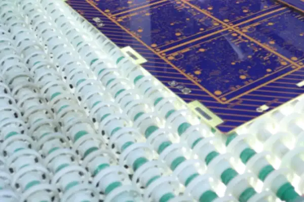
I’ve always found the concept of “stuffing a coin” into a circuit board to be quite fascinating. Of course, I’m not referring to literally inserting a monetary coin; rather, this structural technique—known as a “copper coin PCB”—involves embedding a small block of solid copper into the inner layers during the multi-layer PCB fabrication process.
Many people might assume this is done solely for the purpose of heat dissipation. In reality, that is not entirely the case. I once encountered a specific application in high-frequency circuitry where this method was employed to stabilize impedance fluctuations within the power plane—leveraging the fact that solid copper blocks exhibit more uniform conductivity compared to standard etched copper traces. In that particular instance, the engineers milled a shallow recess into the inner layer; the shape was somewhat unconventional—a hexagon rather than the standard square—a design choice reportedly made to minimize stress concentration. The lamination process is actually quite a rigorous test of manufacturing expertise. You first have to roughen the surface of that small copper coin; otherwise, when the resin flows in, it will slip and fail to bond securely. I once visited a factory and saw that, prior to lamination, they would perform a micro-etching treatment on the copper blocks—it looked just like coating a piece of chocolate with crushed peanuts.
The trickiest part is thickness control. I once received a sample board where I noticed the “coin” area stood two microns higher than the surrounding surface; consequently, it warped during the surface-mount assembly stage. I later learned that this was because the flow characteristics of the prepreg (the semi-cured resin sheet) hadn’t been calculated precisely, resulting in the resin failing to completely fill the void.
In fact, some manufacturers are now experimenting with embedding these copper coins adjacent to the signal layers—not for thermal dissipation, but to serve as electromagnetic shielding. It’s akin to encasing sensitive circuitry within a miniature Faraday cage.
Admittedly, this design does drive up costs—after all, it necessitates several additional manufacturing steps—but sometimes, for the sake of performance, such measures are simply unavoidable.
I’ve always found it fascinating how an antique object like a copper coin can be integrated into the context of modern circuit boards. A while back, while browsing an electronics market, I saw someone using actual antique copper coins as bases onto which they soldered LED chips. While the concept was creative, the practical application was riddled with issues. Antique copper coins suffer from severe surface oxidation and poor conductivity; furthermore, their thickness is inconsistent, making them prone to cold joints during soldering.
It wasn’t until I encountered professional-grade “copper coin PCBs” that I truly understood what industrial-standard thermal management ought to look like. This design—which involves embedding a copper block—is simply in a different league than merely stuffing a loose coin into a board; both its surface flatness and thermal conductivity are the result of precise engineering calculations. I once conducted a side-by-side test, driving a 3-watt LED chip on both a standard aluminum-substrate PCB and a copper-coin PCB. After ten minutes, the aluminum board was too scorching hot to touch, whereas the copper-coin board remained merely lukewarm.
Nowadays, many hobbyists enjoy DIY-ing high-brightness lighting setups but often overlook the critical importance of thermal management. They’ll haphazardly slap components onto any random piece of metal, only to find that light degradation sets in after just a few days. The truly reliable approach involves mounting the heat source directly onto the surface of the copper coin, thereby ensuring that heat is whisked away the instant it is generated. I’ve seen instances where this method was used to construct automotive lighting modules that, even after running continuously for five hours, managed to keep their housing temperatures within a perfectly safe and reasonable range.
Ultimately, what captivates me most about this technology is the elegance it brings to thermal management. It moves away from the clunky, cumbersome combination of bulky heatsinks and cooling fans, opting instead to seamlessly integrate thermal management directly into the very structural fabric of the circuit board itself. The star projector I recently helped a friend modify utilized this very concept: within the confines of a limited housing, a “copper coin” PCB structure was employed to effectively resolve the heat dissipation issues of the LED matrix.
Of course, this manufacturing technique imposes stricter demands on the design process; given the differing coefficients of thermal expansion between the copper block and the FR4 substrate, improper execution can easily lead to cracking. However, when you witness a densely packed array of LED beads operating stably over extended periods, you realize that the upfront investment in design was well worth it. After all, good technology shouldn’t remain confined to the laboratory; only designs that can be successfully implemented to solve real-world problems truly possess vitality.
I have always felt that heat dissipation is the most easily overlooked aspect of circuit board design. It wasn’t until I worked on a car charger project last year that I realized just how scorching hot a tiny Gallium Nitride (GaN) chip could become—too hot, in fact, to even touch. On a traditional PCB, no matter how thick the copper foil layer is, dissipating heat feels like trying to drink boiling-hot porridge through a straw: the heat gets trapped and swirls around beneath the chip, simply unable to escape.
I had a sudden epiphany one day while visiting a factory, where I observed a veteran technician embedding a coin-sized solid copper block directly into a circuit board to cool an LED driver chip. The structure of this “copper coin PCB” is actually quite straightforward: a cutout is created directly beneath the heat source, into which a solid block of high-purity copper is inserted—essentially constructing a dedicated “expressway” for heat to travel along. Compared to relying on thin copper foil for slow thermal conduction, or placing one’s hopes on arrays of vias thinner than a human hair, this simple yet robust approach proves far more effective.
Many engineers today tend to overcomplicate problems; in reality, if you look at the heat sinks found in vintage audio amplifiers, the underlying principles of heat dissipation remain universal. The key lies in providing a sufficiently wide and unobstructed channel for heat to rapidly exit the source area. While the copper foil on a standard PCB offers only two-dimensional heat dissipation, an embedded copper block achieves true three-dimensional thermal conduction. I recall conducting tests using a thermal imaging camera to compare two setups running at an identical 20W power output: the chip surface on the traditional design reached 68°C, whereas the version utilizing the “copper coin” solution consistently remained below 45°C.
Recently, while revising the electronic speed controller (ESC) boards for a drone, I made a point of reserving specific mounting locations for “copper coin” inserts beneath the MOSFETs. Although this increases production costs slightly, when considering the continuous, high-load operation of the motors during flight, I felt the expense was entirely justified. After all, no one wants to see their equipment come crashing out of the sky due to overheating, right? For certain designs, if a solid copper block is the appropriate solution, you shouldn’t skimp on the material costs; attempting to retrofit a heat sink later on will only end up consuming even more valuable space. In fact, this approach should have been widely adopted within the industry long ago. Rather than racking your brains to optimize via density, it is far more effective to simply embed a miniature thermal anchor directly beneath the heat source. The next time you encounter a design challenge involving high heat flux density, consider whether you can equip your critical components with a dedicated metal base; you will find that many thermal management puzzles resolve themselves with surprising ease.
In the field of medical electronics, attention often focuses on complex algorithms;
After years of navigating the hardware industry, I’ve observed an interesting phenomenon:
As a practitioner in the circuit board manufacturing industry, I am keenly
• Expert in Small-to-Medium Batch Production
• High-Precision PCB Fabrication & Automated Assembly
• Reliable Partner for OEM/ODM Electronic Projects
Business Hours: (Mon-Sat) From 9:00 To 18:30