
Heat Dissipation Challenges and Solutions in PCB Circuit Board Design
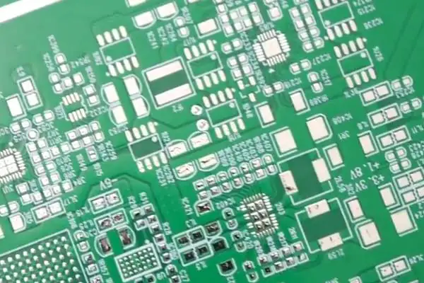
Circuit boards are more than just that green board in a phone
I’ve always felt that many people’s understanding of advanced circuit boards is still limited to the level of “routing tools.” In fact, today’s advanced PCBs are no longer simple connection carriers. Last year, after visiting the laboratory of an advanced PCB manufacturer, I truly understood—those substrates capable of supporting artificial intelligence calculations are more like intricate three-dimensional cities.
One detail was particularly interesting: the cross-section of their sample showed over twenty layers of circuitry arranged like a multi-level transportation system. What surprised me most were the several fingernail-sized copper blocks embedded in the middle for heat conduction. The engineer explained that modern high-end chips operate like small heating elements, which ordinary cooling solutions simply cannot handle. This integration of heat dissipation and circuitry completely changed my understanding of circuit boards.
Previously, I thought choosing a high-end PCB was simply about selecting material parameters. Now I realize the key is understanding how the entire system “breathes.” For example, a friend working on autonomous driving recently had his team struggle with a substrate deformation issue. They later discovered that the difference in the coefficients of thermal expansion of different material layers at high temperatures—a difference of a few micrometers—caused signal distortion. Such problems are impossible to detect by simply looking at design drawings; actual testing is essential.
Now, I increasingly feel that when choosing an advanced PCB supplier, it’s not just about how many layers they can produce; more importantly, it’s about whether they have a database of experience handling abnormal situations. In a previous project, during the final stage, an unexpected high-frequency signal attenuation was discovered. The supplier immediately pulled up a similar case from five years ago and provided a modification plan. This kind of accumulated experience is the truly valuable part.
What impresses me most is the speed of change in this industry. Technologies considered cutting-edge five years ago are now basic. Like when HDI boards first appeared, everyone thought they were groundbreaking; now even smartwatches use similar technology. So, instead of chasing the latest specifications, finding partners who can iterate alongside you is more important. After all, even the most advanced technology ultimately needs to be applied in real-world scenarios.
I’ve always felt that many people’s understanding of PCBs is stuck ten years in the past. They still think it’s just a green board. But today’s advanced PCBs are far more than simple connectors. I’ve seen samples from a high-end PCB manufacturer. They embedded sensors directly into the board. The entire device was as thin as a credit card. This level of integration has completely changed product design thinking.
Previously, when making electronic devices, you had to consider where to put the power module and where to place the antenna. Now, all of these can be integrated into the board itself. I remember a client who made medical devices. They needed to integrate ECG monitoring into a watch, which was achieved using advanced PCB technology. Those intricate analog circuits were directly fabricated on a flexible substrate, ensuring signal quality while saving space.
Some worry that such highly integrated designs will affect ease of repair. However, the reality is that electronic products are updated so rapidly that repair has become a secondary consideration. The more important factor is how to achieve more functionality within a limited space.
I particularly enjoy observing the creativity of different manufacturers in handling heat dissipation issues. Some create microchannels between multilayer boards. Others use special substrates for direct heat conduction. These innovations are often more valuable than simply pursuing smaller linewidths.
A recent case impressed me deeply. A team used advanced PCB technology to integrate the entire RF system into an eyeglass frame. This would have been unimaginable five years ago.
In fact, the key to judging whether a PCB manufacturer truly masters advanced technology is their ability to create customized solutions based on specific application scenarios.
Now even consumer products are starting to pursue this highly integrated design approach.
Sometimes I think, perhaps in the future we won’t need to distinguish between PCBs and chips.
This trend of integration is already very clear.
I see more and more designers treating the PCB as the skeleton of the entire product.
Instead of drawing the circuit diagram first and then considering the layout as in the past,this shift in mindset is actually more important than specific technological breakthroughs.
After all, even the most advanced processes require a suitable design philosophy to realize their value.
Some senior engineers I know are more receptive to this change.
They have experienced the entire development process from through-hole components to surface mount technology.
Therefore, they are highly accepting of the current trend towards integration.
On the other hand, young people just starting out sometimes overly rely on software simulations and ignore the limitations of actual manufacturing processes.
Good design should find a balance between ideal and reality.
It should fully utilize the possibilities offered by advanced PCBs.
It should also clearly understand the boundaries of current manufacturing processes.
This requires designers to have a deep understanding of materials and processes.
It’s not simply about being able to operate design software.
Sometimes the simplest solution is the most effective.
I’ve seen a case where a client initially wanted to use the most complex eight-layer board solution.
Later, they discovered that by optimizing the routing, a four-layer board could meet all the requirements.
This not only reduced costs but also improved the yield rate. Therefore, pursuing advanced technology does not equate to blindly piling on technical specifications.
The key lies in appropriately utilizing suitable processes to achieve design goals.
Recently, I’ve noticed an interesting phenomenon while chatting with some friends in hardware development—many people oversimplify advanced PCB design. They believe that simply handing over the circuit diagram to a high-end PCB manufacturer will solve everything, which is a significant misconception.
I recall a team developing medical devices last year who skipped thermal simulation during the design phase, only to discover chip overheating issues during mass production. Such cases are not uncommon in the industry. Modern high-density circuit boards are like miniature city planning; power routing is like main roads supplying power, and signal lines are like traffic flow in alleyways. Without proper traffic planning during the design phase, the entire system will fall apart.
What I find truly interesting is that current design tools can simulate real-world physical phenomena. For example, you can see current flowing like water in wires and how heat dissipates from heat-generating components. This simulation isn’t just for show; it can detect problems invisible to the naked eye in advance. Once, through electromagnetic simulation, we discovered that a certain antenna design interfered with a sensor, something that might have only been detected during sample testing previously.
When choosing advanced PCB manufacturers, I particularly value their engineering feedback capabilities. Good manufacturers don’t just passively accept orders; they offer suggestions from a manufacturability perspective. For example, once, our designed pad dimensions were too small, and the manufacturer’s suggestion to adjust them directly improved the yield rate by 15%. This kind of experience cannot be learned from textbooks.
Designing flexible circuit boards is even more interesting. Unlike traditional circuit boards, they are not rigid and require consideration of stress distribution during bending. We developed a wearable device where the circuit board needed to withstand tens of thousands of wrist bends without failure. This required simulating various bending scenarios during the simulation phase to identify and reinforce the weakest connection points.
Now, I increasingly feel that PCB design is like architectural design. It’s not just about circuit functionality, but also factors like heat dissipation channels and mechanical strength. Sometimes, to optimize heat dissipation, we intentionally leave heat dissipation channels, much like ventilation shafts in a building.
What impresses me most is the speed of change in this industry. Technologies that seemed cutting-edge five years ago may now be commonplace. Maintaining a learning mindset is more important than mastering a specific technology, as the next generation of advanced PCBs may bring entirely new design ideas.
I’ve always felt that many people’s understanding of electronic products remains superficial. It’s frustrating to see people only focusing on camera pixels and screen refresh rates when new phones are released. What truly determines a device’s performance are the small components hidden inside—like those meticulously designed circuit boards.
I remember disassembling an old game console last year, which left a deep impression. Although the casing was worn beyond recognition, the internal circuit boards remained stable, sparking my interest in the manufacturers of those boards. For example, the Nintendo Game Boy’s status as a classic is largely due to its robust and durable motherboard design, which continues to function stably even after years of use.
Many electronic products today strive for thinness and lightness, which places higher demands on the arrangement of internal components. Ordinary circuit boards can hardly meet these requirements, necessitating more sophisticated solutions. For instance, in smartphones, engineers need to precisely arrange hundreds of components in an area the size of a fingernail using high-density interconnect technology, requiring advanced processes such as micro-hole drilling and laser imaging.
An engineer I know once showed me a sample design from his team. They integrated the processor and memory directly onto the substrate. This not only reduced the overall size but also improved signal transmission efficiency. This design completely overturned the traditional motherboard layout. This system-in-package (SoC) technology can reduce circuit length by 30%, significantly reducing signal latency and power consumption.
Sometimes I wonder why devices with the same functionality have such different prices. Besides brand premium, the internal materials and processes are key. Products that tout high performance often put more effort into unseen aspects. For example, high-end devices use thicker copper foil layers and better solder mask materials. These details, though invisible to consumers, directly affect the product’s durability and stability.
Recently, while researching smart home devices, I discovered an interesting phenomenon: some manufacturers specifically emphasize that they use circuit boards from certain suppliers. This made me realize that consumers are starting to pay attention to these previously overlooked details. For example, some smart speaker brands specify that they use circuit boards from companies like Nichika or Shengyi Technology, suppliers known for their strict quality control.
In fact, circuit board design is like city planning; it must ensure the functionality of each area while considering future expansion possibilities. A good design can extend a product’s lifespan by several years. For example, reserving sufficient test points and interface locations facilitates later maintenance and functional upgrades; this forward-thinking design often significantly enhances the product’s usability.
Once, I visited an electronics exhibition and saw a manufacturer showcasing a sample board where the power management and signal processing modules were stacked three-dimensionally. This 3D construction method is indeed more innovative than a planar layout. Through this design, they successfully reduced the circuit board area by 40% while maintaining excellent heat dissipation.
Now, more and more devices need to handle complex tasks, posing new challenges to the circuit board’s load-bearing capacity. Traditional double-sided boards are no longer sufficient, and multi-layer boards are gradually becoming the mainstream choice. For example, modern graphics cards typically use 12 or even more layers of circuit boards to accommodate complex wiring and high-frequency signal transmission requirements.
I always feel that evaluating an electronic product shouldn’t just look at the impressive numbers on the specifications sheet; it’s more important to understand its internal structure, just as judging a person’s strength shouldn’t be based solely on appearance but on their inner qualities. For instance, some mobile phones may have high-resolution cameras, but if the circuitry around the image processing chip is poorly designed, the actual image quality can be significantly reduced.
While helping a friend choose a laptop recently, I paid special attention to the internal structure diagrams of various products. I discovered significant differences in materials and layout even among machines in the same price range, directly impacting heat dissipation and operational stability. For example, some brands place more decoupling capacitors around key chips; this attention to detail effectively suppresses power supply noise.
Perhaps in the future, when choosing electronic products, we’ll be like car enthusiasts today, not only focusing on appearance and specifications but also carefully examining the “engine compartment” layout, as this is crucial in determining product quality. Just as car enthusiasts pay attention to engine layout and chassis structure, the core value of electronic products lies in these ingenious internal designs.
I always find those thin circuit boards fascinating. I used to think they were just green boards with a few wires. Now it’s different.
I know a few friends who work in advanced PCB design who often talk to me about the challenges they encounter. One project required making sensors extremely small while ensuring stability. They tried several solutions without success. Later, a senior PCB manufacturer suggested they change their approach and redesign the layout from the packaging stage.
Many innovations actually begin in seemingly ordinary areas. For example, many medical devices now utilize this miniaturization approach. I once disassembled a blood glucose meter and found that the PCB inside was smaller than a fingernail, yet it didn’t lack any functionality.
Flexible circuit boards are also a fascinating area. I’ve seen an experimental product where the circuitry is printed directly onto a stretchable material, allowing it to be applied to the skin like a band-aid to monitor data. This advanced PCB technology makes devices more human-friendly and easier to use.
However, these advancements require the cooperation of the entire industry chain. Material suppliers need to develop new substrates, manufacturers need to update their production lines, and design teams even need to relearn how to use simulation software.
A project I’ve recently been researching encountered a similar problem. We wanted to find a suitable advanced PCB solution, but found that existing standards weren’t very applicable, potentially requiring customized development. This depends on the manufacturer’s technological reserves.
Sometimes, innovation doesn’t necessarily mean pursuing the latest and most dazzling technology. Utilizing existing technology effectively can also produce unexpected results. The key is to find a solution that truly suits your product, rather than blindly following trends and chasing so-called cutting-edge technology. After all, even the best technology needs to be practically implemented, right?
While researching high-end electronic products recently, I discovered an interesting phenomenon—many people focus on the chips but overlook the importance of the circuit board. In fact, a good PCB is like a city’s underground pipe network, determining the overall efficiency of the equipment.
I remember once disassembling a medical device and seeing the intricate wiring layout, so precise it was like a work of art. Those hair-thin traces made me realize that the complexity of modern electronic products far exceeds our imagination. Choosing a reliable, high-end PCB manufacturer can indeed bring a completely different product experience; their control over trace width directly affects signal transmission quality.
Many manufacturers are now pursuing smaller package sizes, which places higher demands on PCBs. Traditional PCB design approaches are no longer sufficient; we need advanced PCB solutions capable of supporting complex functions, especially in high-frequency, high-speed applications where the dielectric constant and loss factor of materials become particularly critical.
I’ve seen some failures where the use of unsuitable substrate materials led to signal integrity issues across entire batches of products. This has taught me that electromagnetic compatibility (EMC) must be considered during the design phase, not just addressed after mass production. Excellent engineers will simulate various operating conditions in advance to ensure every step is flawless.
As devices become increasingly feature-rich, the number of circuit board layers is constantly increasing, from simple double-sided boards to multi-layer boards with dozens of layers. This evolution reflects continuous advancements in manufacturing processes. In particular, the emergence of arbitrary-layer interconnect technology has allowed for unprecedented wiring density, making product miniaturization possible.
Sometimes I wonder why devices with the same functionality have such vastly different prices. Only after seeing different levels of PCBs firsthand did I understand that the greatest value often lies in the unseen details. A meticulously designed advanced PCB can indeed improve overall performance; this is probably what is meant by “details determine success or failure.”
With the rapid pace of electronic product updates, the requirements for PCBs are constantly changing. The future may see more flexible and foldable circuit boards, which presents new challenges to materials and processes, but is also an inevitable trend in industry development.
I’ve always felt that many people have misconceptions about high-end circuit boards. They always think that simply making the lines finer will solve the problem. In reality, the true determinants of an advanced PCB’s success often lie in the unseen details.
I remember visiting a high-end PCB manufacturer’s lab last year. They were testing the heat dissipation performance of different substrates. An engineer showed me with a thermal imager that the temperature difference of the same chip on different materials could be over twenty degrees Celsius. This made me realize that material selection is far more important than we imagine. For example, in the aerospace field, circuit boards need to withstand extreme temperature changes and vibration environments. In such cases, ordinary substrates like FR-4 are far from sufficient; special materials such as polyimide or ceramic substrates must be used. Although these materials are more expensive, they ensure that the equipment maintains stable operation under harsh conditions.
Currently, some manufacturers on the market prioritize impressive specifications by making the circuitry too dense, neglecting the most basic heat dissipation requirements. I’ve seen too many cases where entire batches of products had to be reworked due to substandard materials. This is especially true for equipment that requires long-term high-load operation; if the base material is chosen incorrectly, subsequent optimization is futile. Take automotive electronics as an example: the engine control unit needs to operate continuously in a high-temperature environment. If the thermal expansion coefficient of the substrate doesn’t match the components, mechanical stress will occur, leading to solder joint cracking. Such failures often only manifest after a period of use, posing safety hazards to end users.
Recently, a friend working in industrial control complained to me that the PCBs they purchased frequently experienced inexplicable failures, which were later discovered to be caused by micro-deformation of the substrate material under high temperatures, leading to poor contact. This type of problem is difficult to detect in routine testing but directly impacts equipment reliability. In fact, professional manufacturers conduct thermal simulation analysis during the design phase, predicting potential problems by simulating the actual operating temperature field. They may also use materials with higher glass transition temperatures, such as Isola’s 370HR series, which maintains stable mechanical properties even at 150°C.
In fact, judging the quality of an advanced PCB cannot be based solely on technical parameters; the actual application scenario must also be considered. For example, the requirements for circuit boards used in medical equipment and communication base stations are completely different; the former prioritizes stability, while the latter must also consider high-frequency performance. A good manufacturer should be able to recommend the most suitable solution based on customer needs, rather than simply pushing the highest configuration. In medical imaging equipment, circuit boards may need to pass biocompatibility certification, while 5G base station circuits require special attention to the stability of the dielectric constant as a function of frequency. These specialized requirements often necessitate manufacturers possessing interdisciplinary knowledge. Sometimes the simplest solution is the most effective. Instead of blindly pursuing the latest technology, it’s better to thoroughly understand the fundamental materials. After all, even the most complex designs ultimately come down to specific substrates and circuits. If these fundamental components fail, even the most advanced technology is just a castle in the air. For example, in high-speed digital circuit design, many people only focus on signal integrity simulation, neglecting the dielectric loss of the substrate material. When signal rates reach 25Gbps or higher, the loss factor of ordinary FR-4 material becomes a bottleneck, necessitating the use of low-loss specialty materials such as Megtron-6 or Tachyon-100G.
I firmly believe that experience is more important than theory in this industry. I’ve seen too many designers who only talk the talk but don’t walk the walk; their drawings may look beautiful, but they can’t withstand the test of actual production. Truly excellent engineers often understand how to balance the gap between ideal and reality. They know when to adhere to design specifications and when to compromise based on manufacturing processes. For example, in impedance control, experienced engineers will communicate with manufacturers in advance to adjust the trace width according to the actual board parameters, rather than rigidly adhering to theoretical calculations. This practical wisdom often avoids significant losses during mass production.
Circuit boards are more than just that green board in a phone
From disassembling old routers to visiting electronics manufacturing plants, I gradually realized
As an electronics enthusiast, I’ve come to understand firsthand the impact of
• Expert in Small-to-Medium Batch Production
• High-Precision PCB Fabrication & Automated Assembly
• Reliable Partner for OEM/ODM Electronic Projects
Business Hours: (Mon-Sat) From 9:00 To 18:30