

Programmable Automation Controller PCB: How Copper Weight, Lamination Quality, Bus Topology, and Thermal Design Decide PAC Backplane Reliability
A PAC rack is only as reliable as its backplane. Inner-layer copper
For wireless EV charging, the PCB is not a passive wiring board; it is the crossing point of high-frequency power, small signals, magnetic fields and heat. Moving from 85kHz to 6.78MHz makes skin and proximity effects, parasitic inductance in the commutation and gate loops, dielectric loss, copper thickness tolerance and etch compensation decide whether a prototype runs or burns. This article collects hands-on lessons on a Wireless EV Charging PCB: why heavy copper is only the first step, how GaN gate loops and hidden diode footprints are handled, how foreign object detection (FOD) is corrupted by switching harmonics, and how thermal shock, Z-axis expansion and lamination quality cause delamination. It also explains how to question a heavy copper PCB supplier or a multilayer PCB manufacturer, using cross-section reports, measured resonance data and mass-production experience instead of quoted copper weight or price. A short FAQ follows at the end.
In the past two years I have handled several wireless EV charging projects, from the earliest 85kHz all the way to the later ones where someone insisted on 6.78MHz, and the pits I stepped in could fill a laboratory. I find that the industry is now a bit over-enthusiastic about the MHz band, especially some start-up teams, who talk about magnetic resonance and spatial freedom at every turn, as if all problems would be solved once the frequency goes up. Anyone who has really built a Wireless EV Charging PCB knows in their heart that on the 6.78MHz road the board-level cost of implementation is much larger than imagined.
Take finding suppliers as an example. In the 85kHz days, the market was full of factories that could make a power board well, and finding a reliable Heavy copper PCB supplier was not hard: four-layer and six-layer boards with thick copper, carrying a main loop of around one hundred amps, had stable yields. But once you switch to the MHz band, at the same power level the copper thickness cannot come down, while skin effect and proximity effect squeeze the current into the few microns at the surface of the copper foil, and the heat generation climbs in somersaults. If you then contact those conventional multilayer pcb manufacturers, they hesitate even when sending the quotation once they hear you want to run tens of amperes at 6.78MHz while controlling interlayer capacitance and magnetic coupling. Later our team stubbornly tried four different Heavy copper PCB manufacturers: either the dielectric loss tangent was too large, or the lamination structure could not take thermal shock, and the boards that came back from prototyping blew the GaN gates in less than half an hour after being installed.
Many people think that going to MHz lets the magnetic coupler be made as thin as a cookie and makes vehicle packaging much easier, but the difficulty of physically reconstructing the board itself eats up that little space advantage directly. I remember one time vividly: we tried to integrate the resonant inductor and the coil into a “magnetically integrated module”. At 85kHz a standard LCC topology was used, and in the PCB layout it was enough to reduce the commutation loop area, with the parasitic parameters basically still within the prediction of the lumped model. But at 6.78MHz, even the mutual inductance between two parallel copper traces can distort the gate drive waveform beyond recognition, not to mention the leakage inductance of the planar transformer that you thought had no effect. A young engineer spent a long time measuring with a network analyzer and found that the frequency characteristics of the whole power loop deviated completely from the simulation result. The problem lay in the stackup data provided by the multilayer pcb supplier, which had omitted the actual dielectric constant of one prepreg layer. At low frequency this would at most cost a point or two of efficiency, but at MHz it directly triggered chained oscillations, and the drive power consumption was far higher than the theoretical value.
The gate drive account cannot be left out either. Both are wide-bandgap devices, but SiC and GaN perform very differently in this band. We measured a 1200V SiC module whose gate drive circuit alone, at full power at 6.78MHz, consumed auxiliary power almost equal to the power adapter of a small laptop, and that small driver area glowed in the thermal imager in a way that made you uneasy. After switching to GaN the auxiliary power came down, but the gate’s tolerance of layout stray inductance came down too, forcing you to squeeze the drive loop to the limit, and the board material and process all had to be re-evaluated, so in the end you are back in the endless loop of negotiating with a Heavy copper PCB supplier: you want thick copper, ultra-low dielectric loss and mixed multilayer lamination all together, and the factories that can do all of these can be counted on two hands.
In my view, pushing in-vehicle wireless charging fully to MHz at this stage looks more like a collective failure of physical assumptions. Nobody dares to trust results computed by looking up tables in the lumped parameter system, and EMI cannot be fudged by adding a common-mode choke and a few Y capacitors as in the low-frequency band. Every trace on the board turns into an antenna, coil near-field leakage and PCB edge radiation crosstalk mix together, and when you do a pre-compliance test, the spectral components on the analyzer are dense as a fence. So when I talk about this topic with people now, I always first urge them to think clearly: unless you must pursue extremely small volume or dynamic alignment capability, there is nothing shameful in honestly staying at 85kHz. If you really go to MHz, then treat the PCB itself as a microwave device, and from the very beginning drag the most knowledgeable Heavy copper PCB manufacturer and multilayer pcb supplier into the project together, throwing out and redoing everything from material selection to stackup design, and only then do you have the capital to continue. Otherwise, however beautifully the drawing is made, what comes back from the fab is a pile of burnt-black copper foil.
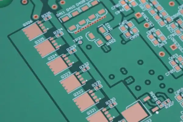
When I worked on wireless charging projects for electric vehicles in the past, I did not at first feel that a PCB could cause any trouble. Just carry the current and connect a few components; find a multilayer board supplier, stack it up with the conventional scheme, and as long as the inductance value is calculated right, it is done. As a result, when the board came back and was powered up, pushing the frequency to 6.78 MHz gave me a lesson directly: the driver area was so hot I could not hold my hand on it, and efficiency dropped outrageously. Only then did I realize that in the MHz band the PCB is no longer what it used to be.
On review, the pits were basically all stepped in the same place: parasitic inductance. Think about it: the commutation loop is only a small ring of trace, and a few extra nanohenries can drag the loss up a great deal through the spike at the switching instant, and all that heat is trapped in the small area of the gate drive and cannot get out. At that time I tried three or four heavy copper pcb suppliers in a row. Some claimed they could make thick copper, but above 10oz they could not control etching precision, the line width consistency was unwatchable, and at high frequency the skin effect directly made the equivalent impedance drift. Only when I met a heavy copper pcb manufacturer that specialized in heavy copper, who knew how to balance high copper thickness against interlayer bonding strength, did thermal management finally have a foundation.
There are also many twists and turns in multilayer boards. It is not the case that any multilayer pcb manufacturer can stack a few layers and have it work; how to arrange the traces and how to interleave the layers so that part of the magnetic flux cancels out is a very deep subject. I tried an ordinary four-layer board and the radiation exceeded the limit directly; later I changed to six layers and flattened the current loop, and only then barely passed. Many people tend to think too narrowly about inductance, staring only at the few turns of the coil, but at MHz the inductance of vias, pins and even the return path of copper pour all jump out to make trouble. The magnitudes are not large but their sum is enough to give you a hard time. So later I directly required the multilayer pcb supplier to run simulation that models proximity effect and skin effect together, instead of looking only at the nominal inductance value and calling it done.
Put this way, moving a wireless charging PCB toward MHz is not a simple matter of swapping the components for high-frequency ones. From copper thickness to stackup, from trace inductance to the underlying magnetic materials, the whole physical model has to be rebuilt in your head. The old “good enough” way of thinking does not even need to be tried in this band.
In these years of wireless charging work, I have increasingly felt that a good PCB is not finished when the circuit is drawn. Many people put all their energy into the topology and magnetic coupling design and just find any multilayer board factory to prototype the board, feeling that as long as it connects, it is fine. As a result, once power is applied, especially when running near megahertz, the whole board turns into a scalding heat source and efficiency drops in a mess. I did the same at the start, and only after paying for it did I understand that a Wireless EV Charging PCB is a completely different thing from an ordinary digital board: with high current density and high frequency, many physical laws will hard-pull you back to reality.
At that time we were building an 11kW demonstration prototype, and the transmitter side used a standard four-layer board with 1oz copper. Everything was normal during the earlier debugging, but when the frequency was raised from 85kHz to several MHz for testing, the power consumption of the auxiliary supply section suddenly ran out of control, and the copper ring around the drive resistor blistered directly. When taken apart, it was not a device selection problem; the PCB itself could not stand the heat accumulation on the current path. Put plainly, the copper was not thick enough. The copper foil of an ordinary board offers too much resistance to pulsed current of tens of amps, all the power loss turns into heat, and it piles up in an area of a few tens of square millimeters and cannot spread. The temperature did not rise slowly; within a few seconds it could blister your hand.
After that I started looking everywhere for a Heavy copper PCB manufacturer, and the process was not easy either. There are many factories that can do thick copper, but very few that can do thick copper while also controlling line width accuracy and withstand voltage. What we needed was not simply to thicken the copper but to let thick copper carry the large-current bus in the multilayer structure while other layers still carried small signals and logic control, which needs a multilayer pcb manufacturer with a very mature lamination process; otherwise the layers delaminate easily, or uneven copper thickness causes local impedance jumps. The biggest advantage of a thick copper board is not only lowering DC resistance; its ability to absorb and carry transient heat is far stronger than thin copper, equivalent to installing an invisible heat-dissipation skeleton in the PCB. The power consumption is still there, but hot spots do not accumulate easily, and only then did thermal design at high frequency have room to operate.
Once the frequency reaches the MHz level, multilayer board design is no longer only mechanical stacking. You find that the integrity of the ground plane and the length of the return path directly decide whether the board works stably. In one of our designs, just changing the position of a via reduced the loop inductance a lot, and the ringing on the switching waveform clearly converged. Only then did I realize that parameters such as the interlayer dielectric thickness and glass cloth type provided by the multilayer pcb supplier are not decorations; they genuinely affect impedance continuity and signal return. Many times a sharp rise in power consumption is not because device losses increased but because parasitic parameters on the PCB rang away the energy during switching, and all that loss is concentrated on the board, so the power consumption you measure is naturally outrageous.
I think the supplier selection step cannot be overstated. A reliable heavy copper pcb supplier dares to tell you what uniformity they can achieve in copper thickness, instead of thumping their chest and saying the maximum can reach 20oz when the actual deviation is huge, with thin corners and a thick middle. Likewise, if a multilayer pcb supplier proactively discusses with you the influence of solder mask ink on high-frequency dielectric loss rather than just hurrying you to place an order, that factory is basically dependable. Sometimes a price difference of twenty or thirty percent hides a huge gulf in yield and long-term reliability. The one we later cooperated with regularly has quite strict acceptance standards for the plating capability of thick copper boards, and every batch of boards comes with a copper thickness distribution map under thermal imaging; a supplier like this saves you a lot of worry.
Looking back now, the essence of a Wireless EV Charging PCB is a physical channel for energy: it must not only connect the devices but also bear and channel large current and high-frequency fields. If heavy copper and multilayer design are done well, power consumption and heating are much lower and a large cooling cost can be saved. Many people ask me why I do not use a more complicated cooling scheme, and I say do not rush to add fans and water cooling; make the PCB copper a bit thicker and the stackup a bit more reasonable, and many thermal problems disappear on their own. The board itself is the first cooling system, and if you ignore this, no matter how much you spend on peripheral cooling, you cannot repay the debt owed to basic physics.
Some time ago I helped a customer evaluate a receiver-side board for in-vehicle wireless charging, with a power of about 11kW and a frequency set at 6.78MHz. The customer asked right away whether an ordinary multilayer board could be used directly, and as soon as I heard it I knew this was not so simple. Under high-frequency heavy current, if the copper is not thick enough the temperature rise of the traces cannot be held down, especially near the gate loops of the GaN devices, where if the current path is a bit longer the parasitic inductance rises and ringing makes the switching waveform shake until it cannot be looked at. I had been burned before: I had stubbornly used a multilayer board with standard 2oz copper to run a MHz-class half bridge, and the gate voltage showed a very obvious dip on the rising edge; later investigation showed that the drive loop and the device input capacitance were resonating near 9MHz and just happened to be excited.
Later I learned my lesson: for any design of this type, I first talk with the heavy copper pcb supplier and ask clearly how thick they can really pile the copper, and it must be a factory that can still guarantee line width accuracy after plating. Some factories claim to make thick copper, but actually only the outer layers are laminated with thick copper foil while the via barrel copper is still a thin layer, and once heavy current hits, the via becomes the weak point. I habitually look for a heavy copper pcb manufacturer who can make copper thickness of 4oz or more and whose via wall copper thickness can keep up with the outer foil thickness, so that the thermal capacity and impedance of the whole current path stay consistent.
Another experience also left a deep impression. That board used GaN, and I deliberately shortened the gate drive loop to within 5 millimeters, but at the beginning of layout, because it was a multilayer structure, the gate signal changed layers back and forth, two extra vias were added, and the simulated inductance of the whole loop came to nearly 3nH. Do not look down on this small number: at the switching edges of 6.78MHz the gate spike could rush above 6V, and a normal 5V driver chip simply could not stand it. In the end, with no way out, I put the whole gate drive loop on the top layer, hollowed out the inner layer to use as a shielded reference, placed the driver chip tight against the GaN gate pin, and then enlarged the local copper area for natural-convection cooling, and only then was the junction temperature brought to an acceptable range. This also made me realize that many multilayer pcb manufacturers do not understand the special needs of high-frequency power; they just do conventional impedance control, and you have to watch the layout and stackup strategy yourself.
Speaking of cooling, many people now blindly believe in the “low auxiliary power” of GaN, feeling that if it generates little heat you need not consider it further. In fact, once the reverse conduction loss at MHz is added to the extra switching loss caused by high-frequency oscillation, the total heat is not small. I do not much believe in the claims that “no freewheeling diode is needed”; every time I leave a place for a Schottky diode on the PCB, and even if I do not solder it during early debugging, I must build the pad and the thermal vias in. This “hidden space” is something many people designing a wireless charging transmitter for the first time overlook, and if you add it after finding that the waveform is wrong, the board revision cycle is lengthened for nothing.
So my habit is that when looking for a multilayer pcb supplier to make this kind of board, I state requirements directly: the interlayer dielectric thickness must support a low-inductance loop, certain layers must be designated thick copper, and I confirm that their solder mask opening and copper spreading capability can meet the cooling need of my local hot zone. Business has to be this direct; do not expect that throwing over one Gerber file will run smoothly by itself, especially for something like the Wireless EV Charging PCB where power, high frequency and heat are interwoven. You have to find out the supplier’s process boundaries in advance, otherwise when the board comes back and is powered up you will be dumbfounded.
I have been in contact with the electric vehicle wireless charging business for almost three years, and my biggest feeling is: never be fooled by the pretty percentages in papers. If you read a review, it will tell you that an interleaved layout can make loop inductance drop by 63% in an instant, and the calculated result makes it seem as if changing to a different stackup structure would solve the deadly switching noise at MHz. But when you actually draw the board and look for a manufacturer, you find that not one of the earlier pits has gone away.
Inductance, on the drawing, is just a simulation result, but once it reaches the factory, if the heavy copper PCB supplier slightly changes the etch factor of the copper foil, or the dielectric thickness drifts a little during multilayer lamination, the magnetic field cancellation effect you spent two weeks optimizing is directly discounted. What is more annoying is that many multilayer PCB manufacturers are simply unwilling to cooperate on tightly coupled layer pairs with extremely thin dielectric, because they do the yield arithmetic. You have to state your requirements clearly, and even go to the production line yourself to watch the first article, before you can get a board whose impedance and coupling are barely acceptable.
One more point left a particularly deep impression: stress amplification from resonant voltage. Many people in the industry, whenever MHz wireless charging is mentioned, stare only at switching loss and EMI, but what really breaks people during system debugging is the voltage spikes on the resonant tank. If the Q of the resonant network you design is high, under light load or slight detuning the voltage across the capacitor can directly threaten the device voltage rating. At this point it is not the case that finding a multilayer pcb supplier to make the board in thick copper settles everything. Thick copper only solves the over-current temperature rise problem; if the layout of the inductor traces makes the loop area large, the voltage ringing brought by the peak of the resonant current makes the whole board radiate outward like a small radio station.
On the Wireless EV Charging PCB, I now tend to see stackup design as an art of compromise rather than the optimal solution in a paper. The so-called enhanced current distribution and magnetic field cancellation are in essence trading space for performance. If you want to free up adjacent layers on the board for power commutation and gate return, it means some signals have to take the long way around or add vias to change layers. And the parasitic inductance of a via in the MHz band is not a negligible small quantity at all; sometimes, in pursuit of a tightly coupled commutation loop, the two or three extra vias punched in pull the effort right back to the origin.
So I gradually lost the patience to argue with people about which layout can reduce inductance by what percentage. What I value more is whether the multilayer board manufacturer can stably control the dielectric thickness for me, whether they can combine thick copper with fine lines, and whether the waveform I measure myself on the bench after the board comes back is clean. Because in the end, the ideal conditions in the simulation fall onto real materials, and the only thing that can verify them is the board you have just taken out of the reflow oven.
Over the past few years I have been following all kinds of wireless charging projects, from the initial few watts of phone charging to the tens or even hundreds of kilowatts of electric vehicle wireless charging now, and my biggest feeling is that the PCB has been seriously underestimated. Everyone talks about topology, coil design and magnetic coupling, but few treat the PCB itself as a key component. I think this is a huge blind spot, especially when you push the frequency to the MHz level.
In earlier years we used industrial-grade multilayer boards for a 6.78MHz system and went to a conventional multilayer pcb manufacturer, whose stackup recommendation followed the signal integrity way of thinking, with copper thickness basically at 1oz or 2oz at most, because they assumed high-frequency traces only need to consider skin depth. But what runs on a Wireless EV Charging PCB is high-power resonant current, whose peak is several times the average; skin effect is only one of the troubles, and the bigger problem is that the copper cross-section is simply not enough. Later we were forced to find a Heavy copper PCB supplier ourselves, trying from 4oz to 6oz, and in some extreme projects even evaluating 10oz copper thickness, and only then found that the fundamental problem was not insufficient copper thickness but that, at such non-standard copper thicknesses, the etching accuracy and layer-to-layer alignment of the multilayer pcb supplier fell off a cliff. Once the line width loses control, the frequency of the resonance point drifts, and at MHz a deviation of a few hundred kHz makes efficiency drop to an unwatchable level.
There is an experience here that is rarely mentioned: traces cannot be sized by current-carrying capacity alone. At MHz the trace itself is part of the resonant network, and its parasitic inductance directly participates in the resonance; tiny deviations in copper thickness and line width change this inductance value. We paid for this: we found a factory that claimed to make heavy copper PCB, and when the prototypes came back and were measured, the resonant frequency differed from the simulation by nearly one megahertz. After two months of investigation we finally found that when doing trace compensation they had applied a large etching factor based on DC experience, so the actual line width was narrower and the inductance went up. Nobody cared about such deviation in the kHz era, but at MHz it is fatal.
So when I look at PCB suppliers now, I no longer care how many oz of copper they claim they can make; I care more about their understanding of the process for high-frequency heavy current. A qualified Heavy copper PCB manufacturer should be able to discuss with you the simulation of current density distribution at different frequencies, instead of tossing you a chart from IPC-2152. If the internal copper thickness of a multilayer board at MHz is allocated unreasonably, the inner-layer copper foil becomes a hot spot because of poor heat dissipation, and that position happens to be the trace node from the resonant capacitor to the coil, where a high temperature collapses the life. These are things you only understand after really blowing up a machine, and textbooks do not write them.
I have been involved in quite a few in-vehicle wireless charging projects, and after going round and round I found something rather helpless: everyone spends too much energy on magnetic circuit simulation and coil optimization, but what actually drags things down is often that unremarkable PCB. However exquisitely the coil is designed, once it is installed in the vehicle and runs, heat and vibration can throw off every precise calculation. Especially as output power goes up, you find that the copper thickness of an ordinary PCB simply cannot bear the temperature rise brought by large current, not to mention that after long-term thermal expansion and contraction, tiny delamination between the copper foil and the base material quietly changes the electrical parameters of the coil. This is why I am now more willing to deal with suppliers who have done heavy copper PCB: not because they can print thick copper, but because they understand how the change in thermal path brought by thick copper reacts back on the stability of the coupling coefficient.
Many people treat misalignment purely as a problem of mechanical installation tolerance, and I think that is a bit narrow. Seen from the PCB manufacturing step, misalignment actually starts when the copper-clad laminate is cut. If expansion and contraction control in the multilayer lamination process is not stable, the relative position of each layer of coil shifts, and this kind of microscopic misalignment simply cannot be made up by external mechanical adjustment. You get a multilayer PCB whose coil pattern looks right, but when it works in a high-frequency magnetic field, the capacitive coupling between inner layers produces extra loops from that tiny misalignment. I have seen a team spend three months tuning the resonant network, only to find in the end that the supplier’s layer-to-layer registration accuracy was insufficient, making the mutual inductance of the two coils differ from the design value by nearly seven percent. For a manufacturer that has never run vehicle-grade heavy copper PCB in volume, this is almost an unsolvable pit.
From another angle, coupling is not only the magnetic coupling between coil and coil; electric field coupling inside the PCB is equally thorny. The side of a thick copper trace has no extra solder mask protection, and when current density concentrates at the edge of the line, the electric field stress between adjacent conductors makes the parasitic capacitance deviate from the theoretical estimate. The more you try to raise the coil’s quality factor by shrinking the line spacing, the more obvious this parasitic effect becomes. I have seen the impedance control reports given by several multilayer PCB manufacturers, and the deviation between measured and simulated values at 6oz copper thickness is far larger than on a conventional 1oz board; in other words, which heavy copper PCB supplier you choose determines, to some degree, whether your coupling design is running simulation or just talking on paper.
So when I take part in such projects now, my thinking is reversed: first find a multilayer pcb supplier that can run a stable thick copper process, get their actual machining tolerances, dielectric thickness and copper foil profile data, and only then do the coil simulation and matching. The shape and number of turns of the coil are actually not the first things to be fixed, because process capability decides the ceiling of the design. Some manufacturers can make 10oz copper thickness and guarantee line width accuracy within ±20%, and this capability directly widens your current-carrying boundary, so that you can even consider greater misalignment tolerance and cover worse parking scenarios. Otherwise, however perfectly you align in the lab, once the position moves the impedance of the whole system drifts, and that is not an inherent problem of the coupling coil; it is that the foundation was not laid firmly.
Not long ago a customer building a wireless charging post talked with me about a ground-side transmitter PCB that behaved fairly stably at the prototype stage, but problems appeared in clusters once it reached small-batch production. The most troublesome were heating and inexplicable signal drift, especially when the load changed and the resonance point of the whole system wandered. They sent me the schematic and layout to look at, and at one glance I noticed that the board used conventional 1 ounce copper and was made by an ordinary multilayer board manufacturer specializing in quick-turn prototyping.
This choice, in a scenario transmitting hundreds of watts, was simply digging a pit for themselves. The transmitter coil of wireless charging works at tens to hundreds of kHz, but once GaN or SiC switches are involved, the harmonic content of the current waveform can easily climb to the MHz level. Many people think this is just a simple low-frequency high-current circuit that can be handled by a standard PCB process, but in fact the skin effect and proximity effect brought by high-frequency harmonics make the effective conducting area of the copper foil shrink sharply and the loss multiply. At these frequencies the temperature rise curve of conventional-thickness traces is not linear at all, and local hot spots may be twenty or thirty degrees higher than the simulation result.
I advised them to switch at once to a supplier dedicated to heavy copper PCB, not the kind that can only make single or double-sided thick copper but one that can handle mixed lamination of multilayer thick copper. Because the power loop of wireless charging needs 4 ounce or even 6 ounce copper on inner layers to carry large current, while the signal control part needs fine dense traces, and this mixed structure demands outrageously high lamination process and layer alignment. When an ordinary multilayer board manufacturer meets such a requirement, it either refuses the order outright or barely makes it with terrible inner-layer copper uniformity, leading to loss of impedance control. Later they found a supplier with real mass-production experience in heavy copper multilayer boards, and after re-prototyping, the heating problem dropped by two orders of magnitude.
Thickening the copper on the PCB is only the first step. Another easily overlooked point is that the ground plane strategy of the whole board is a completely different game in the MHz band. In the kHz band we are used to relying on large-area ground pour to handle EMC, hoping a low-impedance return will swallow all the noise. But at tens of MHz, that ground pour itself starts to become a resonant cavity. The most typical case I have seen was the auxiliary power module on the receiver side, whose switching frequency happened to fall on a certain MHz point and, through the distributed capacitance between the internal ground layer of the PCB and the power coil, formed a perfect common-mode radiation path, directly interfering with the CAN bus next to it until it reported errors constantly.
The way to solve this is no longer something simply thickening the copper can do. In the layout stage you must deliberately dismantle the current loops and split the ground layer under the high-speed switching nodes, forcing the noise current to follow the path we designed instead of running everywhere. This tests the process capability of the multilayer board manufacturer very much, for example the flatness of copper filling in buried and blind vias and the tolerance control of dielectric thickness. Once I took an eight-layer design to suppliers, with third-order blind and buried vias inside and also an attempt at locally mixed FR4 and high-frequency board material; almost all prototype shops shook their heads and said the yield was too low. But a multilayer board manufacturer with real R&D capability will sit down with you to discuss stackup optimization instead of throwing out a flat “cannot do”. They will tell you between which two layers to add a high-resin-content prepreg, which can significantly improve the contradiction between high-voltage isolation and distributed capacitance.
On inductors, I think there is a very interesting trend now. To relieve the PCB, many people want to move the resonant inductor off the board and integrate it directly into the magnetic coupler, for example in topologies such as LCC-S. The direction itself is fine, but the consequence is that the PCB design pressure at the front end is not reduced; it is converted into a more complicated electromagnetic compatibility challenge. Because once most of the physical volume of the inductor leaves the PCB, the switches, rectifier bridge and sampling circuits remaining on the board are exposed to a stronger near-field magnetic field. Especially in detuned conditions, the magnetic field around the coil redistributes and may couple a mV-level offset into the ADC sampling pin, which varies with the load phase and cannot be filtered out. I scanned with a near-field probe on the test bench: for the same board, between the coil aligned and deliberately offset by 5 centimeters, the MHz envelope measured under the crystal differed by as much as 15dB. A conventional conducted emission test cannot measure this at all, because the excitation conditions are so special.
So the real chokepoint in wireless charging PCB design, especially automotive grade, is not how ingenious the schematic is but whether you can find the supplier who is willing to grind through the process details with you.
Now many people talking about wireless charging stuff the inductor into the magnetic coupler at every turn, as if moving work off the PCB were technical progress. I think this approach is a bit like abandoning the root for the branch. What is really hard about a Wireless EV Charging PCB is not that there is no place to put those few inductors, but whether the copper foil can hold up and the heat can be dissipated while tens of amperes run continuously. Instead of racking your brains winding wire on a magnetic core and worrying that air gaps and assembly tolerance affect the coupling coefficient, it is better to honestly find a reliable Heavy copper PCB supplier. With a thick copper board, ceramic base or directly 4oz or 6oz copper thickness, the inductor can stay honestly on the board, with traces and coils as wide as small streams, and impedance and temperature rise controlled tightly at the drawing stage.
Coupling is even more subtle. If you move the inductor into the coupler, the PCB looks smaller on the surface, but in essence you just transfer an electrical problem into a magnetic circuit problem, and the uncertainty of the magnetic circuit is much larger than that of the circuit. When temperature changes, the ferrite characteristics drift, the resonance point runs along with them, and a seemingly clever dual-switch topology, if not matched with compensation capacitors, loses soft switching in a moment.
A Heavy copper PCB manufacturer I have worked with made 8-layer boards for an in-vehicle wireless charging module, building the resonant inductor and the primary coil directly in thick copper on the board and then, through the multilayer structure, working out the electromagnetic field paths clearly, and the consistency of the coupling coefficient was much more stable than the external magnetic core scheme.
There is a point here that many people overlook: today’s multilayer pcb manufacturers have long been able to bury a magnetic substrate in an inner layer, or to build the inductor in using a planar transformer approach. What you need is not to push the problem out of the PCB but to make the PCB itself part of the solution. The advantage of a multilayer board is that signal layers, power layers and shielding layers can be arranged alternately, and the cross-coupling between inductors can be almost eliminated through the ground plane, with no need to go around in circles building reverse compensation coils.
Find the right multilayer pcb supplier and let them step in from the stackup design stage, pressing current paths, inductance values and even part of the magnetic circuit into the board, and what you end up with is a board with its own coupling capability, a clear heat dissipation path and fully electrical interfaces, instead of an “electrical plus magnetic” monster that needs repeated core adjustment and centering.
In the end, where the inductor goes is not a dogma. If you throw the inductor into the coupler, you appear to save PCB area but in fact push the most fragile link in the system onto mechanical structure and material properties. Managing the inductor on the PCB takes a bit more area, but what you get is fully controllable electrical parameters and high mass-production consistency, which for a car that really runs on the road matters far more than a board a few square centimeters smaller in the lab.
In my years of working on wireless charging PCBs, my biggest feeling is that many people in the industry put their eyes entirely on topology and switching frequency, but hardly discuss whether the board itself can withstand the heat. On the power loop of a Wireless EV Charging PCB, the current peak is routinely over a hundred amps, and especially when foreign object detection suddenly triggers a power reduction, the transient temperature rise on the copper foil can burn ordinary FR-4 to a different color. Once, in a system-level temperature rise test, a metal bottle cap was mistakenly placed at the edge of the coil, and the system pulled the transmitter current from 120A to almost zero within 300 milliseconds and then re-swept the frequency to try to recover. In the course of this sharp current collapse and recovery, the temperature of a 2 ounce inner copper sheet directly under the coil shot from 85°C to over 210°C, the board surface bulged instantly, and with the glass transition temperature of FR-4 only around 130°C, this kind of thermal shock simply cannot be withstood.
If you go to some multilayer pcb suppliers, they only produce a scheme based on conventional thermal simulation and do not understand at all how the local hot spots brought by magnetic field coupling should be absorbed in the stackup. For example, the magnetic field under the coil induces eddy currents on the inner-layer reference ground copper, with eddy current density highest in the projection area directly facing the coil conductors and decaying quickly at the edge, so the heating there is completely non-uniform.
Unfortunately many board factories’ simulations do not even set the anisotropic thermal conductivity of copper foil correctly, let alone couple in the hysteresis heating of the magnetic core and shielding layers.
A truly useful heavy copper pcb supplier will open their mouth and ask whether the inner copper directly under the coil should reach 4 ounces or more, instead of pushing a pile of expensive high-frequency board materials and calling it a day. They understand that cooling relies on heat capacity and thermal diffusion, and the thermal time constant of 4oz copper is more than twice that of 2oz copper, enough to press down the transient peak temperature.
But I also tried several heavy copper pcb manufacturers, some of whom clearly could not control resin fill when laminating thick copper boards, so the multilayer boards delaminated directly after a power burn-in and the resistance drifted to an unwatchable level. Once a supplier used a prepreg of high resin flow to laminate two layers of 6 ounce copper; at first glance the laminated thickness looked uniform, but after 48 hours of high-temperature burn-in, because the roughening treatment of the copper surface was insufficient, the bonding force between resin and copper foil decayed, and the Z-axis thermal expansion directly pulled off the roots of the inner-layer connection holes. The on-resistance drifted from 0.2 milliohm to over 10 milliohm, the efficiency of the whole power loop dropped a notch, and it took two whole weeks to pin down that it was PCB delamination.
Later I simply split the power loop and the signal loop onto two boards: the signal board went to a multilayer pcb manufacturer specializing in high-density interconnect, using laser blind vias and any-layer interconnect to keep digital and small analog signal routing clean; the power board went separately to a thick copper factory, with all inner layers required to be 4 to 6 ounces and with black oxide treatment of the copper surface mandatory to enhance bonding force, and the two boards were connected with high-current pin headers or soldered copper bars, which saved a lot of worry at once.
As for foreign object detection, do not listen to device makers boasting about how sensitive their detection chips are; on a real vehicle the parasitic coupling of the PCB can push the detection threshold into a state of repeated false alarms. I measured on a four-layer board prototype that the dv/dt of the power copper was injected directly into the input of the detection loop through interboard coupling capacitance, forming a common-mode pulse of nearly 20 millivolts amplitude and 50 nanoseconds width, while the wake-up threshold of the detection chip was only a nominal 15 millivolts, so with the vehicle parked at the charging position doing nothing, the system frequently triggered the foreign object detection state and the whole charging session was interrupted.
Only after being burned did I learn my lesson: I hard-reserved a 3 millimeter isolation slot between the digital circuit and the power copper, together with several deeply buried shielding copper layers, and only then got the interference under control. Specifically, along the edge of the isolation slot I punched a via fence going down through to the inner-layer shielding copper, and the shielding copper layer used a crossed mesh with 0.1 millimeter line width, which both kept the impedance of the eddy current discharge path below 2 milliohms and did not affect magnetic field penetration. The PCB here is not simply a current-carrying tool; it is a skeleton integrating the power path and the thermal path, and if the skeleton is not built right, the best control algorithm afterward is just watering flowers in the mud.
Later I summarized a quick method for judging a board factory’s level: ask them directly whether they can provide cross-section reports on resin-fill uniformity for three or four layers of inner copper of 4 ounces or more, and whether they have measured how the dielectric loss factor between copper foils changes at different frequencies. Those who can answer are basically worth deeper cooperation, while those who only stress the dielectric constant of the board material have most likely never crawled around in the pit of wireless charging boards.
On foreign object detection for wireless charging, many system people tend to think the work on the board is simple. You assume that placing the coil on the transmitter and connecting an analog front end to sample the amplitude is the end of it, but when you really do the work you know where the pits are. Two years ago I cooperated with a Heavy copper PCB manufacturer on a 7kW wireless charging transmitter board, in which the coil section directly used thick copper, a four-layer board with 4 ounce copper on both the top and bottom layers, used for the transmitter coil and the detection coil. Only then did I realize that the winding of the coil cannot be designed independently; it must be considered together with the PCB routing, otherwise the sensitivity is miserable.
At that time, because the power loop current was large, I found a Heavy copper PCB supplier in Shenzhen that specialized in thick copper boards and promised copper thickness uniformity within ±10%. When the first batch of samples came back, we found that the induced voltage of the detection coils at different positions differed enormously, with the maximum and minimum differing by nearly 9V. Investigation later showed that it was not an asymmetric winding of the coil but insufficient etching accuracy of the thick copper board, which caused deviations in coil line width and an uneven inductance distribution. Only then did I understand that the so-called improvement of magnetic field uniformity cannot be achieved by optimizing the coil winding alone; you have to pin it down from the manufacturing accuracy of the multilayer board. Later I changed to a multilayer pcb manufacturer who could do 6-layer mixed thick copper lamination, putting the detection coils on inner layers, using 0.5 ounce precision traces for the phase detection circuit, and still using thick copper on the outer layers to carry the large current, and the problem finally improved. This experience made me completely stop believing the claim that pure simulation optimization can solve FOD; there are too many variables on the hardware implementation side.
Phase detection is much harder to serve than amplitude detection. Because you need to sample the amplitude and phase of multiple coils at the same time, the phase consistency among the analog front-end channels must be controlled within 1 degree, otherwise the joint decision is useless. We used an eight-channel synchronous sampling ADC, but the trace delays were different and phase matching was not done well in the PCB layout, so a 2 to 3 degree phase change caused by coil position offset was misjudged as a metal foreign object. Many teams who look only at algorithms would never think of this kind of problem; they assume the decision algorithm is poor, but actually the multilayer pcb supplier had a deviation in microstrip impedance control during processing, which gave a poor phase specification between channels. Later we were forced to calculate the trace lengths ourselves and hard-match the path length from the coil to the ADC front end, pressing the error to within 0.2mm, and only then did it stabilize.
Another easily overlooked item is power stage noise coupling. On a high-power Wireless EV Charging PCB, the interference radiated by the GaN switches when they work goes straight into the detection coil loop, especially the narrow MHz pulses, whose spectrum overlaps exactly with the FOD detection band. Shielding cans and isolated grounds are only remedies; the fundamental method is still physical isolation. We pulled the detection coil and the receiving coil’s power loop apart on the board, with the ground layer of the multilayer board between them for isolation, and added a tunable band-pass filter at the front of the detection circuit, whose center frequency the MCU adjusts dynamically according to the operating frequency. This filter could not use an integrated part and was built from discrete devices, and it is very sensitive to PCB layout.
Overall, in wireless charging foreign object detection, choosing the right Heavy copper PCB supplier and multilayer pcb supplier is only the first step. What really tests your skill is how you communicate process tolerances with the board factory and how you make physical compromises among the coil, phase, detection circuit and power stage later on. Without having stepped into the pits, it is hard to appreciate these details.
For the last two years I have been tinkering with an MHz-class in-vehicle wireless charging system and have stepped in many more pits than in the earlier tens-of-kHz projects. At first I thought it was nothing more than raising the frequency, making the coil smaller and improving efficiency, but PCB-level problems almost overturned the whole scheme. The biggest conflict was in foreign object detection (FOD). The threshold measured nicely in the lab with a signal source, but once the whole machine ran at full power, FOD reported randomly: either it did not recognize a coin, or it tripped protection even with no load. At first I suspected that the software filtering was not enough, but a spectrum analyzer later showed that the harmonics generated by the power loop switching at 6.78MHz went straight into the FOD detection chain, with high-order components even soaring to tens of MHz, completely overlapping with the resonance point of the FOD coil. Only then did I realize that PCB layout at high frequency is not at all a matter of “connecting the wires”.
We were forced to re-prototype the entire Wireless EV Charging PCB and went around a circle of Heavy copper PCB suppliers, because the current density of the transmitter coil and the power loop was so large that ordinary copper thickness could not take the temperature rise. But a Heavy copper PCB manufacturer can handle current carrying and has difficulty guaranteeing impedance control on the signal layers, especially with the FOD small-signal traces right next to the large-current commutation loop, where inductive and capacitive crosstalk are a complete mess. Later we worked deeply with a multilayer pcb manufacturer who could do both high-copper-thickness multilayer and high-density interconnect, trying to build the FOD coil into an inner layer, isolated with an independent reference ground layer and shielding copper, with power ground and signal ground joined at a single point. That multilayer pcb supplier repeatedly adjusted several versions of the stackup structure, pinned the consistency of dielectric thickness and pressed with several different base materials before bringing the common-mode noise coupling we required down to an acceptable level. Because even a difference of a few microns in dielectric thickness makes the resonant frequency of the FOD coil drift, and the instability of Dk and Df, once amplified at MHz, directly raises the noise floor of the detection chain so that the threshold cannot be set stably.
Many people think a high-frequency PCB means choosing the most expensive high-frequency board material and adding a few layers of shielding cans, but at 6.78MHz and high power, structural parasitic coupling is the gate of hell. If the FOD coil routing sits slightly close to the drain copper pour of a switch, or the return path of the gate drive loop is not enclosed tightly, high-order harmonics pour into the receive chain, and however you tune the software decision threshold it is all in vain. For our last version of the design, even the screw hole positions and the grounding path of the shielding can were ground over with the board factory for half a month, otherwise a slight change in inductance would waste the entire FOD calibration. Running a few hundred watts now, FOD can basically be held stable, but every time I think of those months I still feel that planning the PCB of a high-frequency high-power wireless charger according to distributed electromagnetic behavior from the start saves much more of your life than going to suppliers for remedies after problems appear.
When I used to tune wireless charging boards in the lab, what annoyed me most was not that efficiency would not go up but that every time I changed suppliers, the boards that came back were like opening blind boxes. Once, in a hurry to prototype a 6.78MHz transmit-receive board, I took the easy way and found a manufacturer that had only made ordinary multilayer boards, and as the copper thickness went up, the interlayer bonding force collapsed, and after high-low temperature cycling the board blistered directly. Only after that did I understand that for something like a Wireless EV Charging PCB, finding the right Heavy copper PCB manufacturer is much more important than getting the topology to run.
Many people think the benefit of MHz-band wireless charging is that the coil can be made small and magnetic integration is easy, which is true, but there is a hidden pit: high-frequency current crowds even harder in the copper foil. In EV scenarios the resonant current is routinely over a hundred amperes, and even if you use Litz wire for the coil, the current-carrying density in the resonant capacitor loop and the rectifier bridge section on the PCB is several times that of the kHz band. Ordinary 2oz copper thickness simply cannot take long-term heat accumulation, and local hot spots can bake FR-4 above its Tg, after which the dielectric constant drifts and the resonance point flies away. This is also why I increasingly rely on Heavy copper PCB suppliers: not because of process mysticism but because the cost of trial and error is too high. Once we did a 12-layer board at a multilayer pcb supplier, requiring 6oz inner copper and, after the outer layers were finished with immersion gold, copper pillar reinforcement, and their engineer said directly it could not be done, because their lamination line simply could not control the shrinkage of such a thick core. Later we changed to an old-brand multilayer pcb manufacturer that specialized in power and automotive boards, who gave three lamination cushioning schemes alone and passed the prototype on the first try. Anyone who has done it knows that feeling of relief.
Another underestimated point is the influence of interlayer layout of the PCB on the magnetic leakage inductance. Under MHz conditions, the trace inductance between the coil and the resonant capacitor has reached a level that cannot be ignored, and if you add two more vias, the soft-switching range of the LLC is offset. On an EV wireless charging module I once tried moving the resonant capacitor from the top layer directly to an inner layer referenced in the same layer as the coil, and the leakage inductance dropped by about 18%, with switching loss visibly coming down. But this kind of change places very high demands on the layer shift control of the multilayer pcb manufacturer, because if the alignment of the coil pattern and the inner-layer capacitor pads is slightly off, the equivalent series resistance jumps up. I have heard that some peers use any-layer interconnect and stepped copper thickness on 6.78MHz EV prototypes, embedding the resonant cavity completely in the board and even eliminating the external capacitors, shrinking the volume by multiples. However, for that kind of board, the multilayer board suppliers in China who can stably mass-produce it can be counted on two hands.
Mentioning EMC opens another blood-and-tears library. Near-field coupling in the MHz band is slippery: you think adding a shielding frame settles everything, but in fact common-mode noise runs along the DC bus to the vehicle ground, conducts to the antenna end and stirs the magnetic field uniformity into a mess. I once ran into a case where FOD could not pass the automotive consistency test at all, and after a month of investigation we found that the ringing of a piece of copper on the PCB coupled with the parasitic mode of the coil near 6.78MHz. We changed to another multilayer pcb supplier to redo the stackup, split the power ground and used multi-point grounding, and only then pressed it down. Teams that have verified EMC only in the kHz band and then dare to boast that MHz is no problem are not something I much believe.
In the end, the role of the PCB in EV wireless charging is no longer that of a simple “circuit board”. It is the crossing point of high-frequency power, signals and magnetic circuits. Many times, however beautifully the scheme is fixed, one unreliable board can delay the whole project by half a year. When I choose suppliers now, I do not look at the quotation and lead time first; I first ask one sentence: have you shipped MHz-class Heavy copper PCB in volume, and for in-vehicle wireless charging? Those who answer vaguely, even if they call themselves the leader of multilayer boards, I dare not jump in with. In this trade, being bold is not what gets things done; it is the intuition accumulated from every failed prototype.
People who build electric vehicle wireless charging sooner or later hit a wall: it is not that the principle is so hard, but that you have to fight to the end with the PCB in the MHz band. Many people think that finding a multilayer board manufacturer to pile on a few layers of copper is enough, but once it comes to the gate drive loop, they are exposed immediately. A deviation of a few nanohenries is enough to make the switching waveform shake like an electrocardiogram, and the heat directly eats up the efficiency; this is no joke.
During the time I was looking for a Heavy copper PCB supplier, my biggest feeling was that factories that can do thick copper are a dime a dozen, but those who understand high-frequency coupling and thermal margin balance are few. What you want is not just to raise the copper thickness but to keep the power layer and the gate return layer close enough, with the dielectric thin enough that the magnetic field is tightly coupled, while still surviving thermal cycling. In this kind of multilayer board design, where to place the vias and which two layers are laminated tight against each other matter much more than merely choosing a heavy copper PCB manufacturer. Some factories stress how strong their current-carrying capacity is, but once put on a vector network analyzer, the parasitic parameters are a mess, and the gate voltage overshoot cannot be reined in at all.
Why is coupling at MHz so deadly? Because at low frequency you can still play with components as lumped parameters, but at several megahertz the whole board becomes a distributed system, and the little energy coupling between traces converts directly into EMI. The metal enclosure, the coil bracket and even the heat sink all take part in this field, and resonance points that do not exist in the kHz band all appear at MHz. At this point you rely on the traditional EMC way of testing, measuring conducted and radiated emissions, but without a near-field scan you are just guessing, yet many multilayer pcb suppliers in China do not even raise this with you; what they deliver is electrical connectivity, not field distribution.
The inductance of the gate loop is something with zero tolerance. A dual-switch topology looks like it can save gate drive channels, but once single-device stress goes up, the worst-case junction temperature calculation cannot allow the slightest wishful thinking. I once got careless in a thermal calculation, and at high temperature the gate drive waveform collapsed at the edge, the half bridge shot through, and the board burned in a miserable state. Afterward I would rather make the topology “dumber” and physically press the gate loop to the shortest, while forcing myself to choose multilayer pcb manufacturers who truly understand high-frequency electromagnetic and thermal coupling, who are willing to spend on thin prepreg in the stackup coupling and optimize the via anti-pads. These details are worth more than the numbers on the quotation.
A last word on the detection side. For foreign object detection, if the analog front end is not physically isolated from the high-power traces, MHz switching harmonics pour straight into the detection signal, and whatever FOD algorithm you use is in vain. You must separate the signal return paths completely and, at the PCB level, make their grounds free of common-mode interference. I also gained this understanding only after burning a pile of boards. So when I pick a wireless EV charging PCB partner now, I first look at their high-frequency cases and then at their production line capability; if they have not done actual near-field coupling measurements around 6.78MHz, I basically do not talk to them.
A PAC rack is only as reliable as its backplane. Inner-layer copper
Flat panel X-ray projects rarely fail at the scintillator or TFT but
Fan walls that mysteriously lose RPM are often a board problem, not
- خبير في إنتاج دفعات صغيرة إلى متوسطة الحجم
- تصنيع ثنائي الفينيل متعدد الكلور عالي الدقة والتجميع الآلي
- شريك موثوق لمشاريع تصنيع المعدات الأصلية/التصنيع عند الطلب الإلكتروني
ساعات العمل: (من الإثنين إلى السبت) من الساعة 9:00 إلى الساعة 18:30
Get quote, solution or any question, Andre always here to help